EP0902360B1 - Apparatus for read/write-access to registers in a central processing unit - Google Patents
Apparatus for read/write-access to registers in a central processing unit Download PDFInfo
- Publication number
- EP0902360B1 EP0902360B1 EP98117255A EP98117255A EP0902360B1 EP 0902360 B1 EP0902360 B1 EP 0902360B1 EP 98117255 A EP98117255 A EP 98117255A EP 98117255 A EP98117255 A EP 98117255A EP 0902360 B1 EP0902360 B1 EP 0902360B1
- Authority
- EP
- European Patent Office
- Prior art keywords
- data
- registers
- address
- register
- load
- Prior art date
- Legal status (The legal status is an assumption and is not a legal conclusion. Google has not performed a legal analysis and makes no representation as to the accuracy of the status listed.)
- Expired - Lifetime
Links
Images


Classifications
-
- G—PHYSICS
- G11—INFORMATION STORAGE
- G11C—STATIC STORES
- G11C7/00—Arrangements for writing information into, or reading information out from, a digital store
-
- G—PHYSICS
- G06—COMPUTING OR CALCULATING; COUNTING
- G06F—ELECTRIC DIGITAL DATA PROCESSING
- G06F9/00—Arrangements for program control, e.g. control units
- G06F9/06—Arrangements for program control, e.g. control units using stored programs, i.e. using an internal store of processing equipment to receive or retain programs
- G06F9/30—Arrangements for executing machine instructions, e.g. instruction decode
- G06F9/30003—Arrangements for executing specific machine instructions
- G06F9/30007—Arrangements for executing specific machine instructions to perform operations on data operands
- G06F9/30032—Movement instructions, e.g. MOVE, SHIFT, ROTATE, SHUFFLE
-
- G—PHYSICS
- G06—COMPUTING OR CALCULATING; COUNTING
- G06F—ELECTRIC DIGITAL DATA PROCESSING
- G06F9/00—Arrangements for program control, e.g. control units
- G06F9/06—Arrangements for program control, e.g. control units using stored programs, i.e. using an internal store of processing equipment to receive or retain programs
- G06F9/30—Arrangements for executing machine instructions, e.g. instruction decode
- G06F9/30098—Register arrangements
- G06F9/30105—Register structure
- G06F9/30116—Shadow registers, e.g. coupled registers, not forming part of the register space
-
- G—PHYSICS
- G06—COMPUTING OR CALCULATING; COUNTING
- G06F—ELECTRIC DIGITAL DATA PROCESSING
- G06F9/00—Arrangements for program control, e.g. control units
- G06F9/06—Arrangements for program control, e.g. control units using stored programs, i.e. using an internal store of processing equipment to receive or retain programs
- G06F9/30—Arrangements for executing machine instructions, e.g. instruction decode
- G06F9/30098—Register arrangements
- G06F9/3012—Organisation of register space, e.g. banked or distributed register file
- G06F9/30123—Organisation of register space, e.g. banked or distributed register file according to context, e.g. thread buffers
-
- G—PHYSICS
- G06—COMPUTING OR CALCULATING; COUNTING
- G06F—ELECTRIC DIGITAL DATA PROCESSING
- G06F9/00—Arrangements for program control, e.g. control units
- G06F9/06—Arrangements for program control, e.g. control units using stored programs, i.e. using an internal store of processing equipment to receive or retain programs
- G06F9/30—Arrangements for executing machine instructions, e.g. instruction decode
- G06F9/30098—Register arrangements
- G06F9/3012—Organisation of register space, e.g. banked or distributed register file
- G06F9/3013—Organisation of register space, e.g. banked or distributed register file according to data content, e.g. floating-point registers, address registers
-
- G—PHYSICS
- G06—COMPUTING OR CALCULATING; COUNTING
- G06F—ELECTRIC DIGITAL DATA PROCESSING
- G06F9/00—Arrangements for program control, e.g. control units
- G06F9/06—Arrangements for program control, e.g. control units using stored programs, i.e. using an internal store of processing equipment to receive or retain programs
- G06F9/30—Arrangements for executing machine instructions, e.g. instruction decode
- G06F9/30098—Register arrangements
- G06F9/30141—Implementation provisions of register files, e.g. ports
-
- G—PHYSICS
- G06—COMPUTING OR CALCULATING; COUNTING
- G06F—ELECTRIC DIGITAL DATA PROCESSING
- G06F9/00—Arrangements for program control, e.g. control units
- G06F9/06—Arrangements for program control, e.g. control units using stored programs, i.e. using an internal store of processing equipment to receive or retain programs
- G06F9/30—Arrangements for executing machine instructions, e.g. instruction decode
- G06F9/38—Concurrent instruction execution, e.g. pipeline or look ahead
- G06F9/3885—Concurrent instruction execution, e.g. pipeline or look ahead using a plurality of independent parallel functional units
Definitions
- the present invention relates to a processing unit and, in particular, to a central processing unit (CPU) such as a microcontroller.
- CPU central processing unit
- Microcontrollers are well known in the art, and a large variety of such devices from low end devices (e.g., a 4/8-bit controller) to high end devices (e.g., a 32-bit controller) are available.
- High end controllers are used in almost any kind of electronic devices, such as laser printers and hard disks or for controlling any kind of processes, for example, in automobiles, etc.
- EP-A-0 745 933 (IBM) 4 December 1996 (1996-12-04) discloses a multiple port register file for use with Very Long Instruction Word (VLIW) and N-way superscalar processors.
- Said register file includes a selected number of copies of a general purpose register building block.
- the block includes two interleaved sub-banks of registers (odd and even registers) each comprising a number n of write ports and a number m of read ports.
- the sub-banks are interleaved by write ports and have non-interleaved read ports.
- a data processing unit as set out in claim 1 having a set of data registers and a set of address registers.
- Each register has a width of n bits.
- address load and store buffers associated with said address registers, data load and store buffers associated with said data registers and a bus having a plurality of bus lines being connected to said store buffers.
- a data memory unit is connected to said bus.
- the data registers are arranged in such a way that at least n data registers are connected in parallel to respective bus lines, n being greater than 1 and the address registers are arranged in such a way, that at least m address registers are coupled in parallel to respective bus lines, m being greater than 1.
- at least four registers can be accessed in parallel.
- a 32-bit microcontroller-bus has to be 256 bits wide.
- the advantage of such an arrangement is, that a context switch can be done very fast because 8 registers are stored and loaded in only 2 respective cycles. This allows a very fast reaction time to external events. Also, processing time is speed up because commands can be implemented that provide parallel processing. That is, more than one register can be loaded or stored at the same time.
- each register is provided with multiple uni- and/or multiple bidirectional ports, which couple the registers with a memory unit and/or with an address arithmetic pipe or an integer pipe or any other processing unit.
- the registers can be divided into different sets of registers, for example, even and odd registers. Thus, an optimized layout of the respective registers is possible, while accessibility to the registers is maintained.
- Each of the above mentioned lines can be selected separately, and the lines are linked to odd or even memory addresses.
- Multiplexers and alignment units can couple any register with any address location within the memory.
- the address registers can be connected to an address arithmetic unit or any other processing unit through an address forward buffer, and the data registers can be coupled to a multiply accumulator unit (MAC) and/or Integer execution unit or any other processing unit through a respective data forward buffer.
- MAC multiply accumulator unit
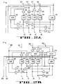
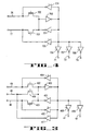
- FIG. 1 shows an overview of the general purpose register file of an 32 bit microcontroller according to the present invention. Only one plane showing one single bit of each register is shown in this drawing.
- the general purpose register file 1 comprises an address register file 2 and a data register file 3 that contain a plurality of address and data registers 4, 7 with a predetermined bit width and buffers 5, 6, 8, 9.
- the register bit width is 32 bits, and the number of registers is 16. This bit width can be any bit size according to the specification of the respective microcontroller, microprocessor or data handling unit.
- the address registers 4 are connected via a bus 13 to an address forward unit 5 and on the other hand to address load and store buffer 6.
- the data register file 1 contains a plurality of data registers 7, for example, 16 data registers with a bit width of 32 bit.
- a second bus 14 is provided which connects the data registers 7 on the one hand to data load and store buffers 9 and on the other hand to data forward unit 8.
- the general purpose register file 1 is on the one hand connected to a data memory unit 10 through a third bus 15 and on the other hand to additional buses 16, 17.
- Bus 16 connects the address forward buffers 5 and parts of the data forward buffers 8 to an unit 12 comprising, for example, an address arithmetic unit and an instruction fetch unit (IFU).
- Bus 17 connects the data forward buffers 8 to an unit 11 comprising, for example, a multiply accumulator (MAC) and an integer execution unit.
- MAC multiply accumulator
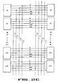
- FIGS 2A through 2F show the elements of the general purpose register file 1 in more detail. Only one bit of each register d0...d15, a0...a15 is shown in this diagram. The other 31 bits of the register d0...d15, a0...a15 are arranged in parallel. Throughout the Figures 2A to 2F the same numerals represent the same elements.
- Figure 2D shows registers in an address register file. For a better overview, registers a2 to a13 are not shown in Figure 2D. Every address register a0,... a15 of the address register file 4 has two uni-directional outputs for reading and three bidirectional I/O-ports.
- One internal bus line 40 is connected to the first bidirectional I/O-port of all address registers a0, ... a15, and two lines 41 and 42 are connected to the respective two outputs of all address registers a0,... a15.
- two internal bus lines 44 and 46 are connected to respective I/O-ports of all even address registers a0, a2, a4 ... a14.
- Two more lines 43 and 45 which are connected to the I/O-ports of all odd address registers a1, a3, a5...a15.
- FIG. 2A shows the address load and store buffer 6 of Figure 1 in detail.
- Bus lines 43 to 46 connect to the respective inputs of store buffers 101 to 104.
- the outputs of store buffers 101 to 104 are connected to memory bus lines 119 to 122 through drivers 106 to 109. All drivers are tri-state drivers which are provided with a control input for selective activation by means of a control unit (not shown).
- Two blocks 100 and 105 indicate 4 load buffers which are connected on the one hand to the memory bus lines 119 to 122 and on the other hand through drivers 110 to 113 to the internal bus lines 43 to 46.
- the outputs of the load buffer 105 are connected through buffers 115 and 116 to the internal bus lines 43 and 44.
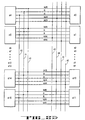
- FIG. 2E shows the address forward unit 5 of Figure 1 in detail.
- Bus lines 40, 41 and 42 are connected to address forward output bus lines 524, 525 and 526 through drivers 500, 501 and 502, respectively.
- Two memory bus lines 121 and 122 are each connected to the input of three drivers 503, 504, 505 and 506, 507, 508.
- the outputs of drivers 503 and 506 connect to bus line 526, the outputs of drivers 504 and 507 to bus line 525 and the outputs of drivers 505 and 508 to bus line 524.
- Internal bus lines 43 and 44 are connected to the outputs of two drivers 518 and 519, respectively.
- driver 518 and 519 are connected to the output of a write-back buffer 515 the input of which is connected to an address forward bus input line 523.
- Two other drivers 516 and 517 are provided the output of which are coupled with the internal bus line 40.
- the input of driver 517 is connected to the output of buffer 515.
- the input of driver 516 is connected to the output of buffer 514 the input of which is connected to address forward bus input line 522.
- Bus lines 45 and 46 are also connected to bus lines 522 and 523 through bidirectional drivers 520 and 521, respectively.
- the signal on bus line 523 is also fed to the inputs of three drivers 509, 510 and 511 the outputs of which are connected to bus lines 524, 525 and 526, respectively.
- the signal on bus line 522 is also fed to the inputs of two drivers 512 and 513 the outputs of which are connected to bus lines 524 and 525, respectively. Again, all drivers are tri-state drivers which are provided with a control input for selecting by means of a control unit (not shown).
- the three units 4, 5 and 6, according to Figure 1, show the path of the address signals into and out of the address register file, whereby bus lines 119 to 122, according to Figure 2A, connect to the memory unit 10 and bus lines 522 to 524 to the address arithmetic pipe and the instruction forward unit 12.
- Figure 2C shows data registers in a data register file. Again, for a better overview, registers d2 to d13 are not shown in Figure 2C. Every data register d0,... d15 of the data register file 5 has three uni-directional outputs for reading and two bidirectional I/O-ports. Two lines 72 and 73 are connected to the first two outputs of all data registers d0,... d15, respectively. Further, an internal bus lines 71 is connected to respective outputs of all even data registers d0, d2, d4 ... d14, whereas an internal bus line 70 is connected to respective outputs of all odd registers d1, d3, ... d15.
- Figure 2B shows the data load and store buffer 9 of Figure 1.
- Internal bus lines 74 to 77 are coupled to the inputs of four store buffers 909 to 912, respectively.
- the output of store buffer 909 is coupled to a memory bus line 921 through a driver 916, and the output of store buffer 910 is coupled to a memory bus line 920 through driver 917.
- the outputs of buffers 911 and 912 are connected to two input terminals of a mask unit 915.
- Mask unit 915 is provided with two input and two output terminals.
- the two output terminals of the mask unit 915 are coupled to two memory bus lines 922 and 923 through drivers 918 and 919, respectively.
- Two blocks 908 and 913 depict four load buffers.
- Block 913 is provided with two input terminals which are connected to two internal bus lines 900 and 901, respectively and to the memory bus lines 922 and 923 through an align block 914.
- the align block 914 is provided with two inputs which are connected to the inputs of mask unit 915 and the outputs of the store buffer 913, respectively.
- one output of load buffer 913 is coupled to internal bus lines 74 and 76 through respective drivers 904 and 906.
- the other output of load buffer 913 is coupled to internal bus lines 75 and 77 through drivers 905 and 907.
- the second load buffer 908 is connected on its input side to memory bus lines 920 and 921, respectively and on its output side to internal bus lines 74 and 75 through drivers 902 and 903, respectively.
- all drivers are tri-state drivers which are provided with a control input for selecting by means of a control unit (not shown).
- Figure 2F shows data forward unit 8 of Figure 1 in detail.
- Internal bus lines 70 to 73 are coupled with the data forward bus lines 802 to 805 through drivers 807 to 810.
- An additional data forward bus line 806 is connected to output terminals of drivers 827 and 828 the input terminals of which are connected to bus lines 802 and 803, respectively.
- Bus line 806 is part of the bus 16, according to Figure 1, which is connected to the address arithmetic pipe and instruction forward unit 12.
- Bus line 900 is connected to the inputs of three drivers 811, 812 and 813 the outputs of which are connected to bus lines 805, 804 and 802, respectively.
- Bus line 901 is connected to the inputs of three drivers 814, 815 and 816 the outputs of which are connected to bus lines 805, 804 and 803, respectively.
- Two other data forward bus lines 800 and 801 are provided which are coupled to the input terminals of two write-back buffers 829 and 830, respectively.
- the output terminals of buffers 829 and 830 are coupled to bus lines 74 and 75 through drivers 832 and 834, respectively.
- the output of buffer 830 is coupled to bus line 74 through a driver 833.
- Bus line 800 is coupled to bus line 76 through driver 835
- bus line 801 is also coupled to bus lines 76 and 77 through drivers 836 and 837, respectively.
- bus line 806 is coupled to bus lines 76 and 77 through drivers 840 and 841, respectively.
- bus line 806 is connected to the input terminal of a further write-back buffer 831 the output of which is coupled to bus lines 76 and 77 through drivers 838 and 839, respectively. Also, bus line 806 is coupled to bus lines 802 to 805 through drivers 817 to 820, respectively. Finally, bus line 800 is coupled to bus lines 805, 804 and 802 through drivers 821 to 823, respectively and bus line 801 is coupled to bus lines 803 to 805 through drivers 824 to 826, respectively. Again, all drivers are tri-state drivers which are provided with a control input for selecting by means of a control unit (not shown).
- the memory bus lines 119 to 122, according to Figure 2A, and 920 to 923, according to Figure 2B, form the memory bus 15 of Figure 1.
- the bus lines 522 to 526, according to Figure 2E, and 806 form bus 16 and bus lines 800 to 805 form bus 17 of Figure 1.
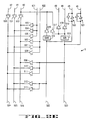
- Figure 3 shows an embodiment of an address register cell.
- Figure 3 shows numerals which are related to address register a0 according to Figure 2D.
- Preferably all registers a0 .. A15 have the same structure.
- the register core is formed by two inverters 400 and 401. These inverters 400 and 401 build a static memory cell, so that the output of each inverter is connected to the input of the other inverter. Input of inverter 400 and output of inverter 401 are coupled to bus lines 40, 44 and 46 through the load path of field effect transistors 402, 403 and 406. Each of field effect transistors 402, 403 and 406 forms a transfer-gate.
- inverter 400 and the input of inverter 401 is connected to the inputs of five controllable tri-state drivers 404, 405, 407, 408 and 409.
- the output of driver 404 is connected to bus line 40, the output of driver 405 to bus line 44 and the output of driver 407 to bus line 46.
- the output of driver 408 connects to bus line 41 and the output of driver 409 to bus line 42.
- Figure 4 shows an embodiment of a data register cell. Again, Figure 4 shows numerals which are related to data register d0 according to Figure 2C. Preferably, all registers d0 .. d15 have the same structure.
- the register core is formed by two inverters 700 and 701. These inverters 700 and 701 build a static memory cell, so that the output of each inverter is connected to the input of the other inverter. Input of inverter 700 and output of inverter 701 are coupled to bus lines 75 and 77 through the load path of field effect transistors 702 and 703.
- the output of inverter 700 and the input of inverter 701 are connected to the inputs of five controllable tri-state drivers 704, 705, 706, 707 and 708.
- the output of driver 704 is connected to bus line 75 and the output of driver 705 to bus line 77.
- the output of driver 706 connects to bus line 71, the output of driver 707 to bus line 72 and the output of driver 708 to bus line
- All other registers a1 ... a15 and d1 ... d15 are coupled to the respective bus lines as shown in Figures 2C and 2D.
- the transfer-gates 402, 403, 406, 702 and 703 (see Figures 3 and 4) and the tri-state drivers 404, 407, 408, 409, 704, 705, 706, 707 and 708 are controllable through respective select input terminals.
- the control circuit (not shown) generates the respective control signals to control the operation of these elements along with the other controllable drivers in the general purpose register file 1 (see Figure 1). Only one of the transfer-gates of a register can be activated at a time for write operations whereas a plurality of tri-state drivers can be active in parallel for any read operation.
- the general purpose registers handle all data which are processed by a data handling unit, such as a microcontroller/microcomputer. Therefore, they are part of the microprocessor/microcontroller core, and the way they handle the data has an important influence on the resulting speed of such a data handling unit.
- the general purpose register file 1 (see Figure 1) supplies most frequently used operands to the integer and load and store pipelines in the units 11, 12.
- the load and store instructions in the instruction set architecture provide access to the data memory 10 where a majority of operands reside before being brought into the register file 1.
- the functional block diagram for the register file is divided into address register file 2 and data register file 3. The data flow through the register files depends on the respective instruction which is being processed by the data handling unit.
- data and address register block 4 and 7 are arranged in two separate blocks.
- Data registers in block 7 are arranged in a first matrix having c1 columns and r1 rows and address registers in block 4 are arranged in a second matrix having c2 columns and r2 rows.
- both matrixes are equal whereby 2 columns and 8 rows are provided.
- 4 data registers in block 4 and 4 address registers in block 7 are arranged in parallel, so that 8 registers, 4 even and 4 odd registers, can be accessed through bidirectional ports on the memory interface side at the same time. Therefore, in this example, the bus 15, which interfaces on the one hand with the data memory unit and on the other hand with the below described data processing units, needs a width of 256 bits.
- the address register file 4 interfaces with any processing unit via bus 16.
- Bus 16 in this embodiment provides 6 bus lines, whereby 5 bus lines 522 .. 526 (see Figure 2E) connect to the address register file.
- the data register file 7 interfaces with any processing unit via bus 17.
- Bus 17, in this embodiment, provides 6 bus lines. Every register cell, in this embodiment, according to Figures 3 and 4, has 5 ports whereby two bidirectional ports are assigned to either even or odd registers. Therefore, in this embodiment, 7 data registers and 5 address registers can be accessed at the same time and provide data to any processing unit whereby some registers can only be accessed through the read port.
- m and n are integer numbers greater than 1 such that a minimum of 4 registers are accessible at the same time. Splitting the assignment of some ports into even and odd register sets can double this number.
- a context switch in a real time operating system may need 8 data registers and 8 address registers to be switched. In the preferred embodiment, this could be done in only 2 cycles, because 8 registers are accessible at the same time. If only 4 registers need to be changed for a context switch, this may be accomplished in a single cycle.
- each register is provided with a plurality of uni-directional and a plurality of bidirectional ports. This allows more registers to be accessed at the same time and also a wide variety of different instructions to be executed in a minimum of time. This occurs in parallel as described below.
- These uni-directional and bidirectional ports can be coupled one to one to the bus which is connected to the data memory. This allows access to as many registers as ports are provided at the same time, or the registers are split into even and odd register sets which are coupled to even and odd bus lines.
- the memory bus lines 119 and 121 as well as the memory bus lines 920 and 922 are coupled to odd registers in the address and data register file.
- Bus lines 120 and 122 as well as 921 and 923 are coupled to even registers, respectively. Therefore, only two ports of each register are used to interface with 4 registers of each register file 4 and 7 at the same time.
- the internal bus can comprise additional bus lines which connect to unidirectional and bidirectional ports of the registers. In this embodiment, these bus lines are 802 ... 806 and 524... 526 (see Figures 2F and 2E). Splitting between even and odd registers is optional for these bus lines. Even more registers can be accessed at the same time on the processing unit side, as described above.
- the bidirectional 256-bit bus interface on the data memory side of register file 1 supports the transfer of operands between data memory 10 and register file 1.
- This bus 15 could also be 128 bit wide or use 128-bits of 256-bit bus per cycle depending on the above described structure of the registers. The design of this bus can depend on power and noise related problems. Essentially, this bus has to support parallel access to at least 4 registers.
- the design according to the invention allows byte, half word, word and double-word transfers in a single cycle.
- the context save or restore operation allows for the transfer of 16 words in two cycles as mentioned above (four cycles on a 128-bit bus).
- the register file 1 is capable of saving or restoring the entire context (32 words) in 4 cycles (or eight cycles on 128-bit bus).
- the register file 1 supports word, double-word and quadruple-double word accesses.
- the data steering for byte, half-word and unaligned accesses is handled in the address load and store buffers 6, the data load and store buffers 9 and/or in the DMU module 10.
- the general purpose register file 1 of this embodiment contains thirty two 32-bit registers which, according to the principle of the present invention, are equally split to facilitate parallel operation of integer, and load and store instructions as described above.
- the DGPR 7 contains sixteen 32-bit data registers.
- the address portion of registers which supply address operands to the load and store pipeline reside in the address register file block 4 (AGPR).
- AGPR 4 contains sixteen 32-bit address registers.
- the instruction normally provides the register addresses for read and write accesses.
- the read and write address pointers are derived from the instruction in the instruction fetch stage and staged into the decode stage.
- the address in the read pointers is decoded to read the register operands in the decode stage.
- the address in write pointers is staged to the write-back stage.
- the decision for operand forwarding is made in the decode stage to minimize critical paths in the instruction fetch stage.
- Context instructions access a group of registers at a time in each register file 2, 3. For example, during context transfer, address registers a0, a1, a4, and a5 are accessed together during the first cycle, and address registers a2, a3, a6 and a7 are accessed together during the next cycle.
- the MAC instruction dictates the number of read and write ports in the data register file 7 which interface with the integer pipeline in unit 11.
- the context access dictates the requirement of number of bidirectional I/O-Ports in the data register file 7 which interface with the DMU 10.
- the structure of a single register has been explained in accordance with Figures 3 and 4. Due to the need for execution of integer and load and store instructions in parallel, ports are dedicated in the data register file 7 to interface exclusively with the integer pipeline of unit 11 and DMU 10.
- the read and write ports in DGPR 7 allow parallel operation of multiply- and load-instructions or of multiply- and store-instructions.
- the multiply-instruction in this embodiment requires four 32-bit read ports represented by bus lines 802 to 805 (see Figure 2F) and two 32-bit write ports represented by bus lines 800 and 801.
- the context access needs four 32-bit bidirectional ports represented by bus lines 920 to 923 (see Figure 2B) and internal buses 900 and 901 which are separate from the read ports dedicated for integer pipeline in unit 11.
- the load- and store-instructions could share two out of four context ports and internal buses 74 to 77 (see Figure 2B) which could be referred to as load and store ports and buses.
- the remaining two internal context buses could be shared by the integer pipeline for write-back operation which could be referred to as write-back buses.
- the context access dictates the number of bidirectional I/O-ports in the address register file 4 which interface with the DMU 10.
- the context access needs four 32-bit bidirectional ports represented by bus lines 119 to 122 (see Figure 2A) and internal buses which are separate from the read ports dedicated to the address arithmetic pipeline.
- bus lines 119 to 122 see Figure 2A
- internal buses which are separate from the read ports dedicated to the address arithmetic pipeline.
- one read/write port for each register which can be accessed in parallel must be provided. The number of ports therefore depends on the wide of the bus, or on the number of words which can be transferred in parallel on this bus.
- load- and store-instructions could share two out of four context ports and two out of four internal buses which could be referred to as load and store ports and buses.
- the remaining two internal context buses could be shared by the address arithmetic pipeline for write-back operation which could be referred to as write-back buses.
- a dedicated 32-bit bidirectional port represented by bus lines 800 handles transfers between the instruction fetch unit and the special function registers of unit 12 and address register file 4.
- Context and stack pointers share the write back bus to interface with general purpose file 1.
- a dedicated 32-bit bidirectional port 806 in the register file solves the data transfer problem between data and address register files.
- the data operand from a read port in the data register file 7 is steered to a read port in the address register file 4 through the bidirectional port.
- the result from the address arithmetic pipeline is steered to the load and store buses in the data register file 7 through the write port in the address register file 4 and the bidirectional port for write-back operation.
- a read-modify-write operation is performed to access the link word from the data memory during context save or restore operation.
- the context save operation uses a pointer to access the link word.
- the link word is loaded into the pointer register
- the contents from the pointer register are stored into a link word address location (as pointed to by the old pointer contents)
- the pointer register assumes the old pointer contents.
- the context restore operation uses the pointer register to access the link word.
- (a) the link word is loaded into the pointer register
- the contents from the pointer register are stored into a link word address location (as pointed to by the old pointer register contents)
- the pointer register assumes the old pointer contents.
- the register file 1 interfaces with the DMU 10 on one side, and on the other side directly connects to the address arithmetic pipeline IFU 12 and to MAC and integer pipelines 11.
- the controls for accessing the register file are derived from the instructions. To provide a better overview, these lines are not shown in Figures 2A to 2F.
- Address registers 4 are read in the first phase of the decode (or execute for store operand) cycle and written in the first phase of the write-back cycle to avoid having to forward a write-back result. For example, when the next+1 instruction needs the result from the current instruction (next being in the middle), the operand will be read directly from the address registers 4.
- Data registers 7 are read in the second phase of the decode (or execute for store operands) cycle and written in the second phase of the write-back cycle. Accessing address and data registers in alternate phases reduces peak power.
- the data register file 3 consists of the following blocks: data general purpose registers 7, load and store buffers 9 for data and, data forwarding buffers 8.
- the address register file 2 consists of the following blocks: address general purpose registers 4, load and store buffers 6 for address and, address forwarding unit 5.
- the data register file block 3 contains 16 data registers d0, .. d15.
- the basic data register cell in the data register file 7 has three read ports 71, 72, 73 (see Figure 2F) and two bidirectional ports 75 and 77. Two read ports 72 and 73 connect to all sixteen registers d0, ... d15 which enable access to any of these registers d0, ... d15.
- the read ports 70, 71 are connected either to even or odd registers, so that even registers d0, d2,... d14 are accessed through even port 71 and odd registers d1, d3, ... d15 are accessed through odd port 70.
- the MAC and other instructions need a third read operand.
- the MAC instruction requires a 64-bit accumulate operand which needs no further steering because it is already aligned to the even address boundary.
- the third operand is a 32-bit data as in some special instructions, depending on the register address, the operand could show up on the even or odd read port 71, 70 which needs further steering in the integer pipeline.
- the operand steering for the special instruction could be handled in the integer pipeline in its own input multiplexers which avoids the need of sending the controls to the register file 1. This eliminates one more read port in the data register file cell.
- Each bidirectional port 75, 77, 74, 76 in the register cell is connected either to even or odd registers, so that even registers d0, d2, ... d14 are accessed through even port 75, 77 and odd registers d1, d3, ... d15 are accessed through odd port 74, 76.
- the data result needs to be aligned or steered to appropriate buses from outside either in data memory unit 10 for load and store instructions or in data forward unit 8 for integer instructions.
- the data load and store buses 76 and 77 and the data write back buses 74 and 75 inside the data register file 3 are occupied respectively by integer and store instructions.
- the load data and destination register pointer stay in the load buffers until any of the buses 74 to 77 is made available. Meanwhile, the load buffers supply the data whenever the read pointer and destination pointer in the load buffers match.
- the load data occupies the data load and store bus lines 76, 77 while the write back result of integer instruction occupies the data write back bus lines 74, 75.
- the load data instead of using data load and store bus lines 76, 77, occupies the data write back bus lines 74, 75 while the store data occupies the data load and store bus lines 76, 77.
- the address register file block 2 contains 16 address registers.
- the basic register cell in the register has two read ports 41, 42 (see Figure 2E) and three bidirectional ports 40, 43, 44 or 40, 45, 46. However, both read ports 41, 42 and one bidirectional port 40 connect to all sixteen registers a0, ... a15.
- Address arithmetic instructions need only two read ports and one write port because they share the write-back buses.
- the load and store instructions use the load and store ports.
- the third bidirectional port is dedicated to loop- and jump-instructions. As usual, the address result needs to be aligned or steered outside either in data memory unit 10 for load and store instructions or in the address forward unit 5 for address arithmetic instructions to be able to access even and odd bidirectional ports.
- Data forward unit 8 forwards the load or integer results in the execute stage of the current instruction to the read ports in the decode stage of next instruction to minimize data dependent latency.
- Address forward unit 5 forwards the load or address arithmetic results in the execute stage of current instruction to the read ports in the decode stage of next instruction to minimize address dependent latency.
- the register contents are still read in the decode stage for next instruction even if the current instruction holds most recent data.
- the contents from the register are discarded if the current instruction has a most recent data result. If forward detection can be made for next instruction in the instruction fetch stage, register reading could be avoided for those operands whose address or data needs to be obtained from the results of current instruction in the execute stage hence saving power in the register file 1.
- a 32-bit bidirectional bus provides data transfers between data forwarding unit 8 and address forwarding unit 5.
- a special forwarding path allows execution of an integer followed by store instructions in parallel. The result from the integer pipeline in the execute stage is directly forwarded to the store buffers.
- the write back operation for integer instructions goes through write-back buffers 829, 830, 831 (see Figure 2F) in data forwarding unit 8.
- the write back operation for address arithmetic, loop- and some jump- instructions go through write-back buffer 515 (see Figure 2E) in address forwarding unit 5.
- the load and store buffer blocks 6 and 9 are functionally identical, except for the mask block 915 (see Figure 2B) in data load and store buffer 9.
- Data load and store buffer 9 and address load and store buffer 6 interface with the DMU 10 for context, load and store operations.
- the data load and store buffer 9 provides an interface between data register file 7 and the DMU 10.
- the address load and store buffer 6 provides an interface between address register file 2 and the DMU 10.
- Simple load and context load instructions use the load buffers 100, 105 (see Figure 2A), 908 and 913 (LDB) for write back operation. These load buffers 100, 105, 908 and 913 are separate from the write-back buffers in both data forward unit 5 and address forward unit 8.
- Context load instruction uses all four load buffers 100, 105, 908 and 913 for staging two double words during context write back operation. The different load instructions for double words use two load buffers for staging a double word during write back operation. The other load instructions and similar instructions use an even or odd load buffer of buffers 100, 105, 908 and 913 for staging a word for write back operation.
- the ALIGN sub-block 914 in data load and store buffer 9 handles zero and sign extension for byte and half-word load instructions.
- DMU 10 handles unpacking load data and data steering for unaligned, byte, half-word, word and double-word load operations in the load and store switch.
- Simple store and context store instructions use the store buffers (STB) 101 ... 104; 909 ... 912 for store operation.
- Context store instruction uses all four store buffers 101 ... 104; 909 ... 912 for staging two double words during context store operation.
- the double word store instructions use two store buffers for staging a double word during store operation.
- the other store instructions and similar instructions use even or odd store buffer 102, 104, 910, 912; 101, 103, 909, 911 for staging a word for store operation.
- DMU 10 handles packing store data and data steering for unaligned, byte, half-word, word and double-word store operations in the load and store switch.
- the swap instruction for words requires register that contents be swapped with data memory contents which could be viewed as a single cycle read-modify-write operation.
- the load and store buffers 6 and 9 handle the swap operation.
- the swap instruction for words performs a load instruction for words and a store instruction for words in parallel.
- the load data from data memory gets into the load buffers 908 and 913 and store data from register file gets into the store buffers 909 .. 912 in execute stage.
- the store data goes out to the data memory 10 and the load data gets into the data register file 7 in the write back stage.
- the peripheral interface (not shown) and internal memory treat swap instructions as two separate operations.
- the load and mask instruction uses mask unit 915 to perform a mask operation.
- the load operation reads the data memory and updates the load buffers 908 and 913 but does not update registers d0 ... d15.
- the store operation reads a double word from the registers d0 ... d15 and stores only a single word into the data memory 10.
- the data from data memory 10 gets into the load buffers 908 and 913 and store data from register file 7 gets into the store buffers in the execute stage.
- the mask unit 915 uses upper word from the store buffers 911 and 912 to merge the lower word with the output from the load buffers 908 and 913.
- the store data goes out to the data memory 10 in the write back stage.
- a cache memory can be optionally provided to improve access to the data stored in the memory.
Landscapes
- Engineering & Computer Science (AREA)
- Software Systems (AREA)
- Theoretical Computer Science (AREA)
- Physics & Mathematics (AREA)
- General Engineering & Computer Science (AREA)
- General Physics & Mathematics (AREA)
- Executing Machine-Instructions (AREA)
- Memory System Of A Hierarchy Structure (AREA)
Description
- The present invention relates to a processing unit and, in particular, to a central processing unit (CPU) such as a microcontroller. Microcontrollers are well known in the art, and a large variety of such devices from low end devices (e.g., a 4/8-bit controller) to high end devices (e.g., a 32-bit controller) are available. High end controllers are used in almost any kind of electronic devices, such as laser printers and hard disks or for controlling any kind of processes, for example, in automobiles, etc.
- With more complex tasks to be solved, the demand for very fast, high end controllers is rising. In particular, such devices are necessary to control real time applications. In such applications, it is necessary to react very fast to external events. If such an event occurs, the content of at least a specific set of registers needs to be switched. If this context switching is faster, the reaction time of the control system is better.
-
EP-A-0 745 933 (IBM) 4 December 1996 (1996-12-04) discloses a multiple port register file for use with Very Long Instruction Word (VLIW) and N-way superscalar processors. Said register file includes a selected number of copies of a general purpose register building block. The block includes two interleaved sub-banks of registers (odd and even registers) each comprising a number n of write ports and a number m of read ports. The sub-banks are interleaved by write ports and have non-interleaved read ports. - Therefore, it is an object of the present invention to provide a processing unit with the capability of very fast read/write access to address and data registers in a CPU.
- This object is achieved by means of a data processing unit as set out in
claim 1 having a set of data registers and a set of address registers. Each register has a width of n bits. Furthermore, there are provided address load and store buffers associated with said address registers, data load and store buffers associated with said data registers and a bus having a plurality of bus lines being connected to said store buffers. A data memory unit is connected to said bus. The data registers are arranged in such a way that at least n data registers are connected in parallel to respective bus lines, n being greater than 1 and the address registers are arranged in such a way, that at least m address registers are coupled in parallel to respective bus lines, m being greater than 1. Thus, at least four registers can be accessed in parallel. - If, for example, 4 data registers and 4 address registers can be loaded or stored simultaneously, then a 32-bit microcontroller-bus has to be 256 bits wide. The advantage of such an arrangement is, that a context switch can be done very fast because 8 registers are stored and loaded in only 2 respective cycles. This allows a very fast reaction time to external events. Also, processing time is speed up because commands can be implemented that provide parallel processing. That is, more than one register can be loaded or stored at the same time.
- To enable multi-register read and write procedures, each register is provided with multiple uni- and/or multiple bidirectional ports, which couple the registers with a memory unit and/or with an address arithmetic pipe or an integer pipe or any other processing unit. The registers can be divided into different sets of registers, for example, even and odd registers. Thus, an optimized layout of the respective registers is possible, while accessibility to the registers is maintained. Each of the above mentioned lines can be selected separately, and the lines are linked to odd or even memory addresses.
- A wide variety of implementations is possible. Either all register cells communicate through one multiple-word-wide bus, whereby each register cell has a plurality of read/write lines which are connected to each word lines of the multiple-word-wide bus, or different set of registers connect to respective word lines of the multiple-word-wide bus which connects to the memory. Multiplexers and alignment units can couple any register with any address location within the memory.
- Further, a unit is provided which handles zero and sign extension for byte and half-word load instructions. The address registers can be connected to an address arithmetic unit or any other processing unit through an address forward buffer, and the data registers can be coupled to a multiply accumulator unit (MAC) and/or Integer execution unit or any other processing unit through a respective data forward buffer.
-
- Figure 1 shows a functional block diagram of a register file according to the present invention,
- Figure 2A shows a data load and store buffer unit,
- Figure 2B shows an address load and store buffer unit,
- Figure 2C shows a data register file unit,
- Figure 2D shows an address register file unit,
- Figure 2E shows a data forward unit,
- Figure 2F shows an address forward unit,
- Figure 3 shows a address register cell in more detail, and
- Figure 4 shows a data register cell in more detail.
- Figure 1 shows an overview of the general purpose register file of an 32 bit microcontroller according to the present invention. Only one plane showing one single bit of each register is shown in this drawing. The general
purpose register file 1 comprises anaddress register file 2 and adata register file 3 that contain a plurality of address anddata registers 4, 7 with a predetermined bit width andbuffers - On the one hand, the address registers 4 are connected via a
bus 13 to an addressforward unit 5 and on the other hand to address load andstore buffer 6. Further, thedata register file 1 contains a plurality ofdata registers 7, for example, 16 data registers with a bit width of 32 bit. Asecond bus 14 is provided which connects thedata registers 7 on the one hand to data load andstore buffers 9 and on the other hand todata forward unit 8. The generalpurpose register file 1 is on the one hand connected to adata memory unit 10 through athird bus 15 and on the other hand toadditional buses Bus 16 connects the addressforward buffers 5 and parts of the dataforward buffers 8 to anunit 12 comprising, for example, an address arithmetic unit and an instruction fetch unit (IFU).Bus 17 connects the dataforward buffers 8 to anunit 11 comprising, for example, a multiply accumulator (MAC) and an integer execution unit. - Figures 2A through 2F show the elements of the general
purpose register file 1 in more detail. Only one bit of each register d0...d15, a0...a15 is shown in this diagram. The other 31 bits of the register d0...d15, a0...a15 are arranged in parallel. Throughout the Figures 2A to 2F the same numerals represent the same elements. - Figure 2D shows registers in an address register file. For a better overview, registers a2 to a13 are not shown in Figure 2D. Every address register a0,... a15 of the address register file 4 has two uni-directional outputs for reading and three bidirectional I/O-ports. One
internal bus line 40 is connected to the first bidirectional I/O-port of all address registers a0, ... a15, and twolines internal bus lines more lines - Figure 2A shows the address load and
store buffer 6 of Figure 1 in detail.Bus lines 43 to 46 connect to the respective inputs ofstore buffers 101 to 104. The outputs ofstore buffers 101 to 104 are connected tomemory bus lines 119 to 122 throughdrivers 106 to 109. All drivers are tri-state drivers which are provided with a control input for selective activation by means of a control unit (not shown). Twoblocks memory bus lines 119 to 122 and on the other hand throughdrivers 110 to 113 to theinternal bus lines 43 to 46. In addition, the outputs of theload buffer 105 are connected throughbuffers internal bus lines - Figure 2E shows the address
forward unit 5 of Figure 1 in detail.Bus lines output bus lines drivers memory bus lines drivers drivers bus line 526, the outputs ofdrivers bus line 525 and the outputs ofdrivers bus line 524.Internal bus lines drivers drivers back buffer 515 the input of which is connected to an address forwardbus input line 523. Twoother drivers internal bus line 40. The input ofdriver 517 is connected to the output ofbuffer 515. The input ofdriver 516 is connected to the output ofbuffer 514 the input of which is connected to address forwardbus input line 522.Bus lines bus lines bidirectional drivers bus line 523 is also fed to the inputs of threedrivers bus lines bus line 522 is also fed to the inputs of twodrivers bus lines units bus lines 119 to 122, according to Figure 2A, connect to thememory unit 10 andbus lines 522 to 524 to the address arithmetic pipe and theinstruction forward unit 12. - Figure 2C shows data registers in a data register file. Again, for a better overview, registers d2 to d13 are not shown in Figure 2C. Every data register d0,... d15 of the
data register file 5 has three uni-directional outputs for reading and two bidirectional I/O-ports. Twolines internal bus lines 71 is connected to respective outputs of all even data registers d0, d2, d4 ... d14, whereas aninternal bus line 70 is connected to respective outputs of all odd registers d1, d3, ... d15. Twomore lines other lines - Figure 2B shows the data load and
store buffer 9 of Figure 1.Internal bus lines 74 to 77 are coupled to the inputs of fourstore buffers 909 to 912, respectively. The output ofstore buffer 909 is coupled to amemory bus line 921 through adriver 916, and the output ofstore buffer 910 is coupled to amemory bus line 920 throughdriver 917. The outputs ofbuffers mask unit 915.Mask unit 915 is provided with two input and two output terminals. The two output terminals of themask unit 915 are coupled to twomemory bus lines drivers blocks Block 913 is provided with two input terminals which are connected to twointernal bus lines memory bus lines align block 914. Thealign block 914 is provided with two inputs which are connected to the inputs ofmask unit 915 and the outputs of thestore buffer 913, respectively. Furthermore, one output ofload buffer 913 is coupled tointernal bus lines respective drivers load buffer 913 is coupled tointernal bus lines drivers second load buffer 908 is connected on its input side tomemory bus lines internal bus lines drivers - Figure 2F shows data
forward unit 8 of Figure 1 in detail.Internal bus lines 70 to 73 are coupled with the dataforward bus lines 802 to 805 throughdrivers 807 to 810. An additional dataforward bus line 806 is connected to output terminals ofdrivers bus lines Bus line 806 is part of thebus 16, according to Figure 1, which is connected to the address arithmetic pipe and instruction forwardunit 12.Bus line 900 is connected to the inputs of threedrivers bus lines Bus line 901 is connected to the inputs of threedrivers bus lines forward bus lines back buffers buffers bus lines drivers 832 and 834, respectively. In addition, the output ofbuffer 830 is coupled tobus line 74 through adriver 833.Bus line 800 is coupled tobus line 76 throughdriver 835, andbus line 801 is also coupled tobus lines drivers 836 and 837, respectively. Also,bus line 806 is coupled tobus lines drivers bus line 806 is connected to the input terminal of a further write-back buffer 831 the output of which is coupled tobus lines drivers bus line 806 is coupled tobus lines 802 to 805 throughdrivers 817 to 820, respectively. Finally,bus line 800 is coupled tobus lines drivers 821 to 823, respectively andbus line 801 is coupled tobus lines 803 to 805 throughdrivers 824 to 826, respectively. Again, all drivers are tri-state drivers which are provided with a control input for selecting by means of a control unit (not shown). Thememory bus lines 119 to 122, according to Figure 2A, and 920 to 923, according to Figure 2B, form thememory bus 15 of Figure 1. Thebus lines 522 to 526, according to Figure 2E, and 806form bus 16 andbus lines 800 to 805form bus 17 of Figure 1. - Figure 3 shows an embodiment of an address register cell. Figure 3 shows numerals which are related to address register a0 according to Figure 2D. Preferably all registers a0 .. A15 have the same structure. The register core is formed by two
inverters inverters inverter 400 and output ofinverter 401 are coupled tobus lines field effect transistors field effect transistors inverter 400 and the input ofinverter 401 is connected to the inputs of five controllabletri-state drivers driver 404 is connected tobus line 40, the output ofdriver 405 tobus line 44 and the output ofdriver 407 tobus line 46. The output ofdriver 408 connects tobus line 41 and the output ofdriver 409 tobus line 42. - Figure 4 shows an embodiment of a data register cell. Again, Figure 4 shows numerals which are related to data register d0 according to Figure 2C. Preferably, all registers d0 .. d15 have the same structure. The register core is formed by two
inverters inverters inverter 700 and output ofinverter 701 are coupled tobus lines field effect transistors inverter 700 and the input ofinverter 701 are connected to the inputs of five controllabletri-state drivers driver 704 is connected tobus line 75 and the output ofdriver 705 tobus line 77. The output ofdriver 706 connects tobus line 71, the output ofdriver 707 tobus line 72 and the output ofdriver 708 tobus line 73. - All other registers a1 ... a15 and d1 ... d15 are coupled to the respective bus lines as shown in Figures 2C and 2D. The transfer-
gates tri-state drivers - The general purpose registers handle all data which are processed by a data handling unit, such as a microcontroller/microcomputer. Therefore, they are part of the microprocessor/microcontroller core, and the way they handle the data has an important influence on the resulting speed of such a data handling unit. The general purpose register file 1 (see Figure 1) supplies most frequently used operands to the integer and load and store pipelines in the
units data memory 10 where a majority of operands reside before being brought into theregister file 1. As shown in Figure 1, the functional block diagram for the register file is divided intoaddress register file 2 and data registerfile 3. The data flow through the register files depends on the respective instruction which is being processed by the data handling unit. - According to the invention, data and
address register block 4 and 7 are arranged in two separate blocks. Data registers inblock 7 are arranged in a first matrix having c1 columns and r1 rows and address registers in block 4 are arranged in a second matrix having c2 columns and r2 rows. In the preferred embodiment, both matrixes are equal whereby 2 columns and 8 rows are provided. Nevertheless, in this embodiment, 4 data registers in block 4 and 4 address registers inblock 7 are arranged in parallel, so that 8 registers, 4 even and 4 odd registers, can be accessed through bidirectional ports on the memory interface side at the same time. Therefore, in this example, thebus 15, which interfaces on the one hand with the data memory unit and on the other hand with the below described data processing units, needs a width of 256 bits. - On the processing unit side, the address register file 4 interfaces with any processing unit via
bus 16.Bus 16, in this embodiment provides 6 bus lines, whereby 5bus lines 522 .. 526 (see Figure 2E) connect to the address register file. The data registerfile 7 interfaces with any processing unit viabus 17.Bus 17, in this embodiment, provides 6 bus lines. Every register cell, in this embodiment, according to Figures 3 and 4, has 5 ports whereby two bidirectional ports are assigned to either even or odd registers. Therefore, in this embodiment, 7 data registers and 5 address registers can be accessed at the same time and provide data to any processing unit whereby some registers can only be accessed through the read port. - Depending on the operating system running the microcontroller, this arrangement results in access to a plurality of general purpose registers of the core in one single cycle. According to the invention, m and n are integer numbers greater than 1 such that a minimum of 4 registers are accessible at the same time. Splitting the assignment of some ports into even and odd register sets can double this number. A context switch in a real time operating system may need 8 data registers and 8 address registers to be switched. In the preferred embodiment, this could be done in only 2 cycles, because 8 registers are accessible at the same time. If only 4 registers need to be changed for a context switch, this may be accomplished in a single cycle.
- According to the invention, each register is provided with a plurality of uni-directional and a plurality of bidirectional ports. This allows more registers to be accessed at the same time and also a wide variety of different instructions to be executed in a minimum of time. This occurs in parallel as described below. These uni-directional and bidirectional ports can be coupled one to one to the bus which is connected to the data memory. This allows access to as many registers as ports are provided at the same time, or the registers are split into even and odd register sets which are coupled to even and odd bus lines. In the embodiment according to Figures 2A and 2B, the
memory bus lines memory bus lines Bus lines register file 4 and 7 at the same time. On the data processing side, the internal bus can comprise additional bus lines which connect to unidirectional and bidirectional ports of the registers. In this embodiment, these bus lines are 802 ... 806 and 524... 526 (see Figures 2F and 2E). Splitting between even and odd registers is optional for these bus lines. Even more registers can be accessed at the same time on the processing unit side, as described above. - The bidirectional 256-bit bus interface on the data memory side of
register file 1 supports the transfer of operands betweendata memory 10 and registerfile 1. Thisbus 15 could also be 128 bit wide or use 128-bits of 256-bit bus per cycle depending on the above described structure of the registers. The design of this bus can depend on power and noise related problems. Essentially, this bus has to support parallel access to at least 4 registers. - The design according to the invention allows byte, half word, word and double-word transfers in a single cycle. The context save or restore operation allows for the transfer of 16 words in two cycles as mentioned above (four cycles on a 128-bit bus). However, the
register file 1 is capable of saving or restoring the entire context (32 words) in 4 cycles (or eight cycles on 128-bit bus). In general, theregister file 1 supports word, double-word and quadruple-double word accesses. The data steering for byte, half-word and unaligned accesses is handled in the address load andstore buffers 6, the data load andstore buffers 9 and/or in theDMU module 10. - The general
purpose register file 1 of this embodiment contains thirty two 32-bit registers which, according to the principle of the present invention, are equally split to facilitate parallel operation of integer, and load and store instructions as described above. The data portion of registers, which supply data operands to the integer pipeline, reside in the data register file block 7 (DGPR). TheDGPR 7 contains sixteen 32-bit data registers. The address portion of registers which supply address operands to the load and store pipeline reside in the address register file block 4 (AGPR). The AGPR 4 contains sixteen 32-bit address registers. The instruction normally provides the register addresses for read and write accesses. The read and write address pointers are derived from the instruction in the instruction fetch stage and staged into the decode stage. The address in the read pointers is decoded to read the register operands in the decode stage. The address in write pointers is staged to the write-back stage. The decision for operand forwarding is made in the decode stage to minimize critical paths in the instruction fetch stage. - Context instructions, with implied address sequence, access a group of registers at a time in each
register file - In this embodiment, the MAC instruction dictates the number of read and write ports in the
data register file 7 which interface with the integer pipeline inunit 11. Also, the context access dictates the requirement of number of bidirectional I/O-Ports in thedata register file 7 which interface with theDMU 10. The structure of a single register has been explained in accordance with Figures 3 and 4. Due to the need for execution of integer and load and store instructions in parallel, ports are dedicated in thedata register file 7 to interface exclusively with the integer pipeline ofunit 11 andDMU 10. The read and write ports inDGPR 7 allow parallel operation of multiply- and load-instructions or of multiply- and store-instructions. The multiply-instruction in this embodiment, for example, requires four 32-bit read ports represented bybus lines 802 to 805 (see Figure 2F) and two 32-bit write ports represented bybus lines bus lines 920 to 923 (see Figure 2B) andinternal buses unit 11. The load- and store-instructions could share two out of four context ports andinternal buses 74 to 77 (see Figure 2B) which could be referred to as load and store ports and buses. The remaining two internal context buses could be shared by the integer pipeline for write-back operation which could be referred to as write-back buses. - Many address arithmetic instructions require two 32-bit read ports and one 32-bit write port in the address register file 4 to interface with the address arithmetic pipeline in
unit 12. In this embodiment, the context access dictates the number of bidirectional I/O-ports in the address register file 4 which interface with theDMU 10. In the preferred embodiment, the context access needs four 32-bit bidirectional ports represented bybus lines 119 to 122 (see Figure 2A) and internal buses which are separate from the read ports dedicated to the address arithmetic pipeline. In other words, one read/write port for each register which can be accessed in parallel must be provided. The number of ports therefore depends on the wide of the bus, or on the number of words which can be transferred in parallel on this bus. The load- and store-instructions could share two out of four context ports and two out of four internal buses which could be referred to as load and store ports and buses. The remaining two internal context buses could be shared by the address arithmetic pipeline for write-back operation which could be referred to as write-back buses. A dedicated 32-bit bidirectional port represented by bus lines 800 (see Figure 2F) handles transfers between the instruction fetch unit and the special function registers ofunit 12 and address register file 4. Context and stack pointers share the write back bus to interface withgeneral purpose file 1. - Due to the limitation on the number of read and write ports available in the
register file 1, instructions involving both data and address registers share existing ports only. As a result, in this embodiment, many address arithmetic operations when issued in parallel with integer instructions may need to be canceled in the current cycle and are-injected in the following cycle. A dedicated 32-bit bidirectional port 806 (see Figure 2F) in the register file solves the data transfer problem between data and address register files. The data operand from a read port in thedata register file 7 is steered to a read port in the address register file 4 through the bidirectional port. The result from the address arithmetic pipeline is steered to the load and store buses in thedata register file 7 through the write port in the address register file 4 and the bidirectional port for write-back operation. - A read-modify-write operation is performed to access the link word from the data memory during context save or restore operation. The context save operation uses a pointer to access the link word. During context save operation, (a) the link word is loaded into the pointer register, (b) the contents from the pointer register are stored into a link word address location (as pointed to by the old pointer contents), and (c) the pointer register assumes the old pointer contents. The context restore operation uses the pointer register to access the link word. During context restore operation, (a) the link word is loaded into the pointer register, (b) the contents from the pointer register are stored into a link word address location (as pointed to by the old pointer register contents), and (c) the pointer register assumes the old pointer contents.
- The
register file 1 interfaces with theDMU 10 on one side, and on the other side directly connects to the addressarithmetic pipeline IFU 12 and to MAC andinteger pipelines 11. The controls for accessing the register file are derived from the instructions. To provide a better overview, these lines are not shown in Figures 2A to 2F. Address registers 4 are read in the first phase of the decode (or execute for store operand) cycle and written in the first phase of the write-back cycle to avoid having to forward a write-back result. For example, when the next+1 instruction needs the result from the current instruction (next being in the middle), the operand will be read directly from the address registers 4. Data registers 7 are read in the second phase of the decode (or execute for store operands) cycle and written in the second phase of the write-back cycle. Accessing address and data registers in alternate phases reduces peak power. The data registerfile 3 consists of the following blocks: data general purpose registers 7, load andstore buffers 9 for data and,data forwarding buffers 8. Theaddress register file 2 consists of the following blocks: address general purpose registers 4, load andstore buffers 6 for address and, address forwardingunit 5. - In the preferred embodiment, the data
register file block 3 contains 16 data registers d0, .. d15. The basic data register cell in thedata register file 7 has three readports bidirectional ports ports ports port 71 and odd registers d1, d3, ... d15 are accessed throughodd port 70. The MAC and other instructions need a third read operand. The MAC instruction requires a 64-bit accumulate operand which needs no further steering because it is already aligned to the even address boundary. However, if the third operand is a 32-bit data as in some special instructions, depending on the register address, the operand could show up on the even orodd read port register file 1. This eliminates one more read port in the data register file cell. - Each
bidirectional port port odd port data memory unit 10 for load and store instructions or in dataforward unit 8 for integer instructions. - When integer, load and store instructions are issued in sequence, the data load and
store buses buses data register file 3 are occupied respectively by integer and store instructions. The load data and destination register pointer stay in the load buffers until any of thebuses 74 to 77 is made available. Meanwhile, the load buffers supply the data whenever the read pointer and destination pointer in the load buffers match. - For an integer followed by a load instruction sequence, the load data occupies the data load and
store bus lines bus lines store bus lines bus lines store bus lines - The address
register file block 2 contains 16 address registers. The basic register cell in the register has two readports 41, 42 (see Figure 2E) and threebidirectional ports ports bidirectional port 40 connect to all sixteen registers a0, ... a15. Address arithmetic instructions need only two read ports and one write port because they share the write-back buses. The load and store instructions use the load and store ports. The third bidirectional port is dedicated to loop- and jump-instructions. As usual, the address result needs to be aligned or steered outside either indata memory unit 10 for load and store instructions or in the addressforward unit 5 for address arithmetic instructions to be able to access even and odd bidirectional ports. - Data
forward unit 8 forwards the load or integer results in the execute stage of the current instruction to the read ports in the decode stage of next instruction to minimize data dependent latency. Addressforward unit 5 forwards the load or address arithmetic results in the execute stage of current instruction to the read ports in the decode stage of next instruction to minimize address dependent latency. The register contents are still read in the decode stage for next instruction even if the current instruction holds most recent data. The contents from the register are discarded if the current instruction has a most recent data result. If forward detection can be made for next instruction in the instruction fetch stage, register reading could be avoided for those operands whose address or data needs to be obtained from the results of current instruction in the execute stage hence saving power in theregister file 1. - The integer followed by a load and store or an address arithmetic instruction could be issued in parallel. However, in this embodiment, if the result of the integer instruction needs to be forwarded to the address arithmetic pipeline, the instruction in the address arithmetic pipeline stalls for one cycle. The result forwarding from the address arithmetic pipeline to the integer pipeline does not need to stall the integer pipeline because the address arithmetic, load or store followed by integer instructions are never issued in parallel. A 32-bit bidirectional bus provides data transfers between
data forwarding unit 8 and address forwardingunit 5. A special forwarding path allows execution of an integer followed by store instructions in parallel. The result from the integer pipeline in the execute stage is directly forwarded to the store buffers. - The write back operation for integer instructions goes through write-
back buffers data forwarding unit 8. The write back operation for address arithmetic, loop- and some jump- instructions go through write-back buffer 515 (see Figure 2E) inaddress forwarding unit 5. - The load and store buffer blocks 6 and 9 are functionally identical, except for the mask block 915 (see Figure 2B) in data load and
store buffer 9. Data load andstore buffer 9 and address load andstore buffer 6 interface with theDMU 10 for context, load and store operations. The data load andstore buffer 9 provides an interface between data registerfile 7 and theDMU 10. The address load andstore buffer 6 provides an interface betweenaddress register file 2 and theDMU 10. Even though the data path diagram of Figures 2A to 2F shows the configuration forbit 0, the same configuration applies to all bits in the diagram. - Simple load and context load instructions use the load buffers 100, 105 (see Figure 2A), 908 and 913 (LDB) for write back operation. These load buffers 100, 105, 908 and 913 are separate from the write-back buffers in both data
forward unit 5 and addressforward unit 8. Context load instruction uses all fourload buffers buffers - The ALIGN sub-block 914 in data load and
store buffer 9 handles zero and sign extension for byte and half-word load instructions. However,DMU 10 handles unpacking load data and data steering for unaligned, byte, half-word, word and double-word load operations in the load and store switch. - Simple store and context store instructions use the store buffers (STB) 101 ... 104; 909 ... 912 for store operation. Context store instruction uses all four
store buffers 101 ... 104; 909 ... 912 for staging two double words during context store operation. The double word store instructions use two store buffers for staging a double word during store operation. The other store instructions and similar instructions use even orodd store buffer DMU 10 handles packing store data and data steering for unaligned, byte, half-word, word and double-word store operations in the load and store switch. - The swap instruction for words requires register that contents be swapped with data memory contents which could be viewed as a single cycle read-modify-write operation. The load and
store buffers data memory 10 and the load data gets into thedata register file 7 in the write back stage. The peripheral interface (not shown) and internal memory treat swap instructions as two separate operations. - For a special load and mask instruction a single cycle read-modify-write operation is required, and this instruction performs operations similar to the above mentioned swap instruction with a few minor changes. The load and mask instruction uses
mask unit 915 to perform a mask operation. The load operation reads the data memory and updates the load buffers 908 and 913 but does not update registers d0 ... d15. The store operation reads a double word from the registers d0 ... d15 and stores only a single word into thedata memory 10. The data fromdata memory 10 gets into the load buffers 908 and 913 and store data fromregister file 7 gets into the store buffers in the execute stage. Themask unit 915 uses upper word from the store buffers 911 and 912 to merge the lower word with the output from the load buffers 908 and 913. The store data goes out to thedata memory 10 in the write back stage. Between thedata memory unit 10 and the general purpose register file, a cache memory can be optionally provided to improve access to the data stored in the memory.
Claims (14)
- A data processing unit (1) comprising
a set (3) of data registers (d0, d1, ..., d15) and a set of address registers (a0, a1, ..., a15), each register having a width of n bits, and each set of data and address registers comprising even and odd data and address registers, respectively,
first address load (100, 105) and store (102, 104) buffers associated with said even (a0, a1, ..., a14) address registers and second address load (100, 105) and store (101, 103) buffers associated with said odd (a1, a3, ..., a15) address registers,
first data load (908, 913) and store (910, 912) buffers associated with said even (d0, d2, ..., d14) data registers and second data load (908, 913) and store (909, 911) buffers associated with said odd (d1, d3, ..., d15) data registers,
a bus having a plurality of bus lines (43 - 46, 74 - 77) comprising a width of 4n bits being connected to said first and second load and store buffers (100, 105, 908, 913, 101 - 104, 909 - 912),
a data memory unit (10) being connected to said bus, wherein 2n-bit data words and 2n-bit address words can be transferred from or to said memory (10) to or from one of said even (d0, d2, ..., d14), one of said odd (d1, d3, ..., d15) data registers, one of said even (a0, a2, ..., a14), and one of said odd (a1, a3, ..., a15) address registers in parallel. - Data processing unit (1) as in claim 1, wherein each register has a plurality of ports and at least one of said bus lines (43 - 46, 74 - 77) is coupled in parallel to one of said ports of each register.
- Data processing unit (1) as in claim 2, wherein each register comprises a memory cell (400, 401, 700, 701) having an input terminal and an output terminal, a plurality of tri-state buffers (404, 405, 407, 408, 409, 704 - 708) with inputs and outputs, said output terminal being connected to the inputs of said plurality of tri-state buffers (404, 405, 407, 408, 409, 704 - 708).
- Data processing unit (1) as in claim 3, wherein each register further comprises a plurality of transfer gates (402, 403, 406, 702, 703), said input terminal of said memory cell (400, 401, 700, 701) being connected to the outputs of said plurality of transfer gates (402, 403, 406, 702, 703).
- Data processing unit (1) as in claim 1, further comprising an address forward unit (5) associated with said address registers (a0, a1, ..., a15) and a processing unit (12) connected to said address forward unit (5).
- Data processing unit as in claim 5, wherein each address register (a0, a1, ..., a15) has a plurality of ports, the address forward unit (5) has a plurality of terminals, at least one of said terminals is coupled to one of said ports of at least one of said address registers (a0, a1, ..., a15).
- Data processing unit (1) as in claim 6, wherein each register (a0, a1, ..., a15) comprises a memory cell (400, 401) having an input terminal and an output terminal, a plurality of tri-state buffers (404, 405, 407, 408, 409) with inputs and outputs, said output terminal being connected to the inputs of said plurality of tri-state buffers (404, 405, 407, 408, 409).
- Data processing unit (1) as in claim 7, wherein each register (a0, a1, ..., a15) further comprises a plurality of transfer gates (402, 403, 406), said input terminal of said memory cell (400, 401) being connected to the outputs of said plurality of transfer gates (402, 403, 406).
- Data processing unit (1) as in claim 1, further comprising a data forward buffer (8) associated with said data registers (d0, d1, ..., d15) and a processing unit (11) connected to said data forward buffer (B).
- Data processing unit (1) as in claim 9, wherein each data register (d0, d1, ..., d15) has a plurality of ports, the data forward unit has a plurality of terminals, at least one of said terminals is coupled to one of said ports of at least one of said data registers (d0, d1, ..., d15).
- Data processing unit (1) as in claim 10, wherein each register (d0, d1, ..., d15) comprises a memory cell (700, 701) having an input terminal and an output terminal, a plurality of tri-state buffers (704 - 708) with inputs and outputs, said output terminal being connected to the inputs of said plurality of tri-state buffers (704 - 708).
- Data processing unit (1) as in claim 11, wherein each register (d0, d1, ..., d15) further comprises a plurality of transfer gates (702, 703), said input terminal of said memory cell (700, 701) being connected to the outputs of said plurality of transfer gates (702, 703).
- Data processing unit (1) as in claim 1, wherein an align unit (914) is provided which connects even or odd registers to even or odd addresses of the memory through said bus.
- Data processing unit (1) as in claim 1, wherein a mask unit (915) is provided which is connected to at least one port of at least one of said registers.
Applications Claiming Priority (2)
| Application Number | Priority Date | Filing Date | Title |
|---|---|---|---|
| US08/928,428 US6041387A (en) | 1997-09-12 | 1997-09-12 | Apparatus for read/write-access to registers having register file architecture in a central processing unit |
| US928428 | 1997-09-12 |
Publications (3)
| Publication Number | Publication Date |
|---|---|
| EP0902360A2 EP0902360A2 (en) | 1999-03-17 |
| EP0902360A3 EP0902360A3 (en) | 2002-09-04 |
| EP0902360B1 true EP0902360B1 (en) | 2007-11-14 |
Family
ID=25456221
Family Applications (1)
| Application Number | Title | Priority Date | Filing Date |
|---|---|---|---|
| EP98117255A Expired - Lifetime EP0902360B1 (en) | 1997-09-12 | 1998-09-11 | Apparatus for read/write-access to registers in a central processing unit |
Country Status (5)
| Country | Link |
|---|---|
| US (1) | US6041387A (en) |
| EP (1) | EP0902360B1 (en) |
| JP (1) | JPH11154089A (en) |
| KR (1) | KR19990029748A (en) |
| DE (1) | DE69838701T2 (en) |
Families Citing this family (25)
| Publication number | Priority date | Publication date | Assignee | Title |
|---|---|---|---|---|
| US6567910B2 (en) * | 1998-02-13 | 2003-05-20 | Texas Instruments Incorporated | Digital signal processing unit with emulation circuitry and debug interrupt enable register indicating serviceable time-critical interrupts during real-time emulation mode |
| US6256725B1 (en) * | 1998-12-04 | 2001-07-03 | Agere Systems Guardian Corp. | Shared datapath processor utilizing stack-based and register-based storage spaces |
| EP1050800A1 (en) | 1999-05-03 | 2000-11-08 | STMicroelectronics SA | A pipelined execution unit |
| US6397324B1 (en) * | 1999-06-18 | 2002-05-28 | Bops, Inc. | Accessing tables in memory banks using load and store address generators sharing store read port of compute register file separated from address register file |
| US6732255B1 (en) * | 1999-09-15 | 2004-05-04 | Koninklijke Philips Electronics N.V. | Can microcontroller that permits concurrent access to different segments of a common memory by both the processor core and the DMA engine thereof |
| US6766440B1 (en) * | 2000-02-18 | 2004-07-20 | Texas Instruments Incorporated | Microprocessor with conditional cross path stall to minimize CPU cycle time length |
| AU2003222412A1 (en) * | 2002-05-24 | 2003-12-12 | Koninklijke Philips Electronics N.V. | An address generation unit for a processor |
| US7443737B2 (en) * | 2004-03-11 | 2008-10-28 | International Business Machines Corporation | Register file |
| US20060200649A1 (en) * | 2005-02-17 | 2006-09-07 | Texas Instruments Incorporated | Data alignment and sign extension in a processor |
| US9632947B2 (en) * | 2013-08-19 | 2017-04-25 | Intel Corporation | Systems and methods for acquiring data for loads at different access times from hierarchical sources using a load queue as a temporary storage buffer and completing the load early |
| US9697318B2 (en) * | 2015-10-08 | 2017-07-04 | Altera Corporation | State visibility and manipulation in integrated circuits |
| CN111857823B (en) * | 2020-07-15 | 2024-10-29 | 北京百度网讯科技有限公司 | Device and method for writing back instruction execution results, and processing device |
| US12443412B2 (en) | 2022-01-30 | 2025-10-14 | Simplex Micro, Inc. | Method and apparatus for a scalable microprocessor with time counter |
| US12190116B2 (en) | 2022-04-05 | 2025-01-07 | Simplex Micro, Inc. | Microprocessor with time count based instruction execution and replay |
| US12141580B2 (en) | 2022-04-20 | 2024-11-12 | Simplex Micro, Inc. | Microprocessor with non-cacheable memory load prediction |
| US12169716B2 (en) | 2022-04-20 | 2024-12-17 | Simplex Micro, Inc. | Microprocessor with a time counter for statically dispatching extended instructions |
| US12288065B2 (en) | 2022-04-29 | 2025-04-29 | Simplex Micro, Inc. | Microprocessor with odd and even register sets |
| US12106114B2 (en) | 2022-04-29 | 2024-10-01 | Simplex Micro, Inc. | Microprocessor with shared read and write buses and instruction issuance to multiple register sets in accordance with a time counter |
| US12112172B2 (en) | 2022-06-01 | 2024-10-08 | Simplex Micro, Inc. | Vector coprocessor with time counter for statically dispatching instructions |
| US12541369B2 (en) | 2022-07-13 | 2026-02-03 | Simplex Micro, Inc. | Executing phantom loops in a microprocessor |
| US12282772B2 (en) | 2022-07-13 | 2025-04-22 | Simplex Micro, Inc. | Vector processor with vector data buffer |
| US12147812B2 (en) | 2022-07-13 | 2024-11-19 | Simplex Micro, Inc. | Out-of-order execution of loop instructions in a microprocessor |
| US12566609B2 (en) | 2023-03-14 | 2026-03-03 | Simplex Micro, Inc. | Microprocessor with apparatus and method for handling of instructions with long throughput |
| US12566610B2 (en) | 2023-03-14 | 2026-03-03 | Simplex Micro, Inc. | Microprocessor with apparatus and method for replaying load instructions |
| US12566613B2 (en) | 2023-11-13 | 2026-03-03 | Simplex Micro, Inc. | Microprocessor with speculative and in-order register sets |
Family Cites Families (7)
| Publication number | Priority date | Publication date | Assignee | Title |
|---|---|---|---|---|
| US4313162A (en) * | 1979-12-14 | 1982-01-26 | Burroughs Corporation | I/O Subsystem using data link processors |
| US4766564A (en) * | 1984-08-13 | 1988-08-23 | International Business Machines Corporation | Dual putaway/bypass busses for multiple arithmetic units |
| US4811296A (en) * | 1987-05-15 | 1989-03-07 | Analog Devices, Inc. | Multi-port register file with flow-through of data |
| EP0473805A1 (en) * | 1990-09-03 | 1992-03-11 | International Business Machines Corporation | Computer system with improved performance |
| JP2861560B2 (en) * | 1991-12-25 | 1999-02-24 | 松下電器産業株式会社 | Data processing device |
| US5513363A (en) * | 1994-08-22 | 1996-04-30 | Hewlett-Packard Company | Scalable register file organization for a computer architecture having multiple functional units or a large register file |
| US5644780A (en) * | 1995-06-02 | 1997-07-01 | International Business Machines Corporation | Multiple port high speed register file with interleaved write ports for use with very long instruction word (vlin) and n-way superscaler processors |
-
1997
- 1997-09-12 US US08/928,428 patent/US6041387A/en not_active Expired - Lifetime
-
1998
- 1998-09-11 DE DE69838701T patent/DE69838701T2/en not_active Expired - Lifetime
- 1998-09-11 EP EP98117255A patent/EP0902360B1/en not_active Expired - Lifetime
- 1998-09-12 KR KR1019980037656A patent/KR19990029748A/en not_active Withdrawn
- 1998-09-14 JP JP10260305A patent/JPH11154089A/en active Pending
Also Published As
| Publication number | Publication date |
|---|---|
| KR19990029748A (en) | 1999-04-26 |
| DE69838701D1 (en) | 2007-12-27 |
| DE69838701T2 (en) | 2008-10-30 |
| EP0902360A3 (en) | 2002-09-04 |
| JPH11154089A (en) | 1999-06-08 |
| US6041387A (en) | 2000-03-21 |
| EP0902360A2 (en) | 1999-03-17 |
Similar Documents
| Publication | Publication Date | Title |
|---|---|---|
| EP0902360B1 (en) | Apparatus for read/write-access to registers in a central processing unit | |
| US6694426B2 (en) | Method and apparatus for staggering execution of a single packed data instruction using the same circuit | |
| US6405273B1 (en) | Data processing device with memory coupling unit | |
| US5761478A (en) | Programmable memory interface for efficient transfer of different size data | |
| EP2089801B1 (en) | Method and apparatus for caching variable length instructions | |
| WO1993013481A1 (en) | Interleaved cache for multiple accesses per clock in a microprocessor | |
| EP1269328B1 (en) | System having a configurable cache/sram memory | |
| EP1381957A2 (en) | Data processing apparatus and system and method for controlling memory access | |
| US8250348B2 (en) | Methods and apparatus for dynamically switching processor mode | |
| KR100465388B1 (en) | Eight-bit microcontroller having a risc architecture | |
| EP1680735B1 (en) | Apparatus and method that accomodate multiple instruction sets and multiple decode modes | |
| US20090300310A1 (en) | Memory Architecture | |
| US7340591B1 (en) | Providing parallel operand functions using register file and extra path storage | |
| US5241644A (en) | Queue having long word length | |
| US6195747B1 (en) | System and method for reducing data traffic between a processor and a system controller in a data processing system | |
| US6681273B1 (en) | High performance, variable data width FIFO buffer | |
| EP0915416B1 (en) | System for allowing a two word instruction to be executed in a single cycle and method therefor | |
| JP2861560B2 (en) | Data processing device | |
| JP3659941B2 (en) | Microprocessor and processing method thereof | |
| EP0299526B1 (en) | Queue having long word length | |
| US20050071576A1 (en) | Data processing apparatus and system and method for controlling memory access | |
| JP3299663B2 (en) | Arithmetic unit | |
| JPWO2004023291A1 (en) | Information processing equipment | |
| JPH0391835A (en) | Information processor | |
| JP2000207227A (en) | Arithmetic unit |
Legal Events
| Date | Code | Title | Description |
|---|---|---|---|
| PUAI | Public reference made under article 153(3) epc to a published international application that has entered the european phase |
Free format text: ORIGINAL CODE: 0009012 |
|
| AK | Designated contracting states |
Kind code of ref document: A2 Designated state(s): AT BE CH CY DE DK ES FI FR GB GR IE IT LI LU MC NL PT SE |
|
| AX | Request for extension of the european patent |
Free format text: AL;LT;LV;MK;RO;SI |
|
| PUAL | Search report despatched |
Free format text: ORIGINAL CODE: 0009013 |
|
| AK | Designated contracting states |
Kind code of ref document: A3 Designated state(s): AT BE CH CY DE DK ES FI FR GB GR IE IT LI LU MC NL PT SE |
|
| AX | Request for extension of the european patent |
Free format text: AL;LT;LV;MK;RO;SI |
|
| 17P | Request for examination filed |
Effective date: 20030304 |
|
| AKX | Designation fees paid |
Designated state(s): DE FR GB IT |
|
| RAP1 | Party data changed (applicant data changed or rights of an application transferred) |
Owner name: INFINEON TECHNOLOGIES AG |
|
| 17Q | First examination report despatched |
Effective date: 20050530 |
|
| GRAP | Despatch of communication of intention to grant a patent |
Free format text: ORIGINAL CODE: EPIDOSNIGR1 |
|
| GRAS | Grant fee paid |
Free format text: ORIGINAL CODE: EPIDOSNIGR3 |
|
| GRAA | (expected) grant |
Free format text: ORIGINAL CODE: 0009210 |
|
| AK | Designated contracting states |
Kind code of ref document: B1 Designated state(s): DE FR GB IT |
|
| REG | Reference to a national code |
Ref country code: GB Ref legal event code: FG4D |
|
| REF | Corresponds to: |
Ref document number: 69838701 Country of ref document: DE Date of ref document: 20071227 Kind code of ref document: P |
|
| ET | Fr: translation filed | ||
| PLBE | No opposition filed within time limit |
Free format text: ORIGINAL CODE: 0009261 |
|
| STAA | Information on the status of an ep patent application or granted ep patent |
Free format text: STATUS: NO OPPOSITION FILED WITHIN TIME LIMIT |
|
| 26N | No opposition filed |
Effective date: 20080815 |
|
| GBPC | Gb: european patent ceased through non-payment of renewal fee |
Effective date: 20080911 |
|
| PG25 | Lapsed in a contracting state [announced via postgrant information from national office to epo] |
Ref country code: GB Free format text: LAPSE BECAUSE OF NON-PAYMENT OF DUE FEES Effective date: 20080911 |
|
| PGFP | Annual fee paid to national office [announced via postgrant information from national office to epo] |
Ref country code: IT Payment date: 20150924 Year of fee payment: 18 |
|
| REG | Reference to a national code |
Ref country code: FR Ref legal event code: PLFP Year of fee payment: 19 |
|
| PGFP | Annual fee paid to national office [announced via postgrant information from national office to epo] |
Ref country code: FR Payment date: 20160921 Year of fee payment: 19 |
|
| PGFP | Annual fee paid to national office [announced via postgrant information from national office to epo] |
Ref country code: DE Payment date: 20161115 Year of fee payment: 19 |
|
| PG25 | Lapsed in a contracting state [announced via postgrant information from national office to epo] |
Ref country code: IT Free format text: LAPSE BECAUSE OF NON-PAYMENT OF DUE FEES Effective date: 20160911 |
|
| REG | Reference to a national code |
Ref country code: DE Ref legal event code: R119 Ref document number: 69838701 Country of ref document: DE |
|
| REG | Reference to a national code |
Ref country code: FR Ref legal event code: ST Effective date: 20180531 |
|
| PG25 | Lapsed in a contracting state [announced via postgrant information from national office to epo] |
Ref country code: DE Free format text: LAPSE BECAUSE OF NON-PAYMENT OF DUE FEES Effective date: 20180404 |
|
| PG25 | Lapsed in a contracting state [announced via postgrant information from national office to epo] |
Ref country code: FR Free format text: LAPSE BECAUSE OF NON-PAYMENT OF DUE FEES Effective date: 20171002 |