EP0901643B1 - Method of providing diffuse risers on a fresnel lens die - Google Patents
Method of providing diffuse risers on a fresnel lens die Download PDFInfo
- Publication number
- EP0901643B1 EP0901643B1 EP97924797A EP97924797A EP0901643B1 EP 0901643 B1 EP0901643 B1 EP 0901643B1 EP 97924797 A EP97924797 A EP 97924797A EP 97924797 A EP97924797 A EP 97924797A EP 0901643 B1 EP0901643 B1 EP 0901643B1
- Authority
- EP
- European Patent Office
- Prior art keywords
- die
- depositing
- risers
- diffusing layer
- amps
- Prior art date
- Legal status (The legal status is an assumption and is not a legal conclusion. Google has not performed a legal analysis and makes no representation as to the accuracy of the status listed.)
- Expired - Lifetime
Links
Images
Classifications
-
- G—PHYSICS
- G02—OPTICS
- G02B—OPTICAL ELEMENTS, SYSTEMS OR APPARATUS
- G02B3/00—Simple or compound lenses
- G02B3/02—Simple or compound lenses with non-spherical faces
- G02B3/08—Simple or compound lenses with non-spherical faces with discontinuous faces, e.g. Fresnel lens
Definitions
- the present invention relates to methods of providing diffuse risers on a fresnel lens die.
- Fresnel lenses include a series of optical facets, wherein each optical facet is separated by a riser. That construction provides for a substantially planar lens useful in many different applications.
- fresnel lenses are particularly useful in overhead projectors where they help to focus light from beneath the stage and onto the mirror elevated above the stage. In that application, however, light refracted through the risers in the fresnel lens causes what is commonly referred to as "stage glare." Stage glare typically affects the operator of the overhead projector by disrupting their view of the materials on the stage of the projector.
- the diffuse risers have been provided by chemically etching or attacking the finished lenses or the dies used to form the lenses. Typically the entire lens/die is treated, including the optical facets as well as the risers. After etching, the optical facets are recut or otherwise processed to restore them to a smooth, specular finish while the risers remain etched to provide the desired diffuse surface.
- Etching the lens itself to provide diffusing risers adds significantly to the cost of the lens because each individual lens must be processed separately. Attempts at etching the dies used to form stamped fresnel lenses have reduced stage glare to some degree, but that approach is not compatible with all types of dies used to form lenses. That is particularly true where the materials used to form the dies are not susceptible to etching or, when etched, do not provide a surface that has the desired roughness or diffusing properties.
- DE 38 35 567 discloses a method of providing diffusing risers on a fresnel lens die achieved by applying a rough coating galvanically, chemically or thermally.
- the present invention includes methods of providing diffusing risers on a fresnel lens die having a plurality of optical facets, wherein adjacent optical facets are separated by a riser, according to claim 1.
- Grain refiners and other impurities can be removed from the bath by filtering, typically through activated charcoal and by allowing the temperature of the bath to rise to about 30°C or higher, more preferably about 35°C or higher, and even more preferably about 40°C or higher.
- control the rate at which the diffusing layer is deposited may also be helpful to control the rate at which the diffusing layer is deposited by controlling the current density used in the electrodeposition process. It is preferred to control the current density to about 0.022 amps/cm 2 (20 amps/ft 2 ) or less, more preferably about 0.016 amps/cm 2 (15 amps/ft 2 ) or less, and even more preferably about 0.011 amps/cm 2 (10 amps/ft 2 ) or less.
- Methods according to the present invention may also include masking selected portions of the risers during the step of depositing the diffusing layer.
- the masking can be maintained throughout the deposition process or it may occur during only a portion of the process.
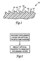
- Figure 1 is a cross-sectional diagram of a typical fresnel lens die 10 including optical facets 12 separated by risers 14.
- the risers 14 provide the vertical displacement between optical facets 12 that is required to produce a substantially planar lens from the die 10.
- the die 10 is typically manufactured from metals such as brass, copper, nickel, etc.
- the die 10 when the die 10 is a "negative" of the desired fresnel lens, it can be used directly to produce a fresnel lens or, alternatively, a "mother” can be electroformed from the die 10 and stampers (also a negative of the desired lens) can then be electroformed from the mothers to produce fresnel lenses. Where the die 10 is a "positive" of the desired fresnel lens, an electroformed copy will be a negative of the lens and can be used to form the desired fresnel lens.
- the method according to the present invention can be used to provide the desired diffuse risers 14.
- the basic steps of the method are depicted in the block diagram of Figure 2.
- a diffusing layer is deposited over the entire surface of the die 10, including the optical facets 12 and risers 14.
- the optical facets 12 are processed to remove the diffusing layer and restore their specular finish while leaving the diffusing layer on the risers 14.
- the processing typically involves machining, or recutting, the optical facets 12 to remove the diffusing layer from them while leaving the diffusing layer on the risers 14.
- the diffusing layer is formed by electrodepositing a metal such as copper, nickel, zinc, tin, cobalt, etc. Combinations of one or more of the metals may also be used for the diffusing layer.
- the method of depositing the diffusing layer is electroplating in a bath of electrolyte solution.
- the bath is substantially free of grain refiners to enhance the diffusing properties of the diffusing layer. If an electrolyte solution prepared with grain refiners is to be used, the bath can be filtered through activated carbon to remove the grain refiners.
- the bath can be heated or allowed to heat up during processing to cause degeneration of any grain refiners in the solution.
- the grain refiners degenerate at elevated temperatures because they are typically organic and, thus, susceptible to heat degeneration.
- Temperatures of the bath useful in connection with the present invention can range from about 30°C or greater, more preferably about 35°C or greater, and even more preferably about 40°C or greater.
- the current density of the plating process can also play a role in the uniformity of the diffusing layer on the surface of the die. It is preferred that the current density be about 0.022 amps/cm 2 (20 amps/ft 2 ) or less, more preferably about 0.016 amps/cm 2 (15 amps/ft 2 ) or less, and even more preferably about 0. 011 amps/cm 2 (10 amps/ft 2 ) or less. It will be understood that the desire for plating speed, i.e., rate of deposition, will typically be balanced with plating uniformity.
- the die 10 can then be electroformed or otherwise duplicated to form mothers or stampers if desired.
- the die 10 itself could be used to form a fresnel lens.
- the diffusing layer deposited on the die 10 is matte copper.
- the process used to electrodeposit the matte copper is described in Example 1 below.
- the matte finish is provided by electroplating the die 10 in a bath that is substantially free of grain refiners. This produces a finish in the matte copper that is grainier than typically found in electrodeposited copper layers.
- a fresnel lens die master having a surface area of about 0.2 square meters manufactured of nickel was electroplated with a diffusing layer of matte copper according to the following procedure.
- An electroplating solution was prepared including copper sulfate (0.21 kg/liter of solution) (copper sulfate pentahydrate sold as Triangle Brand by Phelps Dodge Refining Corporation, El Paso, Texas), sulfuric acid (0.061 kg/liter of solution) (96% pure, reagent grade), chloride (50 PPM), and a surfactant (1 liter of 10% Duponal ME per 757 liters of solution, available from DuPont). The balance of the solution was distilled water. The solution was filtered through a 1 micrometer filter and activated carbon to remove impurities before plating.
- the die Before electroplating, the die was soaked in MEK/acetone solvent bath to remove oils and other contaminants on the surface of the die. The die was then power washed with a 20% AdvanageTM cleaner solution (AdvanageTM is available from Austin Diversified Products, Inc., Harvey, Illinois). After power washing, the die was maintained wet in a solution of 20% H 2 SO 4 and 5% AdvanageTM (balance distilled water) while it was mounted on the electroplating equipment.
- AdvanageTM cleaner solution AdvancedTM is available from Austin Diversified Products, Inc., Harvey, Illinois.
- the nickel die was first reverse plated for one minute at 25 amps with the die being the anode. Plating was then commenced after reversing polarity (i.e., the die was the cathode) and plating was carried out for about two hours at 20 amps for a total of 42 amp-hours.
- the electroplating solution was held at a temperature of 35°C, the die was rotated in the solution at 3 0 revolutions per minute, the electroplating solution was agitated with a mixer and the solution was recirculated through a 1 micrometer filter at a rate of 114 liters per minute.
- the resulting die appeared uniformly coated with a layer of matte copper.
- a second nickel die essentially identical to the die used in Example 1 was electroplated under the same conditions as set out in Example 1, except that the electroplating was carried out at 42 amps for a total of 42 amp-hours.
- the finished die did not appear as uniformly plated as the die produced according to Example 1.
- a copper die with a similar pattern and size as the nickel dies used in Examples 1 and 2 was plated with matte copper according to the process described in Example 1 with the following exceptions: the temperature of the bath during plating was 40°C; the plating was carried out for about 40 minutes at 13-15 amps for a total of 11 amp-hours.
- the resulting die had a uniform satin appearance.
- a nickel electroform was produced using the die, virtually none of the matte copper was removed by the electroformed copy.
- a copper die was electroformed according to Example 3, with the following exception: during plating, a mask was placed with the logo of Minnesota Mining and Manufacturing Company ("3M") over the die for about one-half of the total plating time.
- the logo was provided of a magnetic material that adhered to the nickel substrate on which the copper surface was mounted. Because no further plating occurred in the area underneath the mask after its placement, the plating thickness was reduced in the area covered by the mask, resulting in the logo being transferred to the die. Lenses that were ultimately manufactured from this die also exhibited the logo when viewed from an angle, i.e., not normal to the plane of the lens.
Landscapes
- Physics & Mathematics (AREA)
- General Physics & Mathematics (AREA)
- Optics & Photonics (AREA)
- Electroplating Methods And Accessories (AREA)
- Moulds For Moulding Plastics Or The Like (AREA)
- Overhead Projectors And Projection Screens (AREA)
- Shaping Of Tube Ends By Bending Or Straightening (AREA)
- Casting Or Compression Moulding Of Plastics Or The Like (AREA)
- Eyeglasses (AREA)
- Optical Elements Other Than Lenses (AREA)
Description
Claims (12)
- A method of providing diffusing risers on a fresnel lens die having a plurality of optical facets, wherein adjacent optical facets are separated by a riser, the method comprising the steps of:a) depositing a diffusing layer on the plurality of optical facets and the risers, wherein the depositing comprises electrodepositing a layer of metal chosen from the group consisting of copper, nickel, zinc, cobalt, tin, and combinations thereof, and further wherein the electrodepositing is performed in a bath substantially free of grain refiners; andb) selectively removing the diffusing layer from the plurality of optical facets, wherein the diffusing layer remains substantially intact on the risers.
- A method according to claim 1, wherein the step of depositing further comprises depositing the diffusing layer on a die having generally concentric optical facets.
- A method according to claim 1, wherein the step of depositing further comprises depositing the diffusing layer on a die having generally parallel optical facets.
- A method according to any of claims 1-3, further comprising a step of passing the bath through activated charcoal.
- A method according to any of claims 1-4, further comprising a step of heating the bath to a temperature of about 30°C or higher.
- A method according to any of claims 1-4, further comprising a step of heating the bath to a temperature of about 35°C or higher.
- A method according to any of claims 1-4, further comprising a step of heating the bath to a temperature of about 40°C or higher.
- A method according to any of claims 1-7, further comprising masking selected portions of the risers during the step of depositing the diffusing layer.
- A method according to any of claims 1-7, further comprising masking selected portions of the risers during a portion of the time during which the step of depositing is being performed.
- A method according to any of claims 1-9, wherein the step of depositing further comprises passing electrical energy through the die having a current density of about 0.022 amps/cm2 or less.
- A method according to any of claims 1-9, wherein the step of depositing further comprises passing electrical energy through the die having a current density of about 0.016 amps/cm2 or less.
- A method according to any of claims 1-9, wherein the step of depositing further comprises passing electrical energy through the die having a current density of about 0.011 amps/cm2 (10 amps/ft2) or less.
Applications Claiming Priority (3)
| Application Number | Priority Date | Filing Date | Title |
|---|---|---|---|
| US08/654,356 US5997709A (en) | 1996-05-28 | 1996-05-28 | Method of providing diffuse risers on a fresnel lens die |
| US654356 | 1996-05-28 | ||
| PCT/US1997/008816 WO1997045758A1 (en) | 1996-05-28 | 1997-05-27 | Method of providing diffuse risers on a fresnel lens die |
Publications (2)
| Publication Number | Publication Date |
|---|---|
| EP0901643A1 EP0901643A1 (en) | 1999-03-17 |
| EP0901643B1 true EP0901643B1 (en) | 2003-12-03 |
Family
ID=24624532
Family Applications (1)
| Application Number | Title | Priority Date | Filing Date |
|---|---|---|---|
| EP97924797A Expired - Lifetime EP0901643B1 (en) | 1996-05-28 | 1997-05-27 | Method of providing diffuse risers on a fresnel lens die |
Country Status (9)
| Country | Link |
|---|---|
| US (1) | US5997709A (en) |
| EP (1) | EP0901643B1 (en) |
| JP (1) | JP4009750B2 (en) |
| KR (1) | KR20000015950A (en) |
| CN (1) | CN1219243A (en) |
| AU (1) | AU729770B2 (en) |
| DE (1) | DE69726570T2 (en) |
| TW (1) | TW340910B (en) |
| WO (1) | WO1997045758A1 (en) |
Families Citing this family (14)
| Publication number | Priority date | Publication date | Assignee | Title |
|---|---|---|---|---|
| US20100302479A1 (en) * | 1996-03-21 | 2010-12-02 | Aronson Joseph T | Optical article |
| JP2002166425A (en) * | 2000-11-30 | 2002-06-11 | Dainippon Printing Co Ltd | Mold duplicating method and property judging method |
| US6649328B2 (en) * | 2001-01-15 | 2003-11-18 | Kuraray Co., Ltd. | Method for manufacture of molding die for Fresnel lens sheet |
| US7690814B2 (en) * | 2005-03-10 | 2010-04-06 | Honeywell International Inc. | Luminaire with a one-sided diffuser |
| US20070125655A1 (en) * | 2005-12-02 | 2007-06-07 | Buckley Paul W | Electroform, methods of making electroforms, and products made from electroforms |
| US20070125652A1 (en) * | 2005-12-02 | 2007-06-07 | Buckley Paul W | Electroform, methods of making electroforms, and products made from electroforms |
| US20070125653A1 (en) * | 2005-12-02 | 2007-06-07 | Coyle Dennis J | Multilayer electroform, methods of making multilayer electroforms, and products made therefrom |
| US20070125651A1 (en) * | 2005-12-02 | 2007-06-07 | Buckley Paul W | Electroform, methods of making electroforms, and products made from electroforms |
| US20070125654A1 (en) * | 2005-12-02 | 2007-06-07 | Buckley Paul W | Electroform, methods of making electroforms, and products made from electroforms |
| US20070126148A1 (en) * | 2005-12-02 | 2007-06-07 | General Electric Company | Microstructured embossing drum and articles made therefrom |
| US20070126144A1 (en) * | 2005-12-02 | 2007-06-07 | Yadong Jin | Polish/texture thermoplastic film and method for making the same |
| US20070125248A1 (en) * | 2005-12-02 | 2007-06-07 | Coyle Dennis J | Embossing drum system with removable outer sleeve and methods of use |
| WO2014065823A1 (en) | 2012-10-26 | 2014-05-01 | Empire Technology Development Llc | Illumination control |
| KR102010740B1 (en) * | 2013-03-05 | 2019-08-14 | 현대모비스 주식회사 | Optical Lens |
Family Cites Families (12)
| Publication number | Priority date | Publication date | Assignee | Title |
|---|---|---|---|---|
| US3712707A (en) * | 1970-02-27 | 1973-01-23 | Gen Electric | Composite back projection screen and method of forming |
| US4114983A (en) * | 1977-02-18 | 1978-09-19 | Minnesota Mining And Manufacturing Company | Polymeric optical element having antireflecting surface |
| US4229085A (en) * | 1977-03-10 | 1980-10-21 | Canon Kabushiki Kaisha | Film reader |
| JPS56111804A (en) * | 1980-02-09 | 1981-09-03 | Dainippon Printing Co Ltd | Manufacture of body differing in optical property according to direction |
| US4334966A (en) * | 1981-05-19 | 1982-06-15 | Mcgean Chemical Company, Inc. | Method of copper plating gravure cylinders |
| JPS60230601A (en) * | 1984-05-01 | 1985-11-16 | Masayasu Negishi | Treatment of film |
| US4781801A (en) * | 1987-02-03 | 1988-11-01 | Mcgean-Rohco, Inc. | Method of copper plating gravure rolls |
| FR2617510B1 (en) * | 1987-07-01 | 1991-06-07 | Snecma | METHOD FOR THE ELECTROLYTIC CODEPOSITION OF A NICKEL-COBALT MATRIX AND CERAMIC PARTICLES AND COATING OBTAINED |
| US4842633A (en) * | 1987-08-25 | 1989-06-27 | Matsushita Electric Industrial Co., Ltd. | Method of manufacturing molds for molding optical glass elements and diffraction gratings |
| DE3835567A1 (en) * | 1988-10-19 | 1989-11-02 | Peter Nawrath | Process for producing non-glare Fresnel lenses from acrylic and other transparent materials which can be deformed by press-moulding or injection-moulding |
| JP3147481B2 (en) * | 1992-04-21 | 2001-03-19 | 松下電器産業株式会社 | Mold for forming glass diffraction grating, method for manufacturing the same, and method for manufacturing glass diffraction grating |
| US5317349A (en) * | 1993-06-29 | 1994-05-31 | Minnesota Mining And Manufacturing Company | Overhead projector with achromatic fresnel lens |
-
1996
- 1996-05-28 US US08/654,356 patent/US5997709A/en not_active Expired - Lifetime
-
1997
- 1997-05-27 EP EP97924797A patent/EP0901643B1/en not_active Expired - Lifetime
- 1997-05-27 KR KR1019980709507A patent/KR20000015950A/en not_active Application Discontinuation
- 1997-05-27 AU AU30110/97A patent/AU729770B2/en not_active Ceased
- 1997-05-27 JP JP54279297A patent/JP4009750B2/en not_active Expired - Fee Related
- 1997-05-27 CN CN97194811A patent/CN1219243A/en active Pending
- 1997-05-27 DE DE69726570T patent/DE69726570T2/en not_active Expired - Lifetime
- 1997-05-27 WO PCT/US1997/008816 patent/WO1997045758A1/en active IP Right Grant
- 1997-06-03 TW TW086107599A patent/TW340910B/en active
Also Published As
| Publication number | Publication date |
|---|---|
| JP2000511305A (en) | 2000-08-29 |
| TW340910B (en) | 1998-09-21 |
| CN1219243A (en) | 1999-06-09 |
| EP0901643A1 (en) | 1999-03-17 |
| WO1997045758A1 (en) | 1997-12-04 |
| US5997709A (en) | 1999-12-07 |
| AU3011097A (en) | 1998-01-05 |
| DE69726570D1 (en) | 2004-01-15 |
| JP4009750B2 (en) | 2007-11-21 |
| DE69726570T2 (en) | 2004-11-11 |
| AU729770B2 (en) | 2001-02-08 |
| KR20000015950A (en) | 2000-03-25 |
Similar Documents
| Publication | Publication Date | Title |
|---|---|---|
| EP0901643B1 (en) | Method of providing diffuse risers on a fresnel lens die | |
| US4781799A (en) | Electroforming apparatus and process | |
| US4568431A (en) | Process for producing electroplated and/or treated metal foil | |
| CN104911676B (en) | Alkaline electro plating bath with filtration membrane | |
| US4549950A (en) | Systems for producing electroplated and/or treated metal foil | |
| JPS62103386A (en) | Electroforming method | |
| US6607614B1 (en) | Amorphous non-laminar phosphorous alloys | |
| CN1524136A (en) | Electrolyte media for the deposition of tin alloys and methods for depositing tin alloys | |
| CA2252905C (en) | Method of providing diffuse risers on a fresnel lens die | |
| CN1831205B (en) | Metal structure and method of its production | |
| US4532014A (en) | Laser alignment system | |
| JPH05230685A (en) | Electrocast products with high dimensional stability | |
| US5385660A (en) | Dendritic growth assisted electroform separation | |
| US5543028A (en) | Electroforming semi-step carousel, and process for using the same | |
| JPH08258051A (en) | Production of lens mold | |
| US20020079026A1 (en) | Process for preparing novel amorphous non-laminar phosphate alloys | |
| WO2007011642A1 (en) | Tool and method of making and using the same | |
| KR910002570B1 (en) | High performance electrodeposited chromium layers | |
| EP0181430A1 (en) | Systems for producing electroplated and/or treated metal foil | |
| MXPA98009772A (en) | Procedure for providing of coulders or diffused realces to a fresh lens mold | |
| EP1032719B1 (en) | Amorphous non-laminar nickel and/or cobalt phosphorous alloys, their process of manufacture and uses | |
| Rodia | Precision electroforming for optical disk manufacturing | |
| Hung | Optimization on hardness and internal stress of micro-electroformed NiCo/nano-Al2O3 composites with the constraint of low surface roughness | |
| US20070125653A1 (en) | Multilayer electroform, methods of making multilayer electroforms, and products made therefrom | |
| CN1427093A (en) | Metal template |
Legal Events
| Date | Code | Title | Description |
|---|---|---|---|
| PUAI | Public reference made under article 153(3) epc to a published international application that has entered the european phase |
Free format text: ORIGINAL CODE: 0009012 |
|
| 17P | Request for examination filed |
Effective date: 19981217 |
|
| AK | Designated contracting states |
Kind code of ref document: A1 Designated state(s): DE ES FR GB IT |
|
| 17Q | First examination report despatched |
Effective date: 20010801 |
|
| GRAH | Despatch of communication of intention to grant a patent |
Free format text: ORIGINAL CODE: EPIDOS IGRA |
|
| GRAS | Grant fee paid |
Free format text: ORIGINAL CODE: EPIDOSNIGR3 |
|
| GRAA | (expected) grant |
Free format text: ORIGINAL CODE: 0009210 |
|
| AK | Designated contracting states |
Kind code of ref document: B1 Designated state(s): DE ES FR GB IT |
|
| PG25 | Lapsed in a contracting state [announced via postgrant information from national office to epo] |
Ref country code: IT Free format text: LAPSE BECAUSE OF FAILURE TO SUBMIT A TRANSLATION OF THE DESCRIPTION OR TO PAY THE FEE WITHIN THE PRESCRIBED TIME-LIMIT;WARNING: LAPSES OF ITALIAN PATENTS WITH EFFECTIVE DATE BEFORE 2007 MAY HAVE OCCURRED AT ANY TIME BEFORE 2007. THE CORRECT EFFECTIVE DATE MAY BE DIFFERENT FROM THE ONE RECORDED. Effective date: 20031203 Ref country code: ES Free format text: LAPSE BECAUSE OF FAILURE TO SUBMIT A TRANSLATION OF THE DESCRIPTION OR TO PAY THE FEE WITHIN THE PRESCRIBED TIME-LIMIT Effective date: 20031203 |
|
| REG | Reference to a national code |
Ref country code: GB Ref legal event code: FG4D |
|
| REF | Corresponds to: |
Ref document number: 69726570 Country of ref document: DE Date of ref document: 20040115 Kind code of ref document: P |
|
| ET | Fr: translation filed | ||
| PLBE | No opposition filed within time limit |
Free format text: ORIGINAL CODE: 0009261 |
|
| STAA | Information on the status of an ep patent application or granted ep patent |
Free format text: STATUS: NO OPPOSITION FILED WITHIN TIME LIMIT |
|
| 26N | No opposition filed |
Effective date: 20040906 |
|
| PGFP | Annual fee paid to national office [announced via postgrant information from national office to epo] |
Ref country code: GB Payment date: 20070525 Year of fee payment: 11 |
|
| PGFP | Annual fee paid to national office [announced via postgrant information from national office to epo] |
Ref country code: FR Payment date: 20070517 Year of fee payment: 11 |
|
| GBPC | Gb: european patent ceased through non-payment of renewal fee |
Effective date: 20080527 |
|
| REG | Reference to a national code |
Ref country code: FR Ref legal event code: ST Effective date: 20090119 |
|
| PG25 | Lapsed in a contracting state [announced via postgrant information from national office to epo] |
Ref country code: FR Free format text: LAPSE BECAUSE OF NON-PAYMENT OF DUE FEES Effective date: 20080602 |
|
| PG25 | Lapsed in a contracting state [announced via postgrant information from national office to epo] |
Ref country code: GB Free format text: LAPSE BECAUSE OF NON-PAYMENT OF DUE FEES Effective date: 20080527 |
|
| PGFP | Annual fee paid to national office [announced via postgrant information from national office to epo] |
Ref country code: DE Payment date: 20100519 Year of fee payment: 14 |
|
| REG | Reference to a national code |
Ref country code: DE Ref legal event code: R119 Ref document number: 69726570 Country of ref document: DE |
|
| REG | Reference to a national code |
Ref country code: DE Ref legal event code: R119 Ref document number: 69726570 Country of ref document: DE |
|
| PG25 | Lapsed in a contracting state [announced via postgrant information from national office to epo] |
Ref country code: DE Free format text: LAPSE BECAUSE OF NON-PAYMENT OF DUE FEES Effective date: 20111130 |