EP0901081A2 - A digital signal processor with peripheral devices and external interfaces - Google Patents
A digital signal processor with peripheral devices and external interfaces Download PDFInfo
- Publication number
- EP0901081A2 EP0901081A2 EP98305453A EP98305453A EP0901081A2 EP 0901081 A2 EP0901081 A2 EP 0901081A2 EP 98305453 A EP98305453 A EP 98305453A EP 98305453 A EP98305453 A EP 98305453A EP 0901081 A2 EP0901081 A2 EP 0901081A2
- Authority
- EP
- European Patent Office
- Prior art keywords
- data
- dma
- circuitry
- cpu
- address
- Prior art date
- Legal status (The legal status is an assumption and is not a legal conclusion. Google has not performed a legal analysis and makes no representation as to the accuracy of the status listed.)
- Granted
Links
Images
















Classifications
-
- G—PHYSICS
- G06—COMPUTING OR CALCULATING; COUNTING
- G06F—ELECTRIC DIGITAL DATA PROCESSING
- G06F9/00—Arrangements for program control, e.g. control units
- G06F9/06—Arrangements for program control, e.g. control units using stored programs, i.e. using an internal store of processing equipment to receive or retain programs
- G06F9/30—Arrangements for executing machine instructions, e.g. instruction decode
- G06F9/30003—Arrangements for executing specific machine instructions
- G06F9/30007—Arrangements for executing specific machine instructions to perform operations on data operands
- G06F9/3001—Arithmetic instructions
-
- G—PHYSICS
- G06—COMPUTING OR CALCULATING; COUNTING
- G06F—ELECTRIC DIGITAL DATA PROCESSING
- G06F15/00—Digital computers in general; Data processing equipment in general
- G06F15/76—Architectures of general purpose stored program computers
- G06F15/78—Architectures of general purpose stored program computers comprising a single central processing unit
- G06F15/7828—Architectures of general purpose stored program computers comprising a single central processing unit without memory
- G06F15/7832—Architectures of general purpose stored program computers comprising a single central processing unit without memory on one IC chip (single chip microprocessors)
-
- G—PHYSICS
- G06—COMPUTING OR CALCULATING; COUNTING
- G06F—ELECTRIC DIGITAL DATA PROCESSING
- G06F9/00—Arrangements for program control, e.g. control units
- G06F9/06—Arrangements for program control, e.g. control units using stored programs, i.e. using an internal store of processing equipment to receive or retain programs
- G06F9/30—Arrangements for executing machine instructions, e.g. instruction decode
- G06F9/30003—Arrangements for executing specific machine instructions
- G06F9/30076—Arrangements for executing specific machine instructions to perform miscellaneous control operations, e.g. NOP
- G06F9/30083—Power or thermal control instructions
-
- G—PHYSICS
- G06—COMPUTING OR CALCULATING; COUNTING
- G06F—ELECTRIC DIGITAL DATA PROCESSING
- G06F9/00—Arrangements for program control, e.g. control units
- G06F9/06—Arrangements for program control, e.g. control units using stored programs, i.e. using an internal store of processing equipment to receive or retain programs
- G06F9/30—Arrangements for executing machine instructions, e.g. instruction decode
- G06F9/30098—Register arrangements
-
- G—PHYSICS
- G06—COMPUTING OR CALCULATING; COUNTING
- G06F—ELECTRIC DIGITAL DATA PROCESSING
- G06F9/00—Arrangements for program control, e.g. control units
- G06F9/06—Arrangements for program control, e.g. control units using stored programs, i.e. using an internal store of processing equipment to receive or retain programs
- G06F9/30—Arrangements for executing machine instructions, e.g. instruction decode
- G06F9/30098—Register arrangements
- G06F9/30101—Special purpose registers
Definitions
- This invention relates to microprocessors, and particularly relates to microprocessor integrated circuits which include an on-chip peripheral devices and various external interface ports.
- Microprocessor designers have increasingly endeavored to improve performance in various microprocessors by increasing clock speeds and adding parallelism.
- Large blocks of random access memory (RAM) are included within the microprocessor for data storage and for program storage in order to reduce memory access times.
- RAM random access memory
- Various types of input/output devices are included within a microprocessor integrated circuit in order to reduce total system chip count and cost.
- Serial ports are an example of a class of input/output devices that are commonly included with microprocessors.
- An object of the present invention is to provide improvements in the operation and control of on-chip peripheral devices and external interfaces for microprocessor integrated circuits.
- one form of the invention is a data processing device including a central processing unit (CPU) for executing instructions, a memory circuit connected to the central processing unit for storing the instructions which are executed by the CPU, and a serial port interface circuit connected to the CPU, operable to transmit and receive data with dual phase frames, wherein each phase has a different set of parameters.
- CPU central processing unit
- memory circuit connected to the central processing unit for storing the instructions which are executed by the CPU
- serial port interface circuit connected to the CPU, operable to transmit and receive data with dual phase frames, wherein each phase has a different set of parameters.
- a data processing device including a central processing unit (CPU) for executing instructions, a memory controller connected to said central processing unit, and a memory circuit connected to said memory controller.
- the data processing device may further include an external memory interface circuit connected to said memory controller.
- the data processing device may further include a host port interface connected to said direct memory access controller.
- the data processing device may further include a peripheral bus controller connected to said memory controller, and an external memory interface controller connected to said peripheral bus controller.
- the data processing device may further include at least one external signal for defining the type of memory located at a reset address for said central processing unit.
- the data processing device may further include at least one external signal for identifying the size and location of said memory circuit.
- the data processing device may further include a programmable timer connected to said peripheral bus controller.
- the data processing device may further include a programmable phase-locked loop circuit for providing clock signals to said central processing unit.
- the data processing device may further include a power down circuit for programmably preventing clocking signals from reaching preselected portions of said device.
- Another form of the invention is a data processing device including a central processing unit operable to execute software instructions stored in a program memory circuit connected to the central processing unit, a memory circuit operable to store data to be processed by the processing device, a direct memory access (DMA) controller having read address circuitry and write address circuitry, operable to transfer data from or to the memory circuit, the DMA controller further having DMA interrupt circuitry operable to interrupt the central processing unit.
- the device may further include a peripheral device having address generation circuitry operable transfer data to or from the memory circuit.
- the device may further include auxiliary channel control circuitry operable to cause the peripheral device to transfer a first data word to the memory circuit using the address generation circuitry of the peripheral device and to interrupt the central processor using the DMA interrupt circuitry of the DMA controller.
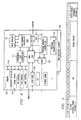
- FIG. 1A is a block diagram of a microprocessor 1 which includes an embodiment of the present invention.
- Microprocessor 1 is a VLIW digital signal processor ("DSP").
- DSP VLIW digital signal processor
- Figure 1A only shows those portions of microprocessor 1 that are relevant to an understanding of an embodiment of the present invention. Details of general construction for DSPs are well known, and may be found readily elsewhere.
- U.S. Patent 5,072,418 issued to Frederick Boutaud, et al describes a DSP in detail and is incorporated herein by reference.
- U.S. Patent 5,329,471 issued to Gary Swoboda, et al describes in detail how to test and emulate a DSP and is incorporated herein by reference. Details of portions of microprocessor 1 relevant to an embodiment of the present invention are explained in sufficient detail hereinbelow, so as to enable one of ordinary skill in the microprocessor art to make and use the invention.
- CPU 10 central processing unit
- CPU 10 data memory 22, program memory 23, peripherals 60 and an external memory interface (EMIF) with a direct memory access (DMA) 61.
- CPU 10 further has an instruction fetch/decode unit 10a-c , a plurality of execution units, including an arithmetic and load/store unit D1, a multiplier M1, an ALU/shifter unit S1, an arithmetic logic unit (“ALU") L1, a shared multiport register file 20a from which data are read and to which data are written.
- Decoded instructions are provided from the instruction fetch/decode unit 10a-c to the functional units D1, M1, S1, and L1 over various sets of control lines which are not shown.
- Data are provided to/from the register file 20a from/to to load/store units D1 over a first set of busses 32a, to multiplier M1 over a second set of busses 34a, to ALU/shifter unit S1 over a third set of busses 36a and to ALU L1 over a fourth set of busses 38a.
- Data are provided to/from the memory 22 from/to the load/store units D1 via a fifth set of busses 40a. Note that the entire data path described above is duplicated with register file 20b and execution units D2, M2, S2, and L2. Instructions are fetched by fetch unit 10a from instruction memory 23 over a set of busses 41.
- Emulation unit 50 provides access to the internal operation of integrated circuit 1 which can be controlled by an external test system 51.
- memory 22 and memory 23 are shown in Figure 1 to be a part of a microprocessor 1 integrated circuit, the extent of which is represented by the box 42.
- the memories 22-23 could just as well be external to the microprocessor 1 integrated circuit 42, or part of it could reside on the integrated circuit 42 and part of it be external to the integrated circuit 42. Also, an alternate number of execution units can be used.
- RAM 70 Random Access Memory
- ROM Read Only Memory
- Disk 72 Disk 72
- Bus 73 is connected to an External Memory Interface (EMIF) which is part of functional block 61 within microprocessor 42.
- a Direct Memory Access (DMA) controller is also included within block 61.
- the DMA controller is generally used to move data between memory and peripherals within microprocessor 1 and memory and peripherals which are external to microprocessor 1. Data can be transferred from block 61 to program memory 23 via bus 43; data can be transferred to/from data memory 22 via bus 44.
- Other types of peripherals, such as timer 82 are connected via host port bus 80.
- a bus interface is contained within block 60 for host port bus 80.
- U.S. Patent 5,072,4108 which was incorporated by reference herein, particularly with reference to Figures 2-18 of U.S. Patent 5,072,418.
- a microprocessor incorporating an aspect of the present invention to improve performance or reduce cost can be used to further improve the systems described in U.S. Patent 5,072,418.
- Such systems include, but are not limited to, industrial process controls, automotive vehicle systems, motor controls, robotic control systems, satellite telecommunication systems, echo canceling systems, modems, video imaging systems, speech recognition systems, vocoder-modem systems with encryption, and such.
- a description of various architectural features of the microprocessor of Fig. 1A is provided in co-assigned European Patent application Number 981011291.7.
- a description of a complete set of instructions for the microprocessor of Fig. 1A is also provided in this co-assigned application.
- FIGS. 1B and 1C are a more detailed block diagram of the microprocessor of Fig. 1A.
- Multi-channel Serial Port 120 is connected to peripheral bus 110.
- FIG. 2 is a block diagram of the execution units and register files of the microprocessor of Fig. 1A and shows a more detailed view of the buses connecting the various functional blocks.
- Bus 40a has an address bus DA1 which is driven by mux 200a. This allows an address generated by either load/store unit D1 12a or D2 12b to provide an address for loads or stores for register file 20a.
- Data Bus LD1 loads data from an address in memory 22 specified by address bus DA1 to a register in load unit D1 12a.
- Unit D1 12a may manipulate the data provided prior to storing it in register file 20a.
- data bus ST1 stores data from register file 20a to memory 22.
- Load/store unit D1 12a performs the following operations: 32-bit add, subtract, linear and circular address calculations.
- Load/store unit D2 12b operates similarly to unit D1 12a, with the assistance of mux 200b for selecting an address.
- ALU unit L1 18a performs the following types of operations: 32/40 bit arithmetic and compare operations; left most 1, 0, bit counting for 32 bits; normalization count for 32 and 40 bits; and logical operations.
- ALU L1 18a has input srcl for a 32 bit source operand and input src2 for a second 32 bit source operand.
- Input msb_src is an 8 bit value used to form 40 bit source operands.
- ALU L1 18a has an output dst for a 32 bit destination operands.
- Output msb_dst is an 8 bit value used to form 40 bit destination operands.
- Two 32 bit registers in register file 20a are concatenated to hold a 40 bit operand.
- Mux 211 is connected to input srcl and allows a 32 bit operand to be obtained from register file 20a via bus 38a or from register file 20b via bus 210.
- Mux 212 is connected to input src2 and allows a 32 bit operand to be obtained from register file 20a via bus 38a or from register file 20b via bus 210.
- ALU unit L2 18b operates similarly to unit L1 18a.
- ALU/shifter unit S1 16a performs the following types of operations: 32 bit arithmetic operations; 32/40 bit shifts and 32 bit bit-field operations; 32 bit logical operations; branching; and constant generation.
- ALU S1 16a has input srcl for a 32 bit source operand and input src2 for a second 32 bit source operand.
- Input msb_src is an 8 bit value used to form 40 bit source operands.
- ALU S1 16a has an output dst for a 32 bit destination operands.
- Output msb_dst is an 8 bit value used to form 40 bit destination operands.
- Mux 213 is connected to input src2 and allows a 32 bit operand to be obtained from register file 20a via bus 36a or from register file 20b via bus 210.
- ALU unit S2 16b operates similarly to unit S1 16a, but can additionally perform register transfers to/from the control register file 102.
- Multiplier M1 14a performs 16 x 16 multiplies.
- Multiplier M1 14a has input srcl for a 32 bit source operand and input src2 for a 32 bit source operand.
- Multiplier M1 14a dst for a 32 bit destination operands.
- Mux 214 is connected to input src2 and allows a 32 bit operand to be obtained from register file 20a via bus 34a or from register file 20b via bus 210.
- Multiplier M2 14b operates similarly to multiplier M1 14a.
- Figure 3A and 3B shows two memory maps for the microprocessor of Fig. 1A.
- the memory is byte addressable and its total address range is 4G bytes (corresponding to a 32-bit internal address).
- the memory map is divided between the internal program memory 23, internal data memory 22 and three external memory spaces and internal peripheral space.
- a section of internal memory can be accessed by the host port interface (HPI) 60.
- HPI host port interface
- the internal memory consists of 512k bits of on-chip program/cache memory 23 and 512k bits of on-chip data memory 22.
- the program memory configurable as cache or program, is organized in 2k of 256-bit instruction fetch packets.
- the CPU 10 fetches all instructions one fetch packet at a time.
- the packets are processed at the maximum rate of eight 32-bit instructions per CPU cycle or at a minimum of one instruction per cycle.
- the internal data memory is byte addressable by the CPU (for reads as well as writes) and supports byte, half-word and full word transfers.
- the external memory is divided into three spaces - CEO, CE1 and CE2. Each has a dedicated chip enable signal that is asserted during data access to or from the corresponding space. Each external space has assigned a separate internal peripheral bus register that determines the shape of the read/write cycle when accessing asynchronous memory.
- CE0 and CE2 spaces can also interface to other types of memory.
- SBSRAM or SDRAM memory can be assigned to those two spaces by controlling signal levels on signal groups CE0_TYPE and CE2_TYPE (pins DC2-DC5) during Reset 76.
- External memory space CE1 can only interface to asynchronous memory. However, while spaces CE0 and CE2 are always 32-bit wide, the CE1 memory space can also be configured to the width of 8 or 16 bits by controlling signal levels on signal group CE1_WIDTH pins.
- the EMIF automatically packs bytes and half-words into words during read cycles - a feature typically used when booting from an 8- or 16-bit EPROM.
- the CE1 memory space can be used for ROM interfacing because ROM cycles are similar to asynchronous SRAM read cycles. Note, that while the CE1 space is the only external memory space that allows read cycles from 8- or 16-bit wide memory, read cycles from any external memory space can access byte or half-word sized data from 32-bit wide external memory.
- the EMIF data write cycles can transfer bytes, half-words or words to external memory as well, using BE_ control signals for byte selects.
- Data read cycles always latch all 4 bytes (all 4 BE_'s active) and the CPU then extracts the appropriate bytes internally if the data size is less then 32 bits.
- EMIF writes requested by the program memory controller 104 or the DMA 100/101 are always 32-bits wide, as opposed to 8-, 16-, or 32-bit transfers originated by the data memory controller 105.
- the internal program memory includes 64K bytes of RAM. This memory can include 2K 256-bit fetch packets which is equivalent to 16K 32-bit instructions.
- the CPU through the program memory controller has a single-cycle throughput 256-bit wide connection to internal program memory.
- Internal Program Memory Modes Program Mode AAPCC Value Description Mapped 000 Memory mapped. Cache Disabled. (Reset default.) Cache Enable 010 Cache accessed and updated on reads. Cache Freeze 011 Cache accessed but not updated on reads. Cache Bypass 100 Cache not accessed or updated on reads. AAAAA Reserved Other
- the internal program memory can be utilized in four modes selected by the Program Cache Control (PCC) field (bits 7--5) in the CPU Control and Status Register as shown in Table 1.
- PCC Program Cache Control
- the architecture of the cache is direct mapped.
- the 64K byte cache contains 2K fetch packets and thus 2K frames. (Often the terms block or line are used interchangeably with frame in cache terminology.)
- the width of the cache or frame size is 256-bits. Each frame in the cache is one fetch packet.
- FIG. 2-3 shows how the cache uses the fetch packet address from the CPU:
- a dedicated valid bit in the tag RAM indicates whether contents of that cache frame contains valid data. During a cache flush all these valid bits are cleared to indicate that no cache frames have valid data. Cache flushes only occurs when the transition of the cache from mapped mode to cache enabled mode.
- a cache miss is detected when the tag corresponding to the block offset of the fetch packet address requested by the CPU does not correspond to bits 25:16 of the fetch packet address or if the valid bit at that location is clear. If enabled, the cache loads the fetch packet into the corresponding frame, sets the valid bit, sets the tag to bits 25:16 of the requested address, and delivers this fetch packet to the CPU after all 8 instructions are available.
- the DMA can read and write to internal program memory when configured mapped mode.
- the Data Memory Controller connects:
- the peripheral bus controller performs arbitration between the CPU and DMA for the on-chip peripherals.
- the Data Memory Controller services all requests to internal memory as well as all CPU data requests.
- Figure 6 shows the directions of data flow as well as the master (requester) and slave (resource) relationships between the modules: CPU requests data reads and writes to:
- the 64K bytes of internal data RAM located from address 80000000 to 8000FFFF is organized as 4 blocks of 8K blocks of 16-bit halfwords. These blocks are organized in an interleave on 16-bit data with each block containing successive half-words. This interleave allows the two data ports and DMA to read neighboring 16-bit data elements without a resource conflict.
- Both the CPU and DMA can read and write 8-bit bytes, 16-bit halfwords, and 32-bit words.
- the data memory controller performs arbitration between the two CPU independently for each 16-bit block basis. The following data alignment restrictions apply:
- CPU clock refers to one period of the CPU input clock (CLKOUT1). (Not the device input clock).
- CPU cycle refers to the CPU processing one pipeline phase. All instructions in an execute packet proceed through one pipeline phase in one CPU cycle. However, CPU cycles may be extended to multiple CPU clocks by memory stalls. The extension of a CPU cycle to multiple CPU clocks is known as wait-states.
- Interleaved memory organization allows two CPU simultaneous memory accesses. In one CPU cycle, two simultaneous accesses to two different internal memory blocks occur without wait-states. Two simultaneous accesses to the same internal memory block stall the entire CPU pipeline for one CPU clock, providing two accesses in two CPU clocks. These rules apply regardless of whether the accesses are loads or stores. Loads and stores from the same execute packet are seen by the Data Memory Controller during the same CPU cycle. Loads and stores from future or previous CPU cycles do not cause waits for the internal data memory accesses in the current cycle. Thus, internal data memory access only causes wait-states when conflicts occur between instructions in the same fetch packet access the same 16-bit wide block. This condition is called an internal memory conflict.
- the Data Memory Controller stalls the CPU for one additional CPU clock, serializes the accesses, and performs each access separately. In prioritizing the two accesses, any load occurs before any store access. If both accesses are loads or both accesses are stores, the access from DA1 takes precedence over the access from DA2. Table 3 shows what access conditions cause internal memory conflicts given the when the CPU makes two data accesses (on DA1 and DA2).
- Table 3 may be used to determine DMA versus CPU conflicts. Assume that one axis represents the DMA access and the other represents the CPU access from one CPU data port. Then, perform this analysis again for the other data port. If both comparisons yield no conflict, then there is no CPU/DMA internal memory conflict. Here, the CPU access and DMA access occur in the background of each other. If either comparison yields a conflict, then there is a CPU/DMA internal memory conflict. In this case, the priority is resolved by the PRI bit of the DMA Channel as described later herein.
- LENDIAN Large ENDIAN
- Table 4 shows which bits of a data word in memory are loaded into which bits of a destination register for all possible CPU data loads from big or little endian data. The data in memory is assumed to be the same data that is in the register results from the LDW instruction in the first row.
- Table 5 shows which bits of a register are stored in which bits of a destination memory word for all possible CPU data stores from big and little endian data.
- the data in the source register is assumed to be the same data that is in the memory results from the STW instruction in the first row.
- the peripherals described herein are controlled by CPU and DMA through accesses of control registers.
- the CPU and DMA access these registers through the peripheral data bus.
- the DMA directly accesses the Peripheral Bus Controller, whereas CPU accesses it through the Data Memory Controller.
- the peripheral bus controller converts all peripheral bus accesses to word accesses. However, on read accesses both the CPU and DMA can extract the correct portions of the word to perform byte and halfword accesses properly. However, any side-effects by causing a peripheral control register read will occur regardless of which bytes are read. In contrast, if byte or halfword writes are performed only the values the CPU and DMA only provide correct values in the enabled bytes. The values guaranteed to be correct are shown in Table 5. Thus, undefined results will be written to the non-enabled bytes. If the user is not concerned about the values in the disabled bytes, this is acceptable. Otherwise, one should only access the peripheral registers via word accesses.
- An isolated peripheral bus controller accesses from the CPU causes 4 CPU wait states. These wait-states are inserted to allow pipeline registers to break-up the paths between traversing the on-chip distances between the CPU and peripherals as well as for arbitration time. On consecutive accesses, an accesses after the first only require 3 CPU wait-states due to the pipelined nature of the Data Memory Controller's interface to the peripheral bus controller.
- the Peripheral Bus Controller performs arbitration between the CPU and DMA for these functions. Like internal data access, the PRI bits in the DMA determine the priority between the CPU and the DMA. If a conflict occurs between the CPU (via the Data Memory Controller) the lower priority requester is held off until the higher priority requester completes all accesses to the peripheral bus controller.
- the peripheral bus is arbitrated as a single resource, thus the lower priority resource is blocked from accessing all peripherals, not just the one accessed by the higher priority requester.
- Direct Memory Access (DMA) Controller 143 transfers data between points in the memory map without intervention by the CPU.
- the DMA allows movement of data to and from internal memory, internal peripherals, or external devices to occur in the background of CPU operation.
- the DMA has four independent programmable channels allowing four different contexts for DMA operation. Each DMA channel can be independently configured to transfer data elements of different sizes: 8-bit bytes, 16-bit half-words, or 32-bit words.
- auxiliary allows the DMA to service request from a peripheral with address generation capability such as a host port interface.
- DMA 143 includes the following features, each of which will be described in following paragraphs:
- DMA 143 is controlled and configured by several memory mapped control registers.
- Table 7 and Table 8 show how the DMA control registers are mapped into CPU 10's memory space. These registers include the DMA Global Control and Data Registers as well as number of independent control registers for each channel.
- the DMA Global Data registers are usable as selected by channels for a variety of functions, as described in Table 9.
- Figure 7 illustrates a DMA Global Data Register.
- DMA Channel Control Registers are illustrated in Figure 8 and Figure 9.
- the DMA Channel Primary ( Figure 8) and Secondary Control Register ( Figure 9) contain bit fields that control each individual DMA Channel independently. These fields are described in Table 10 and Table 11, respectively.
- (SRC/DST) DIR 00b, no modification.
- (SRC/DST) DIR 01b, increment by element size in bytes
- (SRC/DST) DIR 10b, decrement by element size in bytes.
- (SRC/DST) DIR 11b, adjust using DMA Global Data Register selected by INDEX.
- RSYNC, WSYNC Read transfer/write transfer synchronization.
- (R/W)SYNC 00000b, no synchronization.
- TCINT Transfer Controller Interrupt .
- CNT RELOAD DMA Channel Transfer Counter Reload for Auto-Initialization and Multi-Frame Transfers
- CNT RELOAD 0, Reload with DMA Global Data Register 0
- CNT RELOAD 1
- Reload with DMA Global Data Register 1 INDEX Selects the DMA Global Data Register to use as a programmable index.
- DMA Channel Secondary Control Register Bit Fields Bit field Description SX COND DMA Condition. See 0 for FRAME COND description.
- FRAME IE See 0 for description.
- Requests are sent to one of four resources:
- the location of source and destination are computed at the beginning for a block transfer.
- the source address is assumed to point to the same one of these four spaces through out a block transfer. This constraint also applies to the destination address.
- Each DMA channel may be started independently either manually through direct CPU access or through auto-initialization. In addition, each DMA channel may be stopped or paused independently through direct CPU access.
- the DMA channel completes any the write transfers element transfers whose read transfer requests have completed. Also, if the DMA channel has all necessary read synchronization, one more element additional element transfer will be allowed to complete. Once paused, the value on STATUS is 10b.
- the DMA channel stops immediately and discards any data held internally from completed read transfers.
- the DMA can automatically reinitialize itself after completion of a block transfer.
- Some of the DMA control registers can be pre-loaded for the next block transfer through reload registers.
- Selected DMA Global Data registers act as the reload registers. Using this capability some of the parameters of the DMA channel can be set well in advance of the next block transfer. Auto-initialization allows:
- Continuous operation allows the CPU a long slack time during which it can reconfigure the DMA for the subsequent transfer. Normally, the CPU would have to reinitialize the DMA immediately after completion of the last write transfer in the current block transfer and before the first read synchronization for the next block transfer. In general, with the reload registers, it can reinitialize these values for the next block transfer anytime after the current block transfer begins.
- DMA Channel Reload Registers For auto-initialization, the successive block transfers are assumed to be similar. Thus, the reload values are only selectable for those registers that are modified during a block transfer: the transfer counter and address registers. Thus, the DMA Channel Transfer Counter as well as the DMA Channel Source and Destination Address Registers have associated reload registers, as selected by the associated RELOAD fields in the DMA Channel Primary Control Register (Table 10). The reload registers are stored in particular DMA Global Data registers.
- a DMA Global Data Register does not have to be dedicated to a value that was static during block transfer.
- a single channel may use the same value for multiple channel registers. For example, in split mode, the source and destination address maybe the same.
- multiple channels may use the same reload values. For example, two channels may have the same transfer count reload value.
- these registers Upon completion of a block transfer, these registers are reloaded with the associated reload register. Note that in the case of the DMA Channel Transfer Counter Register, reload occurs after the end of each frame transfer, not just after the end of the entire block transfer. The reload value for the DMA Channel Transfer Counter is necessary whenever multi-frame transfers are configured, not just when auto-initialization is enabled.
- the DMA may allow read transfers to get ahead of write transfers and provides the necessary buffering to facilitate this capability.
- the necessary reload at the end of blocks and frames occurs independently for the read (source) and write (destination) portions of the DMA Channel.
- the source and destination address are independently reloaded when the associated transmit or receive element transfers, respectively, complete a block transfer.
- the DMA Channel Transfer Counter Reload can only be re-written by the user after the next to last frame in the current block transfer completes. Otherwise, the new reload values would affect subsequent frame boundaries in the current block transfer. However, if the frame size is the same for the current and next block transfers, this restriction is not relevant. A fuller explanation of the DMA Channel Transfer Counter is provided in later paragraphs.
- Figure 10 illustrates a DMA Channel Transfer Counter.
- the DMA Channel Transfer Counter contains bit fields that represent the number of frames and the number of elements per frame to be transferred.
- Figure 11 shows how a DMA Global Data Register can be used as the reload value for the transfer counter.
- FRAME COUNT This 16-bit unsigned value sets the total number of frames in the block transfer. Thus, if a block transfer contains a single frame, this value should be set to its default of 1. The maximum number of frames per block transfer is 65535. This counter is decremented upon the completion of the last read transfer in a frame transfer. Once the last frame is transferred, the entire counter is reloaded with the DMA Global Data Register selected by the CNT RELOAD field in the DMA Channel Primary Control Register. Also note that initial values of 0 and 1 to FRAME COUNT have the same effect and a single frame will be transferred.
- ELEMENT COUNT This 16-bit unsigned value sets the number of elements per frame. This counter is decremented after the read transfer of each element. The maximum number of elements per frame transfer is 65535. Once the last element in each frame, is reached, ELEMENT COUNT is reloaded with the 16 LSBs of the DMA Global Data Register selected by the CNT RELOAD field in the DMA Channel Primary Control Register. This reloading is unaffected by auto-initialization mode. Before block transfer begins, the counter and selected DMA Global Data Register must be loaded with the same 16 LSBs to assure that the first and remaining frames have the same number of elements per frame. Also, in any multi-frame transfer, a reload value must be specified, not just when auto-initialization is enabled. If element count is initialized as 0, operation is undefined.
- Synchronization allows DMA transfers to be triggered by events such as interrupts from internal peripherals or external pins.
- events such as interrupts from internal peripherals or external pins.
- Three types of synchronization may be enabled for each channel:
- the DMA Channel Secondary Control Register (Table 11) contains STAT and CLR fields for read and write synchronization events.
- Latching of DMA Synchronization Events An inactive to active transition of the selected event is latched by each DMA channel. The occurrence of this transition causes the associated STAT field to be set in the DMA Channel Secondary Control register. Note that if no synchronization is selected the STAT bit is always read as 1. Also, note that a single event can trigger multiple actions.
- Frame synchronization is clears the RSYNC STAT field when the DMA completes the request for the first read transfer in the new frame.
- the DMA performs address computation for each read transfer and write transfer.
- the DMA allows creation of a variety of data structures. For example, the DMA can traverse an array striding through every n th element. Also, it can be programmed to effectively treat the various elements in a frame as coming from separate sources and group each source's data together.
- Figure 12 and Figure 13 illustrate the DMA Channel Source Address and Destination Address Registers, which hold the addresses for the next read transfer and write transfer, respectively.
- the SRC DIR and DST DIR fields can set the index to increment, to decrement, or to not effect the DMA Channel Source and Destination Address Registers, respectively. By default, these values are set to 00b to disable any incrementing or decrementing. If incrementing or decrementing is enabled, then address adjustment amount is by the element size in bytes. For example, if the source address is set to increment and 16-bit half-words are being transferred, then the address is incremented by 2 after each read transfer.
- the SRC DIR and DST DIR field can independently allow for selecting a particular DMA Global Data Register, illustrated in Figure 14, to determine the address adjustment.
- the particular DMA Global Data Register is selected via INDEX field in the DMA Channel Primary Control Register. Unlike basic address adjustment, this mode allows different adjustment amount depending on whether or not the element transfer is the last in the current frame.
- the normal adjustment value (ELEMENT INDEX) is contained in the 16 LSBs of the selected DMA Global Data Register.
- the adjustment value (FRAME INDEX) for the end of the frame is determined by the 16 MSBs of the selected DMA Global Data Register. Both these fields contain signed 16-bit values.
- the index amounts can range from - 32768 to 32767.
- Element Size, Alignment, and Endianness Using the ESIZE field in the DMA Channel Control Register, the user may configure the DMA to transfer 8-bit bytes, 16-bit halfwords, or 32-bit words on each transfer. The following registers and bit fields must be loaded with properly aligned values:
- the ELEMENT COUNT and FRAME COUNT can be used in conjunction to effectively allow single frame block transfers of greater than 65535 in size.
- the product of the element count and frame count can form a larger effective element count. The following must be performed:
- Table 13 and Table 14 show how this sorting works for this example. Sorting Example in Order of DMA Transfers Frame Element Address Post Adjustment 0 0 0x80000 000 +6 0 1 0x80000 006 +6 0 2 0x80000 00C +6 0 3 0x80000 012 -16 1 0 0x80000 002 +6 1 1 0x80000 008 +6 1 2 0x80000 00E +6 1 3 0x80000 014 -16 2 0 0x80000 004 +6 2 1 0x80000 00A +6 2 2 0x80000 010 +6 2 3 0x80000 016 -16 Sorting Grouping Ordered By Address Frame Element Address 0 0 0x80000000 1 0 0x80000002 2 0 0x80000004 0 1 0x80000006 1 1 0x80000008 2 1 0x8000000A 0 2 0x8000000C 1 2
- Split Channel operation allows a single DMA channel to provide the capability of two channels to service both the input (receive) and output (transmit) streams from an external or internal peripheral with a fixed address.
- FIG. 15 illustrates a DMA Global Data Register used for split addresses.
- the DMA Global Data Register selected by the SPLIT field in the DMA Primary Control Register determines the address of the peripheral that is to be access for split transfer:
- This address is the source for the input stream to the 'Processor 1.
- the selected DMA Global Control Register contains this split source address.
- This address is the destination for the output data stream from 'Processor 1.
- the split destination address is assumed to be one word address (4 bytes addresses) greater than the split source address.
- Split DMA Operation consists of transmit element transfers and receive element transfers. In turn, these each consist of a read and a write transfer:
- the DMA Channel Transfer counter decrements (or reinitialize) after the associated transmit transfer completes. However, re-initialization of the source address register occurs after all transmit element transfers complete. This configuration works as long as transmit transfers do not get eight or more transfers ahead of the receive transfers. In that case, transmit element transfers will be stopped, possibly causing missing of synchronization events. For cases where receive or transmit element transfers are within seven or less transfers of the other, the DMA channel maintains this information as internal status.
- Priority decides which of competing requesters have control of a resource with multiple requests.
- the requesters include:
- the resources include:
- FIG 16 illustrates the DMA Global Control Register which specifies Priority Between Channels.
- the fields in the DMA Global Control Registers affect all DMA channels and are described in Table 15. The fields in this register will be referred to in the following sub-sections.
- the priority between DMA channels determines which DMA channel will perform a read or write transfer first, given that two or more channels are ready to perform transfers.
- Arbitration between channels occurs independently for read and write transfers every CPU clock cycle. Any channel that is in the process of waiting for synchronization of any kind may lose control of the DMA to a lower priority channel. Once that synchronization is received, that channel may regain control of the DMA from a lower priority channel.
- This rule is applied independently to the transmit and receive portions of a split mode transfer. The transmit portion has higher priority than the receive portion.
- the arbitration for which DMA channel has priority occurs logically first. Then arbitration between the highest priority DMA channel and the CPU occurs. Normally, if a channel is lower priority than the CPU, all lower priority channels should also be lower priority than the CPU. Similarly, if a channel is higher priority than the CPU, all higher priority channels should also be higher priority than the CPU. This arbitration of DMA versus CPU contention is decided by each particular resource. Refer to that resource's documentation for a full explanation. Note that the PRI field should only be modified when that channel is paused or stopped.
- a higher priority channel will gain control of the DMA from a lower priority channel once it has received the necessary read synchronization.
- the current channel allows all data from requested reads to complete. Then the DMA determines which higher priority channel will gain control of the DMA controller read operation. That channel then starts its read operation. Simultaneously, write transfers from the previous channel are allowed to complete.
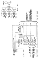
- This register also provides the means to enable these events to trigger the DMA to CPU interrupt for that channel x through the corresponding interrupt enable (IE) bit fields. If a COND bit and its corresponding IE bit are set then that condition is enabled to contribute to the status of the interrupt signal the from the associated DMA Channel to the CPU. If the TCINT bit in the DMA Channel x Control register is set, the logical OR of all enabled conditions forms the DMA_INT x signal. Otherwise, the DMA_INT x remains inactive. This logic is shown in Figure 17. If selected by the interrupt selector, a low to high on that DMA_INT will cause an interrupt condition to be latched by the CPU.
- IE interrupt enable
- the SX COND, WDROP, and RDROP bits in the DMA Channel Secondary Control Register are treated as warning conditions. If these conditions are enabled and active, then they move the DMA channel from the running to the pause state, regardless of the value of the TCINT bit.
- COND bit's associated IE bit may only be cleared by a user write of 0. Otherwise, that COND bit may be automatically cleared as indicated in the following section. A user write of 1 to a COND bit has no effect. Thus, manually forcing one of the conditions cannot be done.
- Table 16 describes each of the conditions in the DMA Channel Secondary Control Register. Depending on the system application, these conditions may represent errors.
- the last frame condition can be used to change the reload register values for auto-initialization. The frame index and element count reload are used every frame. Thus, wait until all but the last frame transfer in a block transfer completes to change these values. Otherwise, the current (rather than the next) block transfer will be affected.
- FRAM E Frame Complete After the last write transfer in each frame is written to memory. A user write of 0 to COND. Two CPU clocks later. LAST Last Frame After all counter adjustments for the next to last frame in a block transfer complete. A user write of 0 to COND. Two CPU clocks later. WDRO P RDRO P Dropped Read/Write Synchron ization A subsequent synchronization event occurs before the last one is cleared. A user write of 0 to COND. BLOC K Block Transfer Complete After the last write transfer in a block transfer is written to memory. A user write of 0 to COND. Two CPU clocks later.
- Figure 18 shows the internal data movement paths of the DMA controller including data buses and internal holding registers.
- Each DMA channel can independently select one of four sources and destinations:
- read and write buses are provided from each interface to the DMA controller.
- the auxiliary channel also has read and write buses. However, as the auxiliary channel provides address generation for the DMA the naming convention of its buses differ. For example, data writes from the auxiliary channel through the DMA are performed through the Auxiliary Write Bus. Similarly, data reads from the auxiliary channel through the DMA are performed through the Auxiliary Read Bus.
- An aspect of the present invention is a 9-deep DMA FIFO 300 holding path that is provided to facilitate bursting to high performances memories including internal program and data memory as well as external synchronous DRAM (SDRAM) or synchronous burst SRAM (SBSRAM).
- SDRAM synchronous DRAM
- SBSRAM synchronous burst SRAM
- read ack's begin. These ack's start removing data from the address FIFO 320 and placing them in the data FIFO 300 along with read data. Thus, the data items are distributed across the three stages. There is counting logic 340 that tracks the number of items stored in each stage.
- the third restriction minimizes "head-of-line" blocking.
- Head-of-line blocking occurs when a DMA request of higher priority waits for a series of lower priority requests to come in before issuing its first request. If a higher priority channel requests control of the DMA controller from a lower priority channel, only the last request of the previous channel has to complete. After that, the higher priority channel completes its requests through its holding registers. The holding registers do not allow as high a throughput through the DMA controller. In the gaps, the lower priority channel begins no more read transfers but is allowed to flush the FIFO by completing its write transfers. As the higher priority channel is not yet in control of the FIFO, there will be gaps in its access where the lower priority channel may drain its transfer from the FIFO. Once the FIFO is clear, if the higher priority channel has not stopped, it gains control of the FIFO.
- the DMA FIFO has two purposes:
- the FIFO allows read transfers to get ahead of write transfers. This feature minimizes penalties for variations in available transfer bandwidth at either end of the element transfer. Thus, the DMA can capitalize on separate windows of opportunity at the read and write portion of the element transfer. If the requesting DMA channel is using the FIFO, the resources are capable of sustaining read or write accesses at the CPU clock cycle rate. However, there may be some latency in performing the first access. The handshaking between the resource and the DMA Controller controls the rate of consecutive requests and the latency of received read transfer data.
- the FIFO cannot be filled.
- data must begin being written out of the FIFO before read requests place data in the last empty FIFO location. From the peripheral handshaking operation, we have determined that a fifo depth of eleven words is required. Thus, at any point in time, the DMA may have up to eleven read transfers in the FIFO queued for their write transfers to complete.
- Decreased Arbitration Latency versus the CPU To capture read data from any pending requests for a particular resource. For example, consider the situation where the DMA is reading data from pipelined external memory such as SDRAM or SBSRAM to internal data memory. Assume the CPU is given higher priority over the DMA channel making requests and that it makes a competing program fetch request of the EMIF. Also, assume that simultaneously, the CPU is accessing all banks of internal memory, blocking out the DMA. In this case, the FIFO allows the pending DMA accesses to complete and the program fetch to proceed. Due to the pipelined request structure of the DMA, at any one point in time the DMA may have up to eleven pending read transfer requests whose data has not yet arrived. Once eleven requests are outstanding, the DMA stops making subsequent read transfer requests.
- Each channel has dedicated internal holding registers. If a DMA channel is transferring data through its holding registers rather than the internal FIFO, read transfers are issued consecutively. Once a read transfer request has been initiated, no subsequent read transfer is started until the read data has arrived within the holding register. Depending whether the DMA controller is in split mode or not additional restrictions can apply:
- the DMA can perform element transfers with single cycle throughput, if it accesses separate resources for the read transfer and write transfer and both these resources have single-cycle throughput.
- An example would be an unsynchronized block transfer from single-cycle external SBSRAM to internal data memory without any competition from either other channels or the CPU.
- the DMA performance can be limited by:
- DMA Action Complete Pins provide a method of feedback to external logic generating an event for each channel (DMAC0-DMAC3). As decided by the DMAC EN bit field in the DMA Channel Secondary Control register, this pin can reflect the status of RSYNC STAT, WSYNC STAT, BLOCK COND, or FRAME COND, or be treated as a high or low general purpose output. If DMAC reflects RSYNC STAT or WSYNC STAT, externally, once a synchronization event has been recognized DMAC will transition from low to high. Once that same event has been serviced (as indicated by the status bit being cleared), DMAC transitions from high to low.
- the DMAC signals are synchronized by CLKOUT2 (1 ⁇ 2 the CPU clock rate).
- the active period of these signals is guaranteed to be a minimum of 2 CLKOUT2 periods wide. Also, even if before synchronization the pulses are only 1 CPU clock period wide, a minimum 2 CLKOUT period active-high pulse occurs the DMAC pin.
- the CPU may be halted on an execute packet boundary for single stepping, benchmarking, profiling, or other debug uses.
- the user may configure whether the DMA pauses during this time or continues running. This function is performed by setting the EMOD bit in the DMA Primary Control register to 0 or 1, respectively. If paused, the STATUS field will reflect the pause state of the channel. The auxiliary channel continues running during an emulation halt.
- European Patent application No. 97310468.0 describes emulation of microprocessor 1 in complete detail, and is incorporated herein by reference.
- the host port interface is a parallel port through which a host processor can have direct access the CPU's memory space.
- the host device is master of the interface, therefore increasing its ease of access.
- the host and CPU can exchange information via internal or external memory.
- the host has direct access to memory mapped peripherals. Connectivity to the CPU's memory space is provided through the DMA controller.
- Dedicated address and data registers not accessible to the CPU connect the HPI to the DMA Auxiliary Channel which in turn connects the HPI to the CPU's memory space.
- HPI and CPU can access the HPI Control Register (HPIC).
- the host can access the host address register (HPIA) and host data register (HPID) as well as the HPIC using the external data and interface control signals ( Figure 19).
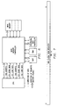
- FIG 19 shows a simplified diagram of host interface to the HPI.
- the HPI provides 32-bit data to the CPU with an economical 16-bit external interface by automatically combining successive 16-bit transfers.
- the DMA Auxiliary Channel accesses the CPU's address space.
- the HPI supports high speed, back-to-back host accesses. In the absence of contention for memory mapped-resources the HPI can transfer one 16-bit value every 4 CPU clocks.
- the DMA auxiliary channel can perform one 32-bit access every 8 CPU clocks.
- the external HPI interface consists of the 16-bit HPI data bus and control signals that configure and control the interface.
- the interface can connect to a variety of host devices with little or no additional logic necessary.
- the 16-bit data bus (HD0--HD15) exchanges information with the host. Because of the 32-bit word structure of the chip architecture, all transfers with a host consist of two consecutive 16-bit halfwords. On host data (HPID) write accesses, the HBE-1:0 byte enables select which bytes in a 32-bit word should be written. HPIA, HPIC accesses, as well as HPID read accesses are performed as 32-bit accesses and the byte enables are not used.
- the dedicated HHWIL pin indicates whether the first or second halfword is being transferred. An internal control register bit determines whether the first or second halfword is placed into the most significant halfword of a word The host must not break the first halfword/second halfword (HHWIL low/high) sequence of an ongoing HPI access.
- the two data strobes (HDS1- and HDS2-), the read/write select (HR/W-), and the address strobe (HAS-) enable the HPI to interface to a variety of industry-standard host devices with little or no additional logic required.
- the HPI can easily interface to hosts with multiplexed or dedicated address/data bus, one data strobe and a read/write strobe, or two separate strobes for read and write.
- the HCNTL1:0 control inputs indicate which HPI register is accessed. Using these inputs, the host can specify an access to the HPIA (which serves as the pointer into CPU's memory space), HPIC, or HPID. These inputs, along with HHWIL, are commonly driven by host address bus bits or a function of these bits. By writing to the HPIC, the host can interrupt the CPU, whereas the CPU can activate HINT- interrupt output to the host.
- the host can access HPID with an optional automatic address increment of HPIA. This feature facilitates reading or writing to sequential word locations.
- auto-increment HPID reads prefetch the data at the auto-incremented access to reduce latency on the subsequent host read request.
- the HPI ready pin HRDY- allows insertion of host wait states. Wait-states may be necessary depending on latency to the point in the memory map accessed via the HPI as well as on the rate of host access. The rate of host access may force not-ready conditions if the host attempts to access the host port before any previous HPID write access or prefetched HPID read access completes. In this case, the HPI simply holds off the host via HRDY-.
- HRDY- provides a convenient way to automatically (no software handshake needed) adjust the host access rate to the rate of data delivery from the DMA auxiliary channel.
- HRDY- pin a HRDY bit in the HPIC is available for use as a software handshake.
- the external HPI interface signals implement a flexible interface to a variety of types of host devices.
- Table 17 lists the HPI pins and their functions. The remainder of this section discusses the pins in detail.
- HPI External Interface Signals Signal Name Signal Type (Input/Output/HI-Z)
- Sig nal Count Host Connection Signal Function HD15:0 I/O/Z 16 Data Bus
- HCNTL1 0 I 2 Address or control lines
- Controls HPI access type Controls HPI access type.
- Halfword identification input HAS- I 1 Address latch enable (ALE) or Address strobe or unused (tied high) ⁇ Differentiates address versus data values on multiplexed address/data host.
- ALE Address latch enable
- Address strobe Address strobe or unused (tied high) ⁇ Differentiates address versus data values on multiplexed address/data host.
- HBE-1:0 I 2 Byte enables Data write byte enables HR/W- I 1 Read/Write strobe, address line, or multiplexed address/ data Read/Write select HCS- I 1 Address or control lines Data strobe inputs.
- HRDY- O 1 Asynchronous ready Ready status of current HPI access
- HD15:0 is a parallel bi-directional 3-state data bus. HD is placed in high-impedance when not performing an HPI read access.
- HCNTL1:0 indicate which internal HPI register is being.
- the states of these two pins select access to the HPI address (HPIA), HPI data (HPID), or HPI control (HPIC) registers.
- HPIA register serves as the pointer into HPI memory, the HPIC contains control and status bits for the transfers, and the HPID contains the actual data transferred. Additionally, the HPID register can be accessed with an optional automatic address increment.
- Table 18 describes the HCNTL0/1 bit functions.
- HHWIL is low for the first halfword and high for the second halfword.
- HBE-1:0 On HPID writes, the value of HBE-1:0 indicates which portions of the 32-bit word must be written. The value of HBE-1:0 is not important on HPIA or HPIC accesses or on HPID reads.
- HBE0- On HPID writes, HBE0- enables the lsbyte in the halfword and HBE1-enables the MSByte in the halfword. Table 19 lists the valid combinations. For byte writes, only a one HBE- in either (but not both) of the halfword accesses may be enabled active-low. For halfword data writes, both the HBE-s must be held active-low in either (but not both) halfword accesses. For word accesses, both HBE- must be held active-low in both halfword accesses. No other combinations are valid.
- HR/W- is the host read write select input. Hosts must drive HR/W high to read HPI and low to write HPI. Hosts without either a read/write select output or a read or write strobe can use an address line for this function.
- HRDY- indicates that the HPI is ready for a transfer to be performed.
- inactive-high HRDY- indicates that the HPI is busy completing the internal portion of current read access of a previous HPID write or HPID read prefetch access.
- HCS- enables HRDY; that is, HRDY is always low when HCS- is low.
- Strobes HCS-, HDS1-, HDS2-
- CS-, HDS1-, HDS2- allow connection to hosts with either:
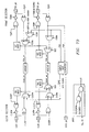
- FIG 20 shows the equivalent circuit of the HCS-, HDS1 -, and H052-inputs.
- HCS-, HDS1, and HDS2- generate an active-low internal HSTRB- signal.
- HSTRB- is only active low when both HCS- is active-low and either (but not both) HDS1 - and HDS2- are active-low.
- the falling edge of HSTRB- (when HAS- is tied inactive-high) samples HCNTL1:0, HHWIL, HR/W-, and HBE-1:0. Therefore, the latest of HDS1-, HDS2-, or HCS- that falls controls the sampling time.
- HCS- serves as the enable input for the HPI and must be low during an access. However, as the HSTRB- signal determines the actual boundaries between accesses, HCS- may stay low between successive accesses as long as both HDS1 - and HDS2- go inactive-high or go active-low.
- Hosts with separate read and write strobes connect those strobes to either HDS1- or HDS2-.
- Hosts with a single data strobe connect it to either HDS1- or HDS2-, connecting the unused pin high. Regardless of HDS connections, HR/W- is still required to determine direction of transfer. Because HDS1-and HDS2- are internally exclusive-NORed, hosts with a high true data strobe can connect this to one of the HDS inputs with the other HDS-input connected low.
- HSTRB- is used for three purposes:
- HCS- gates the HRDY output.
- a not-ready condition is indicated by the HRDY- pin driven inactive-high only if HCS- is active-low.
- HAS- allows HCNTL1:0-, HBE-1:0, HR/W-, and HHWIL to be removed earlier in an access cycle, therefore allowing more time to switch bus states from address to data information.
- This feature facilitates interface to multiplexed address and data type buses.
- an ALE signal is often provided and would normally be the signal connected to HAS-.
- Hosts with a multiplexed address and data bus connect HAS to their ALE pin or equivalent.
- HHWIL, HCNTLO/1, HBE-,and HR/W- are then latched on HAS-'s falling edge.
- HAS- must precede the later of HCS-, HDS1-, or HDS2-.
- Hosts with separate address and data bus can connect HAS high.
- HHWIL, HCNTL0/1, and HR/W are latched by the later of HDS1-, HDS2-, or HCS-falling edge while HAS stays inactive (high).
- Host interrupt output Controlled by the HINT- bit in the HPIC. Driven high when the chip is being reset. This signal is described in more detail later herein.
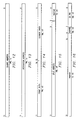
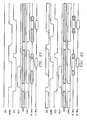
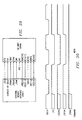
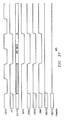
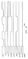
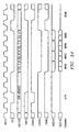
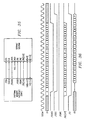
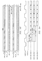
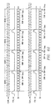
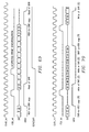
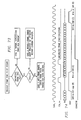
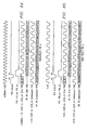
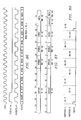
- FIG. 21 and Figure 22 show HPI access timing for the cases when HAS- is not and is used, respectively.
- HAD represents control signals typically driven by host address lines: HCNTL1:0, HR/W-, HHWIL, and HBE-1:0.
- HCNTL1:0 and HR/W should have the same values for both halfword accesses.
- HHWIL is shown separately to indicate that it must be low for the first halfword transfer and high for the second. If HAS is not used (tied high as shown in Figure 21), the falling edge of HSTRB- latches these signals. If HAS is used as shown in Figure 22, the falling edge of HAS- latches these values.
- the falling edge of HAS- must precede the falling edge of HSTRB-.
- data is valid a delay after the falling edge of HSTRB-. If valid data is not already present in the HPID, the data is setup to the rising edge of HRDY- and held until the rising edge of HSTRB. On a write, the host must setup data with respect to the rising edge of HSTRB-.
- HPID contains the data that was read from the HPI memory if the current access is a read, or the data that will be written to HPI memory if the current access is a write. Contains the address in the HPI memory at which the current access occurs. As this address is a 30-bit word address the bottom two bits are unaffected by HPIA writes and are always read as 0.
- HPI Control Register HPIC
- HPIC (See Figure 19A and Table 21) is normally the first register accessed to set configuration bits and initialize the interface.
- the HPIC is organized on the as a 32-bit register with the same high and low halfword contents.
- both halfwords must be identical.
- the low halfword and the high halfword are actually the same storage locations. No storage is allocated for the read only reserved values. Only CPU writes to the lower halfword affect HPIC values and HPI operation.
- the HPIC is normally the first register accessed to set configuration bits and initialize the interface.
- HPIC is organized as a 32-bit register with the same high and low halfword contents.
- the HRDY- pin can indicate to a host that a HPID access has not completed. For example, he current HPID access can be waiting for a previous HPID accesses write to complete or for a previous HPID prefetched read to complete. Also, the current HPID read access can be waiting for is requested data to arrive.
- the HRDY and FETCH bits in the HPIC allow for a software handshake that allows HPI connection in systems where a hardware ready control is not desired. Any prefetched data remains until any HPI register is written or until after the next HPI read, whichever comes first.
- the FETCH and HRDY bits can be used to perform a read transfer as follows:
- the HRDY bit alone can be used for write operations as follows:
- the host and the CPU can interrupt each other using bits in the HPIC register. This subsection presents more information about this process.
- the host can interrupt the CPU by writing to the DSPINT bit in the HPIC.
- the DSPINT bit is tied directly to the internal DSPINT signal.
- the CPU can send an active low interrupt condition on the HINT- signal by writing to the HINT bit in the HPIC.
- the HINT bit is inverted and tied directly to the HINT- pin.
- the host begins HPI accesses by first initializing HPIC, then HPIA, and then writing data to or reading data from HPID. Reading or writing HPID initiates an internal cycle that transfers the desired data between the HPID and the DMA Auxiliary Channel.
- Host access of any HPI register requires two halfword accesses on the HPI bus: the first with HHWIL low, and the second with HHWIL high. Typically, the host does not break the first halfword/second halfword (HHWIL low/high) sequence. If this sequence is broken improperly, data may be lost, and undesired operation may result.
- the first halfword access may have to wait for a previous HPI request to complete. Previous requests include HPID writes and pre-fetched HPID reads. Thus, the HPI will de-assert HRDY- high until the HPI can begin this request. The second halfword access will always have HRDY- active low since all previous accesses have completed by during the first halfword access.
- HPIA Before accessing data, the host must first initialize HPIC, in particular the HWOB bit, and then HPIA (in this order, because HWOB affects the HPIA access). After initializing HWOB, the host can then write to HPIA with the correct halfword alignment.
- HPIA is set to 80001234h. Note that in all these accesses, HRDY bit in the HPIC is set (bit 19 and 3).
- Table 26 shows a read access with auto-increment. After the first halfword access is complete (with the rising edge of the first HSTRB-), the address increments to the next word or 80001238h. Assume that the data at that location is 87654321h. That data is pre-fetched and loaded into HPID. Prefetching begins on the rising edge of HSTRB- on the second halfword read.
- Read Access to HPI With Auto-Increment: HWOB 1 Event Value During Access Value After Access HD HB E-1: 0 HR /W- HC NT L1:0 HR DY- H H W I L HPIC HPIA HPID Host reads 1st halfword Data Not Ready ????
- HPID is transferred as a 32-bit word to the address specified by HPIA with the four related byte-enables.
- the host writes 5566h to the 16 LSBs of location 80001234h, which is already pointed to by HPIA. This location is assumed to start with the value 0.
- the HPI holds of the host until any previous transfers complete by setting HRDY- inactive-high. Also, once the first halfword becomes ready, the second halfword does not encounter any not ready time. If there are no pending writes waiting in HPID, then write accesses normally proceed without a not ready time. Note that the HBE-1:0 is only enabled for the transfer which transfers the 16 LSBs.
- HWOB 1 Event Value During Access Value After Access HD HBE-1:0 HR/W- HCNTL1:0 HRDY- HHWIL HPIC HPIA HPID Location 80001234 Host writes HPID 1st halfword Waiting for Previous 5566 00 0 11 1 0 00010001 80001234 ????5566 00000000 Host wrotes HPID 1 st halfword Ready 5566 00 0 11 0 0 00090009 80001234 ????5566 00000000 Host writes HPIA 2 nd halfword wxyz 11 0 11 0 1 00090009 80001234 wxyz5566 00005566
- HWOB 1 Event Value During Access Value After Access HD HBE-1:0 HR/W- HCNTL1:0 HRDY- HHWIL HPIC HPIA HPID Location 80001234 Location 80001238 Host writes HPID 1st halfword Waiting for Previous 5566 00 0 10 1 0 00010001 80001234 ????5566 00000000 00000000 Host wrotes HPID 1 st halfword Ready 5566 00 0 10 0 0 00090009 80001234 ????5566 0000000000000000 Host writes HPIA 2 nd halfword wxyz 11 0 10 0 1 00090009 80001234 wxyz5566 00005566 00000000 Host writes HPID 1 st halfword Waiting for Previous nopq 11 0 10 1 0 00010001 80001234 wxyznopq 00005566 00000000 Host writes HPID 1 st
- every transfer must consist of two halfword accesses.
- the user may perform single-halfword accesses. These can be useful in several cases:
- Write accesses are triggered by the second halfword access (HHWIL is high).
- HHWIL is high.
- the HPI cannot be used while the chip is in reset.
- certain boot modes may allow the host to write the CPU's memory space (including configuring EMIF configuration registers to configure external memory before accessing it).
- the device is not in reset, the CPU itself is in reset until the boot completes. Refer to the bootload section later herein for full details.
- the External Memory Interface supports a glueless interface to several external devices including:
- FIG. 23 A block diagram of the EMIF is shown in Figure 23.
- Table 32 describes the EMIF signals.
- EA(21 :2) O/Z External Address output. Drives bits 21-2 of the byte address. /CEO O/Z External /CEO Chip Select. Active low chip select for CE space 0.
- Active low write strobe for asynchronous memory interface /ARE O/Z Read Strobe. Active low read strobe for asynchronous memory interface. /SSAD S O/Z Address Strobe. Active low address strobe/enable for SBSRAM interface. /SSOE O/Z Output Enable. Output buffer enable for SBSRAM interface. /SSWE O/Z Write Enable. Active low write enable for SBSRAM interface. SSCLK O/Z Clock. SBSRAM interface clock; equivalent to CLKOUT1 or CLKOUT2 as selected by the user. /SDRA S O/Z Row Address Strobe. Active low /RAS for SDRAM memory interface. /SDCA S O/Z Column Address Strobe. Active low /CAS for SDRAM memory interface.
- /SDWE O/Z Write Enable Active low /W for SDRAM memory interface.
- /HOLD I Hold Active low external bus hold (tristate) request.
- /HOLD A O Hold Acknowledge Active low external bus hold acknowledge.
- a hardware reset using the /RESET pin on the device forces all register values to their reset state. During reset, all outputs are driven to their inactive levels, with the exception of the clock outputs (SDCLK, SSCLK, CLKOUT1 and CLKOUT2), which continue to be driven such that external logic which is using these signals can be synchronized.
- EMIF Memory Mapped Registers Byte Address Name 0x01800000 EMIF Global Control 0x01800004 EMIF CE1 Space Control 0x01800008 EMIF CE0 Space Control 0x0180000C Reserved 0x01800010 EMIF CE2 Space Control 0x01800014 EMIF CE3 Space Control 0x01800018 EMIF SDRAM Control 0x0180001C EMIF SDRAM Refresh Period
- the EMIF Global Control Register ( Figure 24 and Table 34) configures parameters common to all the CE spaces.
- the four CE Space Control Registers correspond to the four CE spaces supported by the EMIF.
- the MTYPE field identifies the memory type for the corresponding CE space. If MTYPE selects SDRAM or SBSRAM, the remaining fields in the register do not apply. If an asynchronous type is selected (ROM or Asynchronous), the remaining fields specify the shaping of the address and control signals for access to that space. Modification of a CE Space Control Register does not occur until that CE space is inactive.
- the number of CLKOUT1 cycles between reads and writes or between accesses to different CE spaces Measured from when /OE rises.
- One turn-around cycle is inserted between a write followed by a read.
- One turn-around cycle is inserted between consecutive accesses to two different CE spaces from the same requester.
- TA 00b, 1 turn-around cycle.
- TA 01b, 2 turn-around cycles.
- TA 10b, 3 turn-around cycles.
- TA 11b, 4 turn-around cycles.
- MTYPE Memory Type MTYPE Memory Type.
- the SDRAM Control Register controls SDRAM parameters for all CE spaces which specify an SDRAM memory type in the MTYPE field of its associated CE Space Control Register ( Figure 25). Since the SDRAM Control Register controls all SDRAM spaces, each space must contain SDRAM with the same refresh and page characteristics.
- NIT 0, no effect.
- NIT 1, initialize SDRAM in each CE space configured for SDRAM.
- RFEN 0, SDRAM refresh disabled.
- RFEN 1, SDRAM refresh enabled.
- the SDRAM refresh period register ( Figure 27 and Table 37) controls the refresh PERIOD for SDRAM in terms of CLKOUT2 cycles (1 ⁇ 2x the CPU clock rate).
- the refresh period can send an interrupt to the CPU.
- this counter may be used as a general purpose timer if SDRAM is not used by the system.
- the COUNTER value can be read by the CPU. When the counter reaches zero, it is automatically reloaded with the PERIOD, and an interrupt is sent to the CPU.
- the EMIF supports 16 Mbit, 2 bank and 64Mbit, 4 bank SDRAM offering system designers an interface to high speed and high density memory.
- the following sections describe the EMIF SDRAM interface.
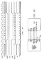
- the EMIF supports the SDRAM commands shown in Table 38. 16M bit and 64 Mbit SDRAM interfaces are shown in Figure 28 and Figure 29.
- Table 40 describes the pin connection and related signals specific to SDRAM operation.
- Table 39 shows all of the possible SDRAM configurations available via the EMIF.
- DQM[3:0] Data / output mask.
- DQM is an input/output buffer control signal. It disables writes and tri-states outputs during reads when high. DQM has a 2 CLK latency on reads and a 0 CLK latency on writes. DQM pins serve essentially as byte strobes and are connected to /BE[3:0] outputs.
- /CS must be active-low for a command to be clocked into the SDRAM. /CS does not affect data input or output once a write or read has begun.
- - CKE CKE clock enable Tied active high when interface to EMIF to always enable clocking.
- CLKOUT2 CLK SDRAM clock input. Runs at 1 ⁇ 2 the CPU clock rate.
- the EMIF performs the necessary functions to initialize SDRAM if any of the CE spaces are configured for SDRAM.
- An SDRAM initialization is requested by a write of 1 to the INIT in the EMIF SDRAM Control Register.
- the actual sequence of events of an initialization is as follows:
- the DCAB cycle is performed immediately after reset, provided the /HOLD input is not active (a host request). If /HOLD is active, the DCAB command will not be performed until the hold condition is removed. The external requester should not attempt to access any SDRAM banks in this case, unless it performs SDRAM initialization and control itself.
- the EMIF SDRAM controller monitors the active row of SDRAM so that row boundaries are not crossed during the course of an access. To accomplish this monitoring, the EMIF stores the address of the open page, and performs compares against that address for subsequent accesses to the SDRAM bank. This storage and comparison is performed independently for each CE space.
- the EMIF performs a DCAB command and starts a new row access. Also, a change in direction of an access (read to write or write to read) causes a page miss. Note that simply ending the current access is not a condition which forces the active SDRAM row to be closed. The EMIF speculatively leaves the active row open until it becomes necessary to close it. This feature decreases the deactivate-reactivate overhead and allows the interface to fully capitalize on address locality of memory accesses.
- the RFEN bit in the SDRAM Control Register selects the SDRAM refresh mode of the EMIF.
- a value of 0 in the RFEN field disables all EMIF refreshes, the user must insure that refreshes are implemented in an external device.
- a value of 1 in the RFEN field enables the EMIF to perform refreshes of SDRAM as described below.
- REFR Refresh commands
- REFR enable all /CE signals for all CE spaces selected to use SDRAM with the MTYPE field of the CE Space Control Register ( Figure 25).
- REFR is automatically preceded by a DCAB command. This ensures all CE spaces selected with SDRAM are deactivated.
- the EMIF begins performing "trickle" refreshes, at a rate defined by the PERIOD value in the EMIF SDRAM Control register provided no other SDRAM access is pending.
- the SDRAM interface monitors the number of refresh requests posted to it and performs them.
- a small 2 bit counter monitors the backlog of refresh requests. The counter increments once for each refresh request and decrements once for each refresh cycle performed. The counter will saturates at the value of 11, and also at 00. At reset, the counter is automatically set to 11, to ensure that several refreshes occur before accesses begin.
- the EMIF SDRAM controller prioritizes SDRAM refresh requests with other data access requests posted to it from the EMIF requesters. The following rules are followed:
- the EMIF SDRAM interface performs CAS-before-RAS refresh cycles for SDRAM. Some SDRAM manufacturers call this auto-refresh. Prior to a REFR command, a DCAB command is performed to all CE spaces specifying SDRAM to ensure that all active banks are closed. Page information is always invalid before and after a REFR command; thus a refresh cycle always forces a page miss. Note that a deactivate cycle is required prior to the refresh command.
- the EMIF automatically performs a DCAB command followed by a MRS command whenever the INIT field in the EMIF SDRAM Control Register is set.
- INIT can be set by device reset, or by a user write.
- MRS commands are performed to all CE spaces configured as SDRAM through the MTYPE field to hold.
- the INIT bit clears itself to prevent multiple MRS cycles. Following an should return it to its original value before returning control of the bus to the EMIF.
- the user could poll the HOLD and HOLDA bits in the EMIF Global control register and upon detecting completion of an external hold re-initialize the EMIF by setting the INIT bit in the EMIF SDRAM Control Register.
- the EMIF always uses a Mode Register value of 0x0030 during a MRS command.
- Table 41 shows the mapping between mode register bits, EMIF pins, and the mode register value.
- Table 42 shows the SDRAM configuration selected by this mode register value.
- Mode Register Value Mode Register Bit 13 12 1 1 10 9 8 7 6 5 4 3 2 1 0 EMIF Pins EA 15 EA 14 EA13 SDA10 EA11 EA10 EA9 EA8 EA7 EA6 EA5 EA4 EA3 EA2 Field Reserved Write Burst Length Reserved Read Latency S/I Burst Length Value 0 0 0 0 0 0 0 1 1 0 0 0 0 0 Implied SDRAM Configuration by MRS Value Field Selection Write Burst Length 1 Read Latency 3 Serial/Interlea ve Burst Type Serial Burst Length 1
- Table 43 shows the translation between bits of the byte address and how they appear on the EA pins for row and column addresses. SDRAMs use the address inputs for control as well as address. W ith this consideration, the following items clarify the figure:
- the selected bank is activated with the row address during the ACTV command.
- the EMIF uses a CAS latency of 3 and a burst length of 1.
- the 3 cycle latency causes data to appear 3 cycles after the corresponding column address.
- a DCAB cycle is performed to deactivate the bank.
- An idle cycle is inserted between the final read command and the DCAB command to meet SDRAM timing requirements. Note that the transfer of data completes during and past the DCAB command. If no new access is pending, the DCAB command is not performed until such time that the page information becomes invalid.
- the values on EA[13:11] during column accesses and the DCAB command are the values latched during the ACTV command.
- the EMIF interfaces directly to industry standard synchronous burst SRAMs.
- This memory interface allows a high speed memory interface without some of the limitations of by SDRAM.
- SBSRAM are SRAM devices, random accesses in the same direction may occur in a single cycle.
- the SBSRAM interface may run at either the CPU clock speed or at 1 ⁇ 2 of this rate. The selection is made based on the setting of the SSCRT bit in the EMIF Global Control Register.
- the four SBSRAM control pins of Table 45 are latched by the SBSRAM on the rising SSCLK edge to determine the current operation. These signals are only valid if the chip select line for the SBSRAM is low.
- the /ADV signal is used to allow the SBSRAM device to generate addresses internally for interfacing to controllers which cannot provide addresses quickly enough.
- the EMIF does not need to use this signal because it can generate the address at the required rate.
- SBSRAMs are latent by their architecture, meaning that read data follows address and control information. Consequently, the EMIF inserts cycles between read and write commands to ensure that no conflict exists on the ED[31:0] bus. The EMIF keeps this turn-around penalty to a minimum.
- the initial 2-cycle penalty is present when changing directions on the bus. In general, the rule is this; the first access of a burst sequence will incur a 2 cycle startup penalty.
- Figure 36 shows a 16 word read of an SBSRAM. Every access strobes a new address into the SBSRAM, indicated by the /SSADS strobe low. The first access requires an initial startup penalty of 2 cycles; thereafter all accesses occur in a single SSCLK cycle.
- Figure 37 shows a 6 word write of an SBSRAM. Every access strobes a new address into the SBSRAM. The first access requires an initial startup penalty of 2 cycles; thereafter all access can occur in a single SSCLK cycle.
- the asynchronous interface offers users configurable memory cycle types, used to interface to a variety of memory and peripheral types; including, SRAM, EPROM, FLASH, as well as FPGA and ASIC designs.
- Table 46 lists the asynchronous interface pins.
- Figure 38 shows an interface to standard SRAM.
- Figure 39 shows an interface to FIFOs.
- Figure 40, Figure 41, and Figure 42 show interfaces to 8-, 16-, and 32-bit ROM.
- ROM may be interfaced at any of the CE spaces, it is often used at CE1 space because that space may be configured for widths of less than 32 bits.
- EMIF Asynchronous Interface Pins
- EMIF Signal Function /AOE Output Enable - active low during the entire period of a read access.
- /AWE Write Enable - active low during a write transfer strobe period.
- /ARDY Ready input used to insert wait states into the memory cycle.
- the EMIF supports 8- and 16-bit wide ROMs access mode as selected by the MTYPE field in the EMIF CE Space Control Register. In reading data from these narrow width memory spaces, the EMIF packs multiple reads into one 32-bit wide value. This mode is primarily intended for word access to 8-bit and 16-bit ROM devices. Thus, the following restrictions apply:
- 8-bit ROM mode the address is left shifted by 2 to create a byte address on EA to access byte wide ROM.
- the bytes are fetched in the following address order: 4N, 4N+1, 4N+2, 4N+3.
- Bytes are packed into the 32-bit word in the following little endian order from MSByte to LSByte: 4N+3, 4N+2, 4N+1, 4N.
- the address is left shifted by 1 to create a half-word address on EA to access 16-bit wide ROM.
- the halfwords are fetched in the following address order: 4N, 4N+2.
- Halfwords are packed into the 32-bit word in the following little endian order from MSHalfword to LSHalfword: 4N+2, 4N.
- the EMIF allows a high degree of programmability for shaping asynchronous accesses.
- the programmable parameters that allow this are:
- Figure 43 illustrates three asynchronous reads. The first is a CEO read with setup/strobe/hold set to 2/4/1. The second is the same but with additional strobe width due to an external inactive ready. The third is a CE1 read with setup/strobe/hold set to 4/5/3.
- An asynchronous read proceeds as follows:
- the first access in Figure 43 illustrates an asynchronous write with a setup/strobe/hold of 3/6/3.
- An asynchronous write proceeds as follows.
- Figure 43 illustrates usage of the programmable turn-around parameter. To prevent bus contention the EMIF inserts programmable turn-around cycles in two situations:
- the second CEO space read in Figure 43 illustrates read operation.
- /ARDY Because of the delay in the effects of /ARDY, one must be careful when setup and strobe times are very small. For example, with strobe periods of 1, the /ARDY is sampled two cycle before the end of the setup period. In this case, if the setup period is 2, the /ARDY is sampled on the same edge that begins the access.
- the EMIF responds to hold requests for the external bus.
- the hold handshake allows an external device and the EMIF to share the external bus.
- the handshake mechanism uses two signals:
- Table 48 illustrates the priority scheme that the EMIF will use in the case of multiple pending requests.
- the priority scheme may change if the DMA channel that is issuing a request through the DMA controller is of high priority. This mode is set in the DMA by setting the PRI bit in the DMA Channel Primary Control Register.
- a requester (note in this instance the refresh controller is considered a requester also) is prioritized and chosen, no new requests will be recognized until either the chosen requester stops making requests or a subsequent higher priority request occurs. In this case, all issued requests of the previous requester will be allowed to complete while the new requester starts making its requests.
- the EMIF allows disabling (holding high) CLKOUT2, CLKOUT1, SSCLK, and SDCLK. This feature is performed via the CLK2EN, CLK1EN, SSCEN, and SDCEN bits in the EMIF SDRAM control register.
- the EMIF continues operating during emulation halts. Emulator accesses through the EMIF can have the effect of changing EMIF state and forcing startup penalties once the halt is stopped.
- the device For proper device initialization, the device provides a variety of boot configurations. These configurations determine what actions the microprocessor 1 performs after device reset to prepare for initialization. These boot configurations, which are set by external input pins, determine:
- the external device reset 76 is an active low RESET-signal. While RESET- is active low the device is held in reset. During this period the device is initialized to the prescribed reset state. All tri-stateable outputs are tristated. All other outputs are returned to the state as described in the associated chapter. To allow reset is latched with the device CLKIN as well as the CPU clock. Thus, reset has minimum low time in terms of CLKIN as well as CPU clock (CLKOUT1) cycles. The precise timing requirements for device reset are described in the data sheet. The rising edge of RESET- starts the processor running with the prescribed boot configuration.
- BOOTMODE[4:0] determines the boot configuration for the part.
- the value of BOOTMODE[4:0] is latched with the rising edge of RESET-. These pins must be valid with the proper setup and hold to this edge. Refer to the data sheet for specific timing requirements. This boot configuration determines (Table 49):
- MAP 0 and MAP 1 There are two memory maps, MAP 0 and MAP 1 (Table 50). They differ in that MAP 0 has external memory mapped at address 0 and MAP 1 has internal memory mapped at address 0. Note the spaces allocated for internal peripherals represent space reserved for that purpose. The entire memory space reserved may not be populated. Refer to the appropriate discussion for the peripherals and internal herein.
- the boot configuration determines the type of memory located at the reset address for processor operation, address 0.
- the BOOTMODE pins select MAP 1, this memory is internal.
- the device mode is in MAP 0, the memory is external.
- BOOTMODE also determines the type of memory at the reset address. Effectively, these options provide alternative reset values to the appropriate EMIF control registers.
- the boot process also is determined by the BOOTMODE pins as shown in Table 50. Three types of boot processes are available:
- the Multi-Channel Serial Port is an improvement on a known serial port interface found on the TMS320C2x, and 'C5x, Digital Signal Processor devices available from Texas Instruments Incorporated. A detailed description of this serial port is provided in U.S. Patent No. (application TI-19942) which is incorporated herein by reference. Like its predecessors the MCSP provides the following features:
- MCSP 120 consists of a data path and control path as shown in Figure 44. Seven external pins 121a-121g listed in Table 51 connect the control and data paths to external devices.
- the data is communicated to devices interfacing to the MCSP via the Data Transmit (DX) pin for transmit and the Data Receive (DR) pin for receive.
- Control information in the form of clocking and frame synchronization is communicated via CLKX, CLKR, FSX, and FSR.
- Processor 1 communicates to the MCSP via 32-bit wide control registers accessible via the internal peripheral bus 110.
- the CPU 10 or DMA 100/101 reads the received data from the Data Receive Register (DRR) and writes the data to be transmitted to the Data Transmit Register (DXR).
- Data written to the DXR is shifted out to DX via the Transmit Shift Register (XSR).
- receive data on the DR pin is shifted into RSR and copied into RBR.
- RBR is then copied to DRR which can be read by the CPU or DMA.
- the remaining registers which are accessible to CPU 10, configure the control mechanism of the MCSP. These registers are listed in Table 52.
- the control block consists of internal clock generation, frame synchronization signal generation, and their control, and multi-channel selection. This control block sends notification of important events to the CPU and DMA via four signals shown in Table 53.
- the serial port is configured via the 32-bit Serial Port Control Register (SPCR) and Pin Control Register as shown in Figure 45 and Figure 46, respectively.
- SPCR Serial Port Control Register
- PCR contains MCSP status information and contains bits that can be configured for desired operation. The operation of each bit-field will be discussed in later sections.
- Table 54 and Table 55 describe each bit field of the SPCR and PCR, respectively.
- DR STAT DR pin status Reflects value on DR pin.
- CLKS_ STAT CLKS pin status Reflects value driven on to CLKS pin when selected as a general purpose output.
- DX_STAT DX pin status Reflects value driven on to DX pin when selected as a general purpose output.
- DR_STAT DR pin status Reflects value on DR pin when selected as a general purpose input.
- Receive and Transmit Control Registers shown in Figure 47 and Figure 48 configure various parameters of receive and transmit operation respectively. The operation of each bit-field will be discussed in later sections. Table 56 describes each bit field of RCR and XCR.
- Modes other than 00b are only enabled when the appropriate (R/X)WDLEN is 000b, indicating 8-bit data.
- (R/X)COMPAND 00b, no companding, data transfer starts with MSB first.
- (R/X)COMPAND 01b, no companding, 8-bit data, transfer starts with LSB first.
- (R/X)COMPAND 10b, compand using ⁇ -law for receive/transmit data.
- (R/X)COMPAND 11b, compand using A-law for receive/transmit data.
- RFIG XFIG Receive/Transmit Frame Ignore (R/X)FIG 0, Receive/Transmit Frame synchronization pulses after the first restarts the transfer.
- the receive operation is triple-buffered and transmit operation is double buffered.
- Receive data arrives on DR and is shifted into the RSR. Once a full word (8-, 12-, 16-, 20-, 24-, or 32-bit) is received, the RSR is always copied to the Receive Buffer Register, RBR. RBR is then copied to DRR unless DRR is not read by the CPU or DMA.
- Transmit data is written by the CPU or DMA to the DXR. If there is no data in the XSR, the value in the DXR is copied to the XSR. Otherwise, the DXR is copied to the XSR after the last bit of data in the DXR has been shifted out on DX. After transmit frame synchronization, the XSR begins shifting out the transmit data on DX.
- the serial port initialization procedure includes the following steps:
- the transmitter and receiver may be placed in or taken out of reset individually by only modifying the desired bit.
- the necessary duration of the active-low period of XRST- or RRST- is at least two bit clocks (CLKR/CLKX) wide.
- the Ready Status is indicated by RRDY and XRDY.
- RRDY and XRDY indicate the ready status of the MCSP receiver and transmitter, respectively.
- writes and reads of the serial port may be synchronized by polling RRDY and XRDY, or by using the events to DMA (REVT and XEVT) or interrupts to CPU (RINT and XINT) that they generate. Note that reading the DRR and writing to DXR affects RRDY and XRDY.
- XRDY When the transmitter transitions from reset to non-reset (XRST- transitions from 0 to 1), the XRDY also transitions from 0 to 1 indicating that the DXR is ready for new data.
- XRDY is cleared to 0.
- XRDY transitions again from 0 to 1.
- the CPU or DMA can write to DXR although XSR has not been shifted out on DX as yet.
- XRDY directly drives the transmit synchronization event to the DMA (XEVT).
- CPU Interrupts are requested by (R/X)INT.
- the receive interrupt (RINT) and transmit interrupt (XINT) signals the CPU of changes to the serial port status.
- RINT receive interrupt
- XINT transmit interrupt
- Figure 49 shows typical operation of the MCSP clock and frame sync signals.
- Serial clocks CLKR, and CLKX define the boundaries between bits for receive and transmit respectively.
- frame sync signals FSR and FSX define the beginning of a serial word.
- the MCSP allows configuration of various parameters for data frame synchronization. This can be done independently for receive and transmit which includes the following options:
- Receive and transmit frame sync pulses can be generated either internally by the sample rate generator (described later) or driven by an external source. This can be achieved by programming the mode bit, FS(R/X)M, in the PCR. FSR is also affected by the GSYNC bit in the SRGR (described later). Similarly, receive and transmit clocks can be selected to be inputs or outputs by programming the mode bit, CLK(R/X)M, in the PCR.
- FSR and FSX are outputs, implying that they are driven by the sample rate generator, they are generated (transition to their active state) on the rising edge of internal clock, CLK(R/X)_int. Similarly data on DX pin is output on the rising edge of CLKX_int.
- the configuration is so that the receiver can reliably sample data that is clocked with a rising edge clock (by the transmitter).
- FIG. 50 shows how data clocked by an external serial device using a rising edge may be sampled by the MCSP receiver with the falling edge of the same clock.
- Frame Synchronization Phases will now be described.
- Frame synchronization is used to indicate the beginning of a transfer on the MCSP.
- the data stream following frame synchronization may have two phases, phase 1 and phase 2.
- the number of phases in a data stream can be selected by the phase bit, (R/X)PHASE, in the RCR and XCR.
- the number of words per frame and bits per word can be independently selected for each phase via (R/X)FRLEN(1/2) and (R/X)WDLEN(1/2) respectively.
- Figure 51 shows an example of a frame where the first phase consists of 2 words of 12 bits each followed by a second phase of 3 words of 8 bits each. Note that the entire bit stream in the frame is contiguous. There are no gaps either between words or between phases.
- Table 58 shows the bit-fields in the receive/transmit control register (RCR/XCR) that control the number of words/frame and bits/word for each phase for both the receiver and transmitter.
- the maximum number of words per frame is 128, and the number of bits per word can be 8-, 12-, 16-, 20-, 24-, or 32-bits.
- RCR/XCR Bit-fields Controlling Words/Frame and Bits/Word Serial Port MCSP0/1 Frame Phase
- Frame Length (R/X)FRLEN(1/2), will now be described, with reference to Table 59.
- Frame length can be defined as the number of serial words (8-, 12-, 16-, 20-, 24-, or 32-bit) transferred per frame. It corresponds to the number of words or logical time slots or channels per frame synchronization signal.
- the example in Figure 52 can also be treated as a data stream of a single phase frame consisting of one 32-bit data word as shown in Figure 53.
- Figure 53 In this case:
- one 32-bit data word is transferred to and from the MCSP by the CPU or DMA.
- DRR one read of DRR and one write of DXR is necessary for each frame. This results in only one-fourth the number of transfers compared to the previous case. This manipulation reduces the percentage of bus time required for serial port data movement.
- RDATDLY Data Delay
- XDATDLY Data Delay
- the start of a frame is defined by the first clock cycle in which frame synchronization is found to be active.
- the beginning of actual data reception or transmission with respect to the start of the frame can be delayed if required. This delay is called data delay.
- RDATDLY and XDATDLY specify the data delay for reception and transmission, respectively.
- 1-bit delay is selected as data often follows a one-cycle active frame sync pulse.
- frame sync pulse is detected or sampled with respect to an edge of serial clock CLK(R/X)_int (described earlier).
- CLK(R/X)_int an edge of serial clock CLK(R/X)_int
- data may be received or transmitted.
- the data must be ready for reception and/or transmission on the same serial clock cycle.
- receive data is sampled on the first falling edge of CLKR_int where an active high FSR_int is detected.
- data transmission must begin on the rising edge of CLKX_int clock that generated the frame synchronization. Therefore, the first data bit is assumed to be present in the XSR and thus DX.
- the transmitter then asynchronously detects the frame synchronization, FSX_int, going active high, and immediately starts driving the first bit to be transmitted on the DX pin.
- Another common mode is a data delay of two.
- This configuration allows the serial port to interface to different types of T1 framing devices where the data stream is preceded by a framing bit.
- the serial port essentially discards the framing bit from the data stream as shown in Figure 55.
- the serial port In transmission, by delaying the first transfer bit, the serial port essentially inserts a blank period (high impedance period) where framing bit should be.
- the framing device inserts its own framing bit or that the framing bit is generated by another device.
- FIG. 56 shows an example of the Audio Codec '97 (AC97) standard which uses the dual phase frame feature.
- the first phase consists of a single 16-bit word.
- the second phase consists of 12 20-bit words.
- the phases are configured as follows:
- Figure 56 shows the timing of AC97 near frame synchronization.
- the frame sync pulse itself overlaps the first word.
- the inactive to active transition of the frame synchronization signal actually indicates frame synchronization. For this reason, frame synchronization may be high an arbitrary number of bit clocks. Only after the frame synchronization is recognized to have gone inactive and then active again is the next frame synchronization recognized.
- MCSP Standard Operation Mode will now be described. Depending on the mode of operation, there can be periods of serial port inactivity between packets or transfers. In this case, the receive and transmit frame synchronization pulse occurs for every serial word transfer.
- Figure 58 shows an example of a single phase data frame comprising one 8-bit word. Since the transfer is configured for one data bit delay, the data on the DX and DR pins are available one bit clock after FS(R/X) goes active. This figure as well as all others in this section make the following assumptions:
- Figure 59 shows an example of serial reception.
- FSR_int receive frame synchronization
- the data on the DR pin is then shifted into the receive shift register (RSR) after the appropriate data delay as set by RDATDLY.
- the contents of RSR is then shifted to RBR.
- RRDY is activated on every RBR-to-DRR copy to indicate that the receive data register (DRR) is ready with the data to be read by the CPU or DMA.
- RRDY is deactivated when the DRR is read by the CPU or DMA.
- Figure 60 shows an example of serial transmission.
- the value in the transmit shift register, XSR is shifted out and driven on the DX pin after the appropriate data delay as set by XDATDLY.
- XRDY is activated on every DXR-to-XSR copy indicating that the data transmit register (DXR) is written with the next data to be transmitted.
- XRDY is deactivated when the DXR is written by the CPU or DMA.
- Figure 61 shows the MCSP operating at maximum packet frequency.
- the total number of words in a frame, whether single phase or dual phase, may be called the serial transfer packet.
- the data bits in consecutive packets are transmitted contiguously with no inactivity between bits. If there is a one-bit data delay as shown, the frame synchronization pulse overlaps the last bit transmitted in the previous packet.
- the MCSP can be configured to ignore transmit and receive frame synchronization pulses.
- the (R/X)FIG bit in the (R/X)CR can be programmed to zero and not ignore frame sync pulses, or, be set to one and ignore frame sync pulses. This way the user can use (R/X)FIG bit to either pack data or ignore unexpected frame sync pulses. Data packing is explained in the following paragraph; and MCSP operation on unexpected frame sync pulses in the next paragraph.
- reception the reception of B is aborted (B is lost), and a new data word (C in this example) is received after the appropriate data delay.
- This condition is a receive synchronization error and thus sets the RSYNCERR field.
- transmission the transmission of B is aborted, and the same data (B) is retransmitted after the appropriate data delay.
- This condition is a transmit synchronization error and thus sets the XSYNCERR field. Synchronization errors are discussed later.
- the transfer of word B is not affected by an unexpected frame synchronization.
- RFULL 1 in the SPCR indicates that the receiver has experienced overrun.
- any new data input on DR pin will still be shifted into RSR.
- Figure 66 shows a receive overrun condition. Because serial word A is not read before the completion of the reception of serial word B, B is never transferred to the DRR. Thus, at the end of reception of B, RFULL is set. When the DRR is finally read, the value A is still in the DRR. Because the read of the DRR occurs after the serial word C has started transfer, C is never shifted into the RSR.
- Figure 67 shows the case where RFULL is set, but the overrun condition is averted by reading the contents of DRR before the next serial word. This ensures an RBR-to-DRR copy of data B occurs before the next serial word is transferred from RSR to RBR.
- Figure 70 depicts what happens if the data in DXR is overwritten before being transmitted. Initially, the programmer loaded the DXR with data C. A subsequent write to the DXR overwrites C with D before it is copied to the XSR. Thus, C is never transmitted on DX.
- the DMA can avoid overwriting by write synchronizing data transfers with XEVT.
- XEMPTY- 0
- the transmitter halts and places DX in high-impedance until the next frame synchronization.
- Figure 71 depicts a transmit under-flow condition. After B is transmitted, the programmer fails to reload the DXR before the subsequent frame synchronization. Thus, B is again transmitted on DX.
- Figure 72 shows the case of writing to DXR just before a transmit under-flow condition that would otherwise occur. After B is transmitted, C is written to DXR before the next transmit frame sync pulse occurs so that C is successfully transmitted on DX, thus averting a transmit empty condition.
- Figure 74 shows the case for normal operation of the serial port with inter-packet intervals.
- XSYNCERR bit in the SPCR is set.
- XSYNCERR can only be cleared by transmitter reset or by the user writing a 0 to this bit in the SPCR.
- the XSYNCERR bit in the SPCR is a read/write bit. Therefore, writing a 1 to it sets the error condition. Typically, writing a 0 is expected.
- RJUST Receive Data Justification and Sign-Extension, RJUST, will now be described.
- RJUST in the SPCR selects whether data in the RBR is right or left justified (with respect to the MSB) in the DRR. If right-justification is selected RJUST further selects whether the data is sign-extended or zero-filled.
- Table 61 shows the effect various modes of RJUST have on an example 12-bit receive data value 0xABC.
- Companding (COMpress and exPAND) hardware allows compression and expansion of data in either ⁇ -law or A-law format.
- the companding standard employed in the United States and Japan is ⁇ -law.
- the European companding standard is referred as A-law.
- the specification for ⁇ -law and A-law log PCM is part of the CCITT G.711 recommendation.
- A-law and ⁇ -law allows 13-bits and 14-bits of dynamic range, respectively. Any values outside this range will be set to the most positive or most negative value.
- the ⁇ -law and A-law formats encode this data into 8-bit code words.
- the appropriate (R/X)WDLEN(1/2) must be set to 0, indicating 8-bit wide serial data stream. If either phase of the frame does not have 8-bit word length, then companding is automatically disabled for that portion (transmit or receive) and phase.
- transmit data is encoded according to specified companding law, and receive data is decoded to 2's complement format.
- Companding is enabled and the desired format selected by appropriately setting (R/X)COMPAND in the (R/X)CR as shown in Table 56. Compression occurs during the process of copying data from the DXR-to-XSR and from the RBR-to-DRR as shown in Figure 75.
- the 8-bit compressed data in RBR is expanded to a left-justified 16-bit data, LAW16. This can be further justified to a 32-bit data by programming the RJUST field in the SPCR as shown in Table 62.
- the companding hardware can compand internal data. This can be used to:
- Figure 77 shows two methods by which the MCSP can compand internal data.
- the MCSP has several means of selecting clocking and framing for both the receiver and transmitter. Clocking and framing can be sent to both portions by the sample rate generator. Both portions can select external clocking and/or framing independently.
- Figure 38 shows a block diagram of the clock and frame selection circuitry. The features enabled by this logic are explained in the following paragraphs.
- the sample rate generator is composed of a three stage clock divider that allows programmable data clocks (CLKG) and framing signals (FSG) as shown in Figure 79.
- CLKG and FSG are MCSP internal signals that can be programmed to drive receive and/or transmit clocking (CLKR/X) and framing (FSR/X).
- CLKR/X receive and/or transmit clocking
- FSR/X framing
- the sample rate generator can be programmed to be driven by an internal clock source or an internal clock derived from an external clock source.
- the three stages compute:
- a frame pulse detection and clock synchronization module allows synchronization of the clock divide down with an incoming frame pulse.
- Sample Rate Generator Register shown in Figure 80 and Table 63 controls the operation of various features of the sample rate generator. The following sections describe how its operation can be configured using the SRGR bit-fields.
- frame period FPER
- FPER frame period
- CLKSM 1 Sample rate generator clock derived from CPU clock.
- FSGM 0, Transmit frame sync signal (FSX) due to DXR-to-XSR copy.
- FPER Frame Period This determines when the next frame sync signal should become active.
- FWID Frame Width Determines the width of the frame sync pulse, FSG, during its active period.
- CLKGDV Sample rate generator clock divider This value is used as the divide-down number to generate the required sample rate generator clock frequency.
- the CLK GDV field determines the sample rate generator data bit clock rate.
- the first divider stage generates the serial data bit clock from the input clock. This divider stage utilizes a counter that is pre-loaded by CLKGDV which contains the divide ratio value. The output of this stage is the data bit clock which is output on sample rate generator output, CLKG, and serves as the input for the second and third divider stages.
- CLKG has a frequency equal to 1/(CLKGDV+1) of sample rate generator input clock.
- sample generator input clock frequency is divided by a value from 1-256.
- CLKGDV is odd or equal to 0
- the CLKG duty cycle is 50%.
- CLKGDV is an even value, 2p, representing an odd divide-down, the high state duration is p+1 cycles and the low state duration is p cycles.
- CLKSP External clock
- CLKS External clock
- CLKSM sample rate generator clock
- FSG frame sync signal
- GSYNC can be used to configure the timing of CLKG relative to CLKS.
- CLKG always begins with a high state after synchronization. Also, FSR is always detected at the same edge of CLKS that generates CLKG.
- the transmitter can operate synchronously with the receiver providing:
- DLB Digital Loop Back Mode
- the DR, FSR, and CLKR are internally connected to DX, FSX, CLKX respectively, through multiplexers as shown in Figure 78.
- DLB mode allows testing of serial port code with a single DSP device.
- Figure 79 shows the multiplexing of receiver control inputs during digital loop back mode.
- Receive Clock Selection, DLB, CLKRM will now be described. Table 64 shows how the digital loop back bit (DLB) and the CLKRM bit in the PCR can select the receiver clock.
- DLB digital loop back bit
- CLKRM determines whether the CLKR pin is an input or an output.
- Receive Clock Selection DLB in SPCR CLKRM in RCR Source of Receive Clock CLKR Pin 0 0 CLKR pin acts as an input driven by external clock and inverted as determined by CLKRP before being used. Input 0 1 Sample Rate Generator Output.
- Clock (CLKG) drives CLKR. CLKG inverted as determined by CLKRP before being driven out on CLKR.
- CLKX_int drives CLKR_int as selected and inverted.
- High Impedance 1 1 CLKX_int drives CLKR_int as selected and inverted.
- Frame Period is determined by FPER
- Frame Width is determined by FWID.
- the FWID field controls the active width of the frame sync pulse.
- FPER counter keeping track of the frame period
- the frame pulse becomes inactive.
- the value of FWID+1 determines a active frame pulse width ranging from 1 to 256 data bit clocks.
- DLB digital loop back mode
- FSRM in PCR GSYNC in SRGR Source of Receive Frame Synchronization
- External frame sync signal drives the FSR input pin. This is then inverted as determined by FSRP before being used as FSR_int. Input 0
- the external frame sync input on FSR is used to synchronize CLKG and generate FSG.
- 1 0 0 FSX_int drives FSR_int.
- FSX is selected. High Impedance.
- 1 X 1 FSX_int drives FSR_int and is selected.
- 1 1 0 FSX_int drives FSR_int and is selected.
- Output. Receive (same as transmit) frame synchroniza-tion inverted as determined by FSRP before being driven out.
- Transmit Frame Sync Signal Selection is determined by FSXM, and FSGM.
- Table 67 shows how the source of transmit frame synchronization pulses can be selected. The three choices are:
- Figure 84 shows MCSP configuration to be compatible with the Mitel ST-Bus which is a double rate ST-Bus. Note that this operation is running at maximum packet frequency.
- Various control bits are set as follows:
- Figure 85 illustrates a single rate ST-BUS. This example is the same as the ST-BUS example except for the following:
- the rising edge of CLKS is used to detect the external FSR.
- This external frame sync pulse is used to re-synchronize internal MCSP clocks and generate frame sync for internal use. Note that the internal frame sync is generated so that it is wide enough to be detected on the falling edge of internal clocks.
- Figure 86 illustrates a Double Rate Clock Example. This example is the same as the ST-BUS example except for the following:
- Multi-channel Selection Operation will now be described. Multiple channels can be independently selected for the transmitter and receiver by configuring the MCSP with a single phase frame as described earlier.
- the number of words per frame represented by (R/X)FRLEN1 denotes the number of channels available for selection.
- Each frame represents a time-division multiplexed (TDM) data stream.
- TDM time-division multiplexed
- the CPU may only need to process a few of them.
- multi-channel selection allows independent enabling of particular channels for transmission and reception. Up to 32 channels in an up to 128 channel bit stream can be enabled at any given time, but a dynamic scheme (described later) allows any combination of the 128 channels to be processed.
- a transmit channel which is enabled can have its data masked or transmitted. When masked, the DX pin will be forced to high impedance although the transmit channel is enabled.
- control registers are used in multi-channel operation:
- the MCR is illustrated in Figure 87 and described in Table 68.
- XMCM Transmit Multi-channel Selection Enable XMCM 00b, all channels enabled without masking (DX is always driven and never placed in a high impedance state).
- XMCM 01b, all channels disabled and therefore masked by default. Required channels are selected by enabling XP(A/B)BLK and XCER appropriately. Also, these selected channels are not masked and therefore DX is always driven.
- Channel 80 to channel 95 (R/X)PBBLK 11b, Block 7.
- Channel 32 to channel 47 (R/X)PABLK 10b, Block 4.
- Channel 64 to channel 79 (R/X)PABLK 11b, Block 6.
- a total of 32 out of the available 128 channels may be enabled at any given point in time.
- the 128 channels comprise eight blocks (0 through 7) and each block has 16 contiguous channels. Further, even-numbered blocks 0, 2, 4, and 6 belong to Partition A, and odd-numbered blocks 1, 3, 5, and 7 belong to Partition B.
- the number of channels enabled can be updated during the course of a frame to allow any arbitrary group of channels to be enabled. This feature is accomplished using an alternating ping-pong scheme controlling two blocks (one odd-numbered and other even-numbered) of 16 contiguous channels each, at any given time within the frame. Thus one block belongs to Partition A and the other to Partition B.
- any two out of the eight 16-channel blocks may be selected, yielding a total of 32 channels that can be enabled.
- the blocks are allocated on 16-channel boundaries within the frame as shown in Figure 88.
- (R/X)PABLK and (R/X)PBBLK fields in the MCR determine the blocks that get selected in partition A and B respectively. This enabling is performed independently for transmit and receive.
- Transmit data masking allows a channel enabled for transmit to have its DX pin set to high impedance state during its transmit period. In systems where symmetric transmit and receive provides software benefits, this feature allows transmit channels to be disabled on a shared serial bus. A similar feature is not needed for receive as multiple reception cannot cause serial bus contention.
- Figures 89A-D shows the activity on the MCSP pins for all the above modes with the following conditions:
- the Receive Channel Enable (RCER) and Transmit Channel Enable (XCER) registers are used to enable any of the 32 channels for receive and transmit, respectively.
- 16 channels belong to a block in partition A and the other 16 belong to a block in partition B. They are shown in Figure 90 and Figure 91, (R/X)CEA and (R/X)CEB register fields shown in Table 69 enable channels within the 16 channel wide blocks in partitions A and B, respectively.
- the (R/X)PABLK and (R/X)PBBLK fields in the MCR select which 16-channel blocks get selected.
- Channel selection may be changed. Using the multi-channel selection feature, a static group of 32 channels may be enabled, and will remain enabled with no CPU intervention until this allocation requires modification. An arbitrary number, group, or all of the words/channels within a frame can be accessed, by updating the block allocation registers during the course of the frame in response to the end-of-block interrupts.
- the currently selected block is readable through the RCBLK and XCBLK fields in the MCR for receive and transmit respectively.
- the associated channel enable register cannot be modified if it is selected by the appropriate (R/X)P(A/B)BLK register to point toward the current block.
- the (R/X)PABLK and (R/X)PBBLK fields in the MCR cannot be modified while pointing to or being changed to point to the currently selected block. Note that if the total number of channels is 16 or less, the current partition is always pointed to. In this case, only a reset of the serial port can change enabling.
- Update Interrupt is provided.
- This interrupt indicates a new partition has been crossed.
- the current partition may be checked and the selection of blocks in the A and/or B partitions may be changed if they do not point to the current block.
- the Clock Stop Mode CLKSTP
- the clock stop mode provides compatibility with the SPITM protocol.
- Clock stop mode works with single-phase frame configuration.
- Clock stop mode bit-field (CLKSTP) in the SPCR allows serial clocks to be stopped between transfers using one of four possible timing variations as shown in Table 70.
- FSX is set as an output (generated with a load of DXR), and connected to FSR and to the enable input on the slave device, if required.
- the MCSP generates a continuous clock internally and gates the clock off to the external interface when transfers are complete. In this case receive clock is provided from the internal, continuously running version, so the receiver and transmitter both work internally as if clocks do not stop.
- the internal serial port logic performs transfers using only the exact number of input clock pulses per data bits. If the master device provides a slave enable signal, it is connected to FSX/FSR and is used in its asynchronous form. FSX, then, controls only the initial drive of data to the DX pin. If the master device does not provide a slave enable, the external FSR/FSX pins are connected to an active (as defined by FSX/FSR polarity control bits) level, and data is driven to the DX pin as soon as DXR is loaded. The input clock and frame sync from the master is synchronized to the CPU clock to allow reset. The first data to be transmitted is available on the DX, but is enabled only after detection of SPI clock.
- clock stop mode for both the transmitter and receiver, stopping of clocks is handled differently depending on whether the clocks are externally or internally generated.
- the external device that is generating clocks holds clocks appropriately between transmitted words.
- serial port clock is internally generated, this clock runs continuously, and is simply gated off to the external interface when the transfer is complete. In this case, transfers are performed in the same fashion as with external free running clocks.
- CLKSTP selects the appropriate clock scheme for a particular SPI interface as shown in Table 70 and Figure 92.
- CLKSTP bit-field in the SPCR selects one of the following:
- serial port pins CLKX, FSX, DX, CLKR, FSR, and DR
- the transmitter When the transmitter is selected as general purpose I/O, the value of the DX_STAT bit in the PCR is driven onto DX. DR is always an input and its value is held in the DR_STAT bit in the PCR.
- the device has two 32-bit general-purpose timers that may be used to:
- the timer has two signaling modes and can be clocked by an internal or an external source.
- the timer has an I-/O (TIM) that functions as an input clock, as an output clock, or as a general-purpose I-/O pin.
- I-/O TIM
- the timer can signal an external A/D converter to start a conversion, or it can trigger the DMA controller to begin a data transfer.
- the timer can count external events and interrupt the CPU after a specified number of events.
- Figure 93 shows a block diagram of the timers.
- Timer Registers Hex Byte Address Name Description Section Timer 0 Timer 1 01940000 01980000 Timer Control Determines the operating mode of the timer, monitors the timer status, and controls the function of the TIM pin.
- 9.2.1 01940004 01980004 Timer Period Contains the number of timer input clock cycles to count. This number controls the TSTAT signal frequency.
- Figure 94 shows the timer control register. Table 73 describes the bitfields in this register.
- the timer period register ( Figure 95) contains the number of timer input clock cycles to count. This number controls the frequency of TSTAT.
- the timer counter register ( Figure 96) increments whenever enabled to count. Upon reaching the value in the timer period register, it resets to 0 on the next CPU clock. each cycle of the timer input clock.
- Table 74 shows how the GO and HLD- enable basic features of timer operation.
- Timer GO and HLD Bitfield Operation Operation GO HLD- Description Holding the Timer 0 0 Counting is disabled. Restarting the Timer after Hold 0 1 Timer proceeds from state before hold. The timer counter is NOT reset. Reserved 1 0 undefined Starting the Timer 1 1 Timer counter resets to 0 and starts counting whenever enabled. Once set, GO self-clears.
- the timer counter runs at the CPU clock rate. However, counting is enabled by on the low-to-high transition from one CPU clock to the next of one of the timer count enable source. This transition is detected by the edge detect circuit shown in Figure 93. Each time an active transition is detected a one CPU clock wide clock enable pulse is generated. To the user, this makes the counter appear as if it were getting clocked by the count enable source. Thus, this count enable source is referred to as the clock source.
- the timer Upon reaching a value equal to the timer period register, the timer is reset to zero. This resetting occurs on the next CPU clock after the timer counter and the timer period match. Thus, the counter counts from zero to N.
- Table 75 shows how the CLKSRC, FUNC, and I-/O bitfields in the timer control register can select which one drives the timer input clock.
- Timer Input Clock Source and TIM Function Selection CLKS RC FUNC I/O IN V Clock Source TIM Function 0 0 0 X TIM input.
- General purpose input and timer input source 0 0 1 X DATOUT Value.
- General purpose output driven by DATOUT. 0 1 X 0 TIM input.
- Inverted timer input clock source. 1 0 0 X CPU clock/4 General purpose input. 1 0 1 X CPU clock/4 General purpose output driven by DATOUT. 1 1 X 0 CPU clock/4 TSTAT driven out. 1 1 X 1 CPU clock/4 Inverted TSTAT driven out.
- Table 75 also shows the use of the TIM pin.
- the value of the TIM pin is always captured in the DATIN bit in the timer control register.
- the source of DATIN is always passed through a synchronizer to avoid metastability when TIM is an input pin.
- the two basic pulse generation modes are pulse mode and clock mode, as shown in Figure 97 and Figure 98, respectively.
- PWID in the timer control register can set the pulse width to either one or two input clock periods.
- the purpose of this feature is to provide minimum pulse widths in the case where TSTAT drives the TIM output.
- the TIM pulse width is either 4 or 8 CPU clocks wide.
- Table 76 details equations for various TSTAT timing parameters in pulse and clock modes.
- the TSTAT signal directly drives the CPU interrupt as well as a DMA synchronization event.
- the frequency of the interrupt is the same as the frequency of the TSTAT. Note that low-to-high transitions on TSTAT always occur when the timer counter equals the period register.
- the CPU may be halted on an execute packet boundary for single stepping, benchmarking, profiling, or other debug uses.
- the peripheral set of microprocessor 1 produces 16 interrupt sources.
- the CPU however has 12 interrupt available for use.
- the interrupt selector allows a choice of which 12 of the 16 a system needs to use.
- the interrupt selector also allows for effective change of the polarity of external interrupt inputs.
- Table 77 lists the available interrupts. Note that this table is similar to the DMA synchronization events described earlier herein except for two differences. One difference is that the MCSP generates separate interrupts and DMA synchronization events. The second difference is that DSPINT has been moved to allow a 4-bit encoding.
- INT4-INT7 and NMI are dedicated external interrupt sources.
- the FSR and FSX can be programmed to directly drive the RINT and XINT signals. Because these signals are asynchronous, they are passed through two registers before being sent to either the DMA or CPU.
- Figure 99 shows the timing of external interrupt signals using INT4 as an example. This diagram is similar to the one in the CPU Reference Guide. However, this diagram also shows the delays for the external interrupt through the two synchronization flip-flops. Note, that this delay is two CPU clock (CLKOUT1) cycles. However, if the INT4 input transitions during the setup and hold time with respect to the CLKOUT1 rising edge, this delay could be as long as 3 CLKOUT1 cycles. Once synchronized, an additional 3 CLKOUT1 cycle delay occurs before the related interrupt flag (IF4) is set.
- CLKOUT1 CPU clock
- the interrupt can only be schedule to be taken one CLKOUT1 cycle later at the earliest as indicated by the active internal interrupt acknowledge (IACK) signal.
- the interrupt can be postponed or inhibited if not properly enabled. In that case, IACK will be also be postponed.
- the CPU sets the INUM signal to indicate which interrupt was taken.
- the IACK pin pulse is extended to two CLKOUT2 cycles wide and synchronized to CLKOUT2.
- the INUM pin signal frames this external IACK with one CLKOUT2 cycle of setup and hold, for a width of 4 CLKOUT2 cycles. Note that even though INUM and IACK in the diagram are not valid on a CLKOUT2 rising edge, the internal circuitry still catches the transition and produces the desired waveforms on the IACK and INUM pins.
- Table 78 shows the interrupt selector registers.
- the Interrupt Multiplexor Registers determine the mapping between the interrupt sources in Table 77 and the CPU interrupts 4 through 15 (INT4-INT15).
- the External Interrupt Polarity register sets the polarity of external interrupts.
- Interrupt Selector Registers Hex Byte Address Name Description 019C0000 Interrupt Multiplexor High Selects which interrupts drive CPU interrupts 10-15 (INT10-15) 019C0004 Interrupt Multiplexor Low Selects which interrupts drive CPU interrupts 4-9 (INT4-INT9) 019C0008 External Interrupt Polarity Sets the polarity of the external interrupts (EXT_INT4-EXT_INT7)
- the external interrupt polarity register ( Figure 100) allows for a change in the polarity of the four external interrupts (EXT_INT4-EXT_INT7). Normally, a low-to-high transition on an interrupt source is recognized as an interrupt. By setting the related XIP bit in this register to 1, the external interrupt source can be inverted and effectively have the CPU detect high-to-low transitions of the external interrupt. If the related XIP is cleared to 0, then the non-inverted external interrupt is passed and the CPU recognizes a low-to-high transition as signaling an interrupt.
- the INTSEL fields in the Interrupt Multiplexor Registers allow mapping the interrupt sources in to particular interrupts.
- the INTSEL4-INTSEL15 correspond to CPU interrupts INT4-INT15 as shown in Table 79.
- Table 79 shows the default mapping of interrupt sources to CPU interrupts.
- the interrupt selector registers is meant to be configured once after reset during initialization before enabling interrupts. Once the registers have been set, the interrupt flag register should be cleared by the user after some delay to remove any spurious transitions caused by the configuration.
- the interrupt selector may be reconfigured during other times, but spurious interrupt conditions maybe detected by the CPU on the interrupts affected by the modified fields.
- An external oscillator drives the on-chip PLL (Phase-Locked Loop) circuit that generates all internal and external clocks.
- the PLL multiplies the external oscillator frequency by 4 and feeds the resulting clock to CLKOUT1 output pin.
- the internal version of CLKOUT1 is used by the processor as an instruction cycle clock. Most timing parameters of this device are defined relative to the CLKOUT1 clock and specifically to it's rising edge.
- CLKOUT2 is another output clock derived in EMIF from CLKOUT1 at half of it's frequency.
- Two other clock signals are derived from the PLL outputs - SSCLK and SDCLK (also in EMIF). They are used to clock the external SBSRAM and SDRAM synchronous memories.
- the clock circuit can operate in multiply by 1 mode, where the input clock frequency is the same as the CLKOUT1 output clock frequency.
- the factors to consider in choosing the multiply factor include board level noise and clock jitter.
- the x4 mode will minimize the board noise, while the xl mode will reduce the internal clock jitter.
- the clock mode is controlled by two CLKMODE pins as shown in the following Figure 103.
- the amount of time that the PLL needs to synchronize to the output frequency depends on the CLKIN and CLKOUT1 frequencies and is typically in the range of tens of microseconds.
- the synchronization time affects the duration of the Reset signal in that the reset has to be asserted long enough for the PLL to synchronize to the proper output frequency.
- Three PLLFREQ pins identify the range of CLKOUT1 frequencies that the PLL is expected to synchronize to.
- the PLL also requires 2 bypass capacitors (between PLLV and PLLG), external low-pass filter components (R1, C1 ,C2) and an EMI filter.
- the values for R1, C1, C2 and the filter depend on the CLKIN and CLKOUT1 frequencies.
- CMOS logic Most of the operating power of CMOS logic is dissipated during circuit switching from one logic state to another. By preventing some or all of chip's logic from switching, significant power savings can be realized without losing any data or operational context.
- Power-down mode Pd1 blocks the internal clock inputs at the boundary of the CPU, preventing most of its logic from switching. Pdl effectively shuts down the CPU. Additional power savings are accomplished in power-down mode Pd2, where the entire on-chip clock structure (including multiple buffers) is "halted" at the output of the PLL (see Figure 104).
- PD3 shuts down the entire internal clock tree (like PD2) and also disconnects the external clock source (CLKIN) from reaching the PLL.
- Wake-up from Pd3 takes longer then wake-up from Pd2 because the PLL needs to be re-locked, just as it does following power-up.
- the IDLE instruction provides lower CPU power consumption by executing multiple NOPs.
- the IDLE instruction terminates only upon servicing an interrupt.
- the power-down modes and their wake-up methods are programmed by setting bits 10-14 in the of the Control Status Register (CSR PWRD field) (See Figure 105).
- CSR PWRD field Control Status Register
- Pd2 and Pd3 modes can only be aborted by device Reset, while Pdl mode can also be terminated by an enabled interrupt, or any interrupt (enabled or not), as directed by bits 13 and 14 of the CSR (interrupts are edge driven).
- CSR PWRD field Control Status Register
- All bits of the PWRD field should be set at the same time.
- Logic 0 should be used when writing to reserved fields (bit 15 of CSR).
- CSR bit 14 CSR bit 13 CSR bit 12
- CSR bit 11 CSR bit 10 power-down mode/wake-up method 0 0 0 0 0 no power-down 0 1 0 0 1 Pdl/wake by an enabled interrupt 1 0 0 0 1 Pdl/wake by an enabled or non-enabled interrupt 1 1 0 1 0 Pd2 1 1 1 0 0 Pd3 all other combinations of CSR bits 14-10 reserved
- power-down mode pdl takes effect 3-4 instructions after the instruction that caused the power-down (by setting the idle bits in the CSR). See the instruction flow below : INSTR1 (MVK) power-down mode is set by this instruction INSTR2 CPU notifies power-down logic to initiate power-down INSTR3 power-down signal is sent to CPU and/or peripherals INSTR4 CPU receives the internal power-down signal INSTR5 CPU suspends execution before INSTR5 or INSTR6 INSTR6 CPU resumes execution with INSTR5 or INSTR6 INSTR7 normal program execution resumed here
- the wake-up from Pdl can be triggered by either an enabled interrupt, or any interrupt (enabled or not).
- the first case is selected by writing a logic 1 to bit 13 of the Control Status Register (PWRD field), and the second case is selected by writing a logic 1 into bit 14 of CSR. If Pdl mode is terminated by a non-enabled interrupt, the program execution returns to the 4 th or 5 th instruction following the one that caused the power-down (by setting the idle bits in the CSR).
- Wake-up by an enabled interrupt executes the corresponding Interrupt Service Fetch Packet first, prior to returning to the 4 th or 5 th instruction following the one that caused the power-down (CSR register GIE and IER register NMIE bits must also be set in order for the ISFP to execute).
- Characteristics of the Power-Down Modes Power Down Mode Trigger Action Wake-up Method Effect Pd1 Write logic 01001b or 1000b to , bits 14-10 of the CSR internal interrupt, external interrupt or Reset CPU halted (except for the interrupt logic)
- Pd2 Write logic 11010b to bits 14-10 of the CSR Reset only Output clock from PLL is halted, stopping the internal clock structure from switching and resulting in the entire chip being halted. Signal terminal PD_ is driven low.
- Fabrication of data processing device 1 involves multiple steps of implanting various amounts of impurities into a semiconductor substrate and diffusing the impurities to selected depths within the substrate to form transistor devices. Masks are formed to control the placement of the impurities. Multiple layers of conductive material and insulative material are deposited and etched to interconnect the various devices. These steps are performed in a clean room environment.
- a significant portion of the cost of producing the data processing device involves testing. While in wafer form, individual devices are biased to an operational state and probe tested for basic operational functionality. The wafer is then separated into individual dice which may be sold as bare die or packaged. After packaging, finished parts are biased into an operational state and tested for operational functionality.
- An alternative embodiment of the novel aspects of the present invention may include other functional circuitries which are combined with the functional circuitries disclosed herein in order to reduce the total gate count of the combined functions. Since those skilled in the art are aware of techniques for gate minimization, the details of such an embodiment will not be described herein.
- connection means electrically connected, including where additional elements may be in the electrical connection path.
Landscapes
- Engineering & Computer Science (AREA)
- Theoretical Computer Science (AREA)
- Software Systems (AREA)
- Physics & Mathematics (AREA)
- General Physics & Mathematics (AREA)
- General Engineering & Computer Science (AREA)
- Computer Hardware Design (AREA)
- Microelectronics & Electronic Packaging (AREA)
- Computational Mathematics (AREA)
- Mathematical Analysis (AREA)
- Mathematical Optimization (AREA)
- Pure & Applied Mathematics (AREA)
- Information Transfer Systems (AREA)
- Microcomputers (AREA)
- Bus Control (AREA)
Abstract
Description
| Internal Program Memory Modes | ||
| Program Mode | AAPCC Value | Description |
| Mapped | 000 | Memory mapped. Cache Disabled. (Reset default.) |
| Cache Enable | 010 | Cache accessed and updated on reads. |
| Cache Freeze | 011 | Cache accessed but not updated on reads. |
| | 100 | Cache not accessed or updated on reads. AAAAA |
| Reserved | Other |
00000000-0000FFFF in
01400000-0140FFFF in
CPU requests data reads and writes to:
CPU sends requests to the Data Memory Controller through the two address buses (DA1 and DA2). Store data is transmitted through the CPU data store buses (ST1 and ST2). Load data is received through the CPU data load buses (LD1 and LD2). The CPU data requests are mapped based on address to either the internal data memory, internal peripheral space through the peripheral bus controller, or the external memory interface. The Data Memory Controller also connects the DMA to the internal data memory and performs CPU/DMA arbitration for the on-chip data RAM.


| Register Contents After Little Endian or Big Endian Data Loads | |||
| Instruct ion | Address Bits (1:0) | Big Endian Memory Result | Little Endian Register Result |
| LDW | 00 | BA987654h | BA987654h |
| LDH | 00 | FFFFBA98h | 00007654h |
| LDHU | 00 | | 00007654h |
| LDH | |||
| 10 | | FFFFBA98h | |
| LDHU | |||
| 10 | 00007654h | 0000BA98h | |
| LDB | 00 | FFFFFFBAh | 00000054h |
| LDBU | 00 | | 00000054h |
| LDB | |||
| 01 | | 00000076h | |
| LDBU | |||
| 01 | | 00000076h | |
| LDB | |||
| 10 | | FFFFFF98h | |
| LDBU | |||
| 10 | | 00000098h | |
| LDB | |||
| 11 | | FFFFFFBAh | |
| LDBU | |||
| 11 | 00000054h | 000000Bah | |
| Note: The contents of the word in data memory at location "xxxx xx00" is Ba987654h. |
| Memory Contents After Little Endian or Big Endian Data Stores | |||
| Instruct ion | Address Bits (1:0) | Big Endian Memory Result | Little Endian Memory Result |
| STW 00 | 00 | BA987654h | BA987654h |
| STH 00 | 00 | | 01127654h |
| STH | |||
| 10 | 10 | 01127654h | 76541970h |
| STB 00 | 00 | | 01121954h |
| STB | |||
| 01 | 01 | | 01125470h |
| STB | |||
| 10 | 10 | | 01541970h |
| STB | |||
| 11 | 11 | 01121954h | 54121970h |
| Note: The contents of the word in data memory at location "xxxx xx00" before the ST instruction executes is 01121970h. The contents of the source register is BA987654h. |
| Memory Contents After Little Endian or Big Endian Data Stores | |||
| Access Type | Address Bits (1:0) | Big Endian Register | Little Endian Memory Result |
| Word | 00 | XXXXXXXX | XXXXXXXX |
| Halfword | 00 | XXXX???? | ???? |
| Halfword | |||
| 10 | ????XXXX | XXXX???? | |
| Byte | 00 | XX?????? | ?????? |
| Byte | |||
| 01 | ??XX???? | ????XX?? | |
| | 10 | ????XX?? | ??XX???? |
| | 11 | ??????XX | XX?????? |
| X indicates nybbles correctly written; ? indicates nybbles with undefined value after write |
| DMA Control Registers by Address | |
| Hex Byte Address | Name |
| 01840000 | DMA Channel 0 Primary Control |
| 01840004 | DMA Channel 2 Primary Control |
| 01840008 | DMA Channel 0 Secondary Control |
| 0184000C | DMA Channel 2 Secondary Control |
| 01840010 | DMA Channel 0 Source Address |
| 01840014 | DMA Channel 2 Source Address |
| 01840018 | DMA Channel 0 Destination Address |
| 0184001C | DMA Channel 2 Destination Address |
| 01840020 | DMA Channel 0 Transfer Counter |
| 01840024 | DMA Channel 2 Transfer Counter |
| 01840028 | DMA Global Data Register 0 |
| 0184002C | DMA Global Data Register 1 |
| 01840030 | DMA Global Data Register 2 |
| 01840034 | DMA Global Data Register 3 |
| 01840038 | DMA Global Data Register 4 |
| 0184003C | DMA Global Data Register 5 |
| 01840040 | DMA Channel 1 Primary Control |
| 01840044 | DMA Channel 3 Primary Control |
| 01840048 | DMA Channel 1 Secondary Control |
| 0184004C | DMA Channel 3 Secondary Control |
| 01840050 | DMA Channel 1 Source Address |
| 01840054 | DMA Channel 3 Source Address |
| 01840058 | DMA Channel 1 Destination Address |
| 0184005C | DMA Channel 3 Destination Address |
| 01840060 | DMA Channel 1 Transfer Counter |
| 01840064 | DMA Channel 3 Transfer Counter |
| 01840068 | DMA Global Data Register 6 |
| 0184006C | DMA Global Data Register 7 |
| 01840070 | DMA Global Control Register |
| DMA Control Registers by Register Name | |
| Name | Hex Byte Address |
| DMA Channel 0 Destination Address | 01840018 |
| DMA Channel 0 Primary Control | 01840000 |
| DMA Channel 0 Secondary Control | 01840008 |
| DMA Channel 0 Source Address | 01840010 |
| DMA Channel 0 Transfer Counter | 01840020 |
| DMA Channel 1 Destination Address | 01840058 |
| DMA Channel 1 Primary Control | 01840040 |
| DMA Channel 1 Secondary Control | 01840048 |
| DMA Channel 1 Source Address | 01840050 |
| DMA Channel 1 Transfer Counter | 01840060 |
| DMA Channel 2 Destination Address | 0184001C |
| DMA Channel 2 Primary Control | 01840004 |
| DMA Channel 2 Secondary Control | 0184000C |
| DMA Channel 2 Source Address | 01840014 |
| DMA Channel 2 Transfer Counter | 01840024 |
| DMA Channel 3 Destination Address | 0184005C |
| DMA Channel 3 Primary Control | 01840044 |
| DMA Channel 3 Secondary Control | 0184004C |
| DMA Channel 3 Source Address | 01840054 |
| DMA Channel 3 Transfer Counter | 01840064 |
| DMA Global Control Register | 01840070 |
| DMA Global Data Register 0 | 01840028 |
| DMA Global Data Register 1 | 0184002C |
| DMA Global Data Register 2 | 01840030 |
| DMA Global Data Register 3 | 01840034 |
| DMA Global Data Register 4 | 01840038 |
| DMA Global Data Register 5 | 0184003C |
| DMA Global Data Register 6 | 01840068 |
| DMA Global Data Register 7 | 0184006C |
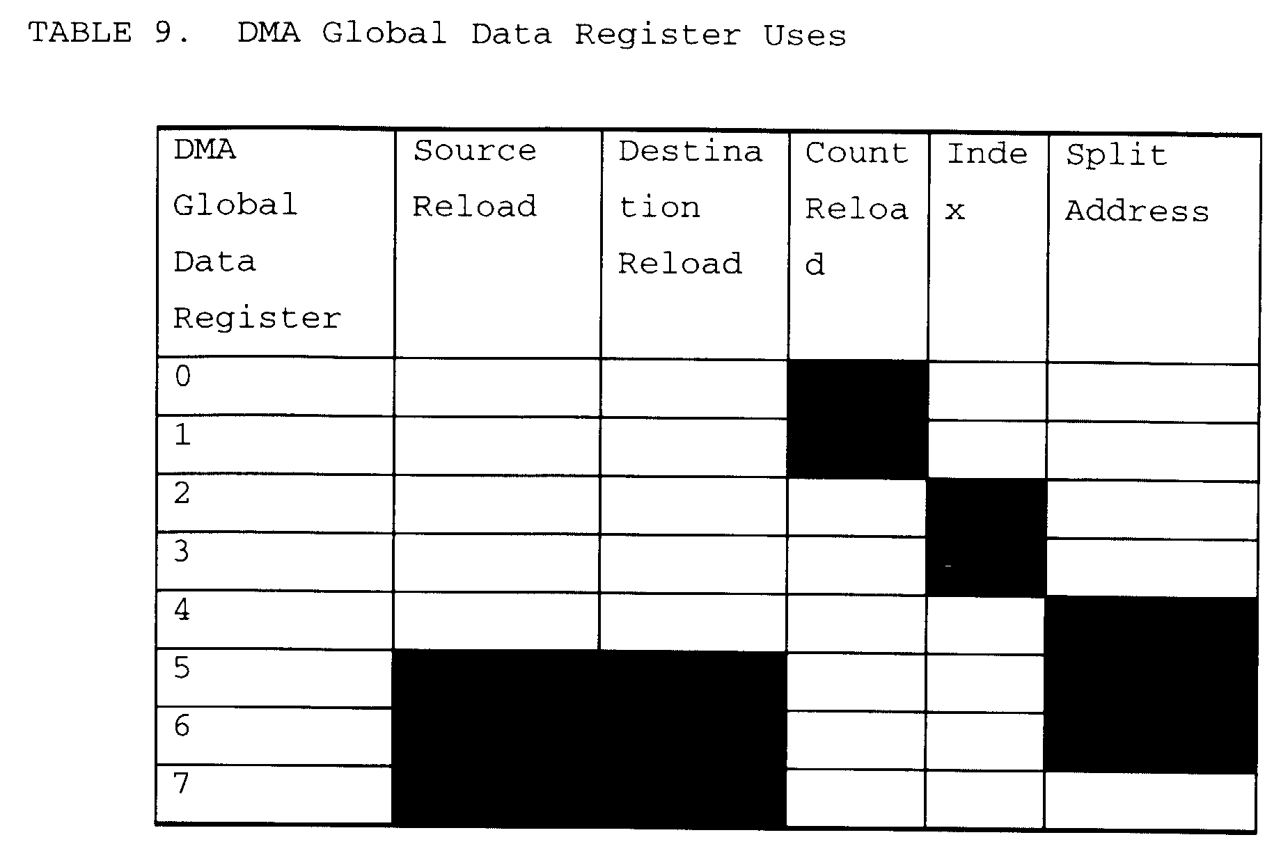
| DMA Channel Primary Control Register Bit Field Definitions | |
| Bitfield | Description |
| START | START=00b, stop START=01b, start, without auto-initialization START=10b, pause START=11b, start with auto-initialization |
| STATUS | STATUS=00b, stopped STATUS=01b, running, without auto-initialization STATUS=10b, paused STATUS=11b, running, with auto-initialization |
| SRC DIR, DST DIR | Source/Destination Address Modification after Element Transfers. (SRC/DST) DIR=00b, no modification. (SRC/DST) DIR=01b, increment by element size in bytes (SRC/DST) DIR=10b, decrement by element size in bytes. (SRC/DST) DIR=11b, adjust using DMA Global Data Register selected by INDEX. |
| RSYNC, WSYNC | Read transfer/write transfer synchronization. (R/W)SYNC=00000b, no synchronization. (R/W)SYNC=other sets synchronization event |
| FS | Frame Synchronization FS=0, disable, FS=1, RSYNC event used to synchronize entire frame. |
| TCINT | Transfer Controller Interrupt . TCINT=0 interrupt disabled TCINT=1 interrupt enabled |
| ESIZE | Element size ESIZE=00b, 32-bit ESIZE=01b, 16-bit ESIZE=10b, 8-bit ESIZE=11b, reserved |
| PRI | Priority Mode: DMA v. CPU PRI=0, CPU priority PRI=1, DMA priority |
| SPLIT | Split channel mode. SPLIT=00b disabled SPLIT=01b, enabled, use DMA SPLIT=10b, enabled, use DMA SPLIT=11b, enabled, use DMA |
| CNT RELOAD | DMA Channel Transfer Counter Reload for Auto-Initialization and Multi-Frame Transfers CNT RELOAD=0, Reload with DMA CNT RELOAD=1, Reload with DMA |
| INDEX | Selects the DMA Global Data Register to use as a programmable index. INDEX=0, use DMA INDEX=1, use DMA |
| EMOD | Emulation Mode EMOD=0, DMA channel keeps running during an emulation halt EMOD=1, DMA channel paused during an emulation halt |
| SRC RELOAD | DMA Channel Source/Destination Address |
| DST RELOAD | Reload for Auto-Initialization SRC/DST RELOAD=00b, do not reload during auto-initialization. SRC/DST RELOAD=01b, use DMA SRC/DST RELOAD=10b, use DMA SRC/DST RELOAD=11b, use DMA |
| DMA Channel Secondary Control Register Bit Fields | ||
| Bit field | Description | |
| SX COND | DMA Condition. See 0 for | |
| FRAME COND | description. | |
| LAST COND | COND=0, condition not detected | |
| BLOCK COND (R/W)DROP COND | COND=1, condition detected | |
| SX IE | DMA Condition Interrupt Enable. | |
| | See | 0 for description. |
| LAST IE | IE=0, associated condition disables | |
| BLOCK IE | DMA channel interrupt | |
| (R/W)DROP | IE=1, associated condition enables | |
| IE | DMA channel interrupt | |
| (R/W)SYNC | Read, Write Synchronization | |
| STAT | Write | |
| 1 to set associated status. | ||
| STAT=0, synchronization not received | ||
| STAT=1, synchronization received | ||
| DMAC EN | DMAC Pin Control | |
| DMAC EN=000b, DMAC pin held low | ||
| DMAC EN=001b, DMAC pin held high | ||
| DMAC EN=010b, DMAC reflects RSYNC | ||
| STAT | ||
| DMAC EN=011b, DMAC reflects WSYNC | ||
| STAT | ||
| DMAC EN=100b, DMAC reflects FRAME | ||
| COND | ||
| DMAC EN=101b, DMAC reflects BLOCK | ||
| COND | ||
| DMAC EN=other, reserved | ||
| (R/W)SYNC | Read, Write Synchronization Status | |
| CLR | Clear | |
| Read as 0, write 1 to clear associated status. |
| Synchronization Events | |||
| Event Number (Binary) | Event Acronym | Event Description | |
| 00000 | None | no synchronization | |
| 00001 | | Timer | 0 Interrupt |
| 00010 | | Timer | 1 Interrupt |
| 00011 | SD_INT | EMIF SDRAM Timer Interrupt | |
| 00100 | EXT_INT4 | External Interrupt | |
| 00101 | EXT_INT5 | External Interrupt | |
| 00110 | EXT_INT6 | External Interrupt | |
| 00111 | EXT_INT7 | External Interrupt | |
| 01000 | | DMA Channel | 0 Interrupt |
| 01001 | | DMA Channel | 1 Interrupt |
| 01010 | | DMA Channel | 2 Interrupt |
| 01011 | | DMA Channel | 3 Interrupt |
| 01100 | | MCSP | 0 Transmit Event |
| 01101 | | MCSP | 0 Receive Event |
| 01110 | | MCSP | 1 Transmit Event |
| 01111 | | MCSP | 1 Receive Event |
| 10000 | DSPINT | Host Port 150Host to DSP Interrupt | |
| Other | Reserved | ||
| Note: in Table 12, MCSP refers to multichannel |
| Sorting Example in Order of DMA Transfers | ||||
| Frame | Element | | Post Adjustment | |
| 0 | 0 | | +6 | |
| 0 | 1 | 0x80000 006 | +6 | |
| 0 | 2 | 0x80000 00C | +6 | |
| 0 | 3 | 0x80000 012 | -16 | |
| 1 | 0 | 0x80000 002 | +6 | |
| 1 | 1 | 0x80000 008 | +6 | |
| 1 | 2 | 0x80000 00E | +6 | |
| 1 | 3 | 0x80000 014 | -16 | |
| 2 | 0 | 0x80000 004 | +6 | |
| 2 | 1 | 0x80000 00A | +6 | |
| 2 | 2 | 0x80000 010 | +6 | |
| 2 | 3 | 0x80000 016 | -16 |
| Sorting Grouping Ordered By Address | |||
| | Element | Address | |
| 0 | 0 | | |
| 1 | 0 | | |
| 2 | 0 | | |
| 0 | 1 | | |
| 1 | 1 | | |
| 2 | 1 | | |
| 0 | 2 | | |
| 1 | 2 | | |
| 2 | 2 | | |
| 0 | 3 | | |
| 1 | 3 | | |
| 2 | 3 | 0x80000016 |
| DMA Global Control Register | |
| Bit field | Description |
| CH PRI | DMA Channel Priority CH PRI=0000b, fixed channel priority mode auxiliary channel 1st highest priority CH PRI=0001b, fixed channel priority mode auxiliary channel 2nd highest priority CH PRI=0010b, fixed channel priority mode auxiliary channel 3rd highest priority CH PRI=0011b, fixed channel priority mode auxiliary channel 4th highest priority CH PRI=0100b, fixed channel priority mode auxiliary channel 5th highest priority CH PRI=other, reserved |
| AUXPRI | Auxiliary Channel Priority Mode AUXPRI=0, CPU priority AUXPRI=1, DMA priority |
| DMA Channel Condition Descriptions | ||||
| Bit field | Event | Occurs if... | COND Cleared By | |
| Name | If IE Enabled | Otherwise | ||
| SX | Split Transmit Overrun Receive | The split operation is enabled and transmit element transfers get seven or more element transfers a ahead of receive element transfers. | A user write of 0 to COND transfers. | |
| FRAM E | Frame Complete | After the last write transfer in each frame is written to memory. | A user write of 0 to COND. | Two CPU clocks later. |
| LAST | Last Frame | After all counter adjustments for the next to last frame in a block transfer complete. | A user write of 0 to COND. | Two CPU clocks later. |
| WDRO P RDRO P | Dropped Read/Write Synchron ization | A subsequent synchronization event occurs before the last one is cleared. | A user write of 0 to COND. | |
| BLOC K | Block Transfer Complete | After the last write transfer in a block transfer is written to memory. | A user write of 0 to COND. | Two CPU clocks later. |
| HPI External Interface Signals | ||||
| Signal Name | Signal Type (Input/Output/HI-Z) | Sig nal Count | Host Connection | Signal Function |
| HD15:0 | I/O/ | 16 | Data Bus | |
| HCNTL1 :0 | I | 2 | Address or control lines | Controls HPI access type. |
| HHWIL | I | 1 | Address or control lines | Halfword identification input. |
| HAS- | I | 1 | Address latch enable (ALE) or Address strobe or unused (tied high)ÁÁÁ | Differentiates address versus data values on multiplexed address/data host. |
| HBE-1:0 | I | 2 | Byte enables | Data write byte enables |
| HR/W- | | 1 | Read/Write strobe, address line, or multiplexed address/ data | Read/Write select |
| HCS- | I | 1 | Address or control lines | Data strobe inputs. |
| HDS1-HDS2- | | 2 | Read strobe and write strobe or data strobe | Data strobe inputs. |
| HRDY- | | 1 | Asynchronous ready | Ready status of current HPI access |
| HINT- | | 1 | Host interrupt input. | Interrupt signal to Host |
| HPI Input Control Signals Function | ||
| HCNTL | ||
| 1 | | |
| 0 | 0 | Host can read or write the HPI control register, HPIC. |
| 0 | 1 | Host can read or write the address register, HPIA. |
| 1 | 0 | Host can read or write HPID. HPIA is postincremented by a word address (4 byte addresses). |
| 1 | 1 | Host can read or write HPID. HPIA is not affected. |
| Byte Enables for HPI Data Write Access | ||||
| Data Write Type | HBE-1:0 | Effective Address LSBs | Logical (binary) | |
| Second Write HHWIL=1 | First Write HHWIL=0 | Little Endian | | |
| Byte | ||||
| 11 | 10 | 00 | 11 | |
| | 11 | 01 | 01 | 10 |
| | 10 | 11 | 10 | 01 |
| | 01 | 11 | 11 | 00 |
| | 11 | 00 | 00 | 10 |
| Halfword | 00 | 11 | 10 | 00 |
| Word | 00 | 00 | 00 | 00 |
| HPI Register Description | ||||
| Register Acronym | Register Name | Host Read/Write | CPU Read/Write | CPU Read/Write (Hex Byte Address) |
| HPID | HPI Data | RW | - | - |
| HPIA | HPI Address | RW | - | - |
| HPIC | HPI Control | RW | RW | 0188 0000 |
| HPI Control Register (HPIC) Bit Descriptions | ||
| Bit | Description | Section |
| HWOB | Halfword Ordering Bit. If HWOB = 1, first halfword is least significant. If HWOB = 0, first halfword is most significant. HWOB affects both data and address transfers. Only the host can modify this bit. HWOB must be initialized before the first data or address register access. | |
| DSPINT | The host processor-to-CPU/DMA interrupt. | 5.3.3. 1 |
| HINT | DSP to Host Interrupt. Determines the state of the CPU HINT- output. | 5.3.3. 2 |
| HRDY | Ready signal to host. Not masked by HCS-like HRDY- pin. If HRDY=0 this indicates that the internal bus is waiting for a HPI data access request to complete. | 5.3.2 |
| FETCH | Host Fetch request. If the host writes a one to this bit, it requests a fetch into HPID the word at the address pointed to by HPIA. Always read as 0. | 5.3.2 |
- If this was a read with post increment,
goto 4. - For a read from the same location, goto 3.
- For a read to a different address,
goto 2.
- For another write operation,
goto 1.
| Initialization of HWOB=1 and HPIA | ||||||||
| Event | Value During Access | Value After Access | ||||||
| HD | HBE-1:0 | HR/W- | HCNTL 1:0 | HHWI L | HPID | HPIC | HPIA | |
| Host writes HPIC 1st halfword | 00 01 | | 0 | 00 | 0 | 00090 009 | ????? ??? | ???? ???? |
| Host writes HPIC 2nd halfword | 00 01 | | 0 | 00 | 1 | 00090 009 | ????? ??? | ???? ???? |
| Host writes HPIA 1st halfword | 12 34 | | 0 | 01 | 0 | 00090 009 | ????1 234 | ???? ???? |
| Host writes HPIA 2nd halfword | 80 00 | | 0 | 01 | 1 | 00090 009 | 80001 234 | ???? ???? |
| Initialization of HWOB=0 and HPIA | ||||||||
| Event | Value During Access | Value After Access | ||||||
| HD | HBE-1:0 | HR/W- | HCNTL 1:0 | HHWI L | HPIA | HPIC | HPID | |
| Host writes HPIC 1st halfword | 0000 | | 0 | 00 | 0 | 00080 008 | ????? ??? | ???? ???? |
| Host writes HPIC 2nd halfword | 0000 | | 0 | 00 | 1 | 00080 008 | ????? ??? | ???? ???? |
| Host writes HPIA 1st halfword | 8000 | | 0 | 01 | 0 | 00080 008 | 8000? ??? | ???? ???? |
| Host writes HPIA 2nd halfword | 1234 | | 0 | 01 | 1 | 00080 008 | 80001 234 | ???? ???? |
| Read Access to HPI Without Auto-Increment: HWOB=1 | ||||||||||
| Event | Value During Access | Value After Access | ||||||||
| HD | HBE-1:0 | HR /W- | HCNT L1:0 | HRD Y- | HHWI L | HPIC | HPIA | HPID | ||
| Host reads 1st halfword Data Not Ready | ???? | | 1 | 11 | 1 | 0 | 00010001 | 80001234 | ???? ???? | |
| Host read 2nd halfword Data | BCDE | xx | 1 | 11 | 0 | 0 | 00090009 | 80001234 | 789A BCDE | |
| Host reads 2nd halfword | 789A | xx | 1 | 11 | 0 | 1 | 00090009 | 80001234 | 789A BCDE |
| Read Access to HPI Without Auto-Increment: HWOB=0 | ||||||||||
| Event | Value During Access | Value After Access | ||||||||
| HD | HBE-1:0 | HR/W- | HCNT L1:0 | HRDY- | HHWIL | HPIC | HPIA | HPI D | ||
| Hos t reads 1st halfword Data Not Ready | ???? | | 1 | 11 | 1 | 0 | 00000000 | 80001234 | ??? ??? ?? | |
| Host read 2nd halfword Data | 789A | xx | 1 | 11 | 0 | 0 | 00080008 | 80001234 | 789 ABCDE | |
| Host reads 2nd halfword | BCDE | xx | 1 | 11 | 0 | 1 | 00080008 | 80001234 | 789 ABCDE |
| Read Access to HPI With Auto-Increment: HWOB=1 | ||||||||||
| Event | Value During Access | Value After Access | ||||||||
| HD | HB E-1: 0 | HR /W- | HC NT L1:0 | HR DY- | H H W I L | HPIC | HPIA | HPID | ||
| Host reads 1st halfword Data Not Ready | ???? | Xx | 1 | 10 | 1 | 0 | 00010001 | 80001234 | ???????? | |
| Host read 2nd halfword Data | BCDE | Xx | 1 | 10 | 0 | 0 | 00090009 | 80001234 | 789ABCDE | |
| Host reads 2nd | 789A | Xx | 1 | 10 | 0 | 1 | 00090009 | 80001238 | 789ABCDE | |
| Pre-fetch Data Not Read | ???? | Xx | x | xx | 0 | x | 00010001 | 80001238 | 789ABCDE | |
| Pre-fetch Data Ready | ???? | Xx | x | xx | 0 | x | 00090009 | 8000123 8 | 87654321 |
| Read Access to HPI With Auto-Increment: HWOB=0 | ||||||||||
| Event | Value During Access | Value After Access | ||||||||
| HD | HBE-1:0 | HR/W- | HCNTL1:0 | HRDY- | HHWIL | HPIC | HPIA | HPID | ||
| Host reads 1st halfword Data Not Ready | ???? | Xx | 1 | 10 | 1 | 0 | 00000000 | 80001234 | ???????? | |
| Host read 2nd halfword Data | 789A | Xx | 1 | 10 | 0 | 0 | 00080008 | 80001234 | 789ABCDE | |
| Host reads 2nd | BCDE | Xx | 1 | 10 | 0 | 1 | 00080008 | 80001238 | 789ABCDE | |
| Pre-fetch Data Not Read | ???? | Xx | x | xx | 0 | x | 00000000 | 80001238 | 789ABCDE | |
| Pre- fetch Data Ready | ???? | X x | x | xx | 0 | x | 00080008 | 80001238 | 87654321 |
| Write Access to HPI Without Auto-Increment: HWOB=1 | |||||||||||
| Event | Value During Access | Value After Access | |||||||||
| HD | HBE-1:0 | HR/W- | HCNTL1:0 | HRDY- | HHWIL | HPIC | HPIA | HPID | Location 80001234 | ||
| Host writes HPID 1st halfword Waiting for Previous | 5566 | 00 | 0 | 11 | 1 | 0 | 00010001 | 80001234 | ????5566 | 00000000 | |
| Host wrotes | 5566 | 00 | 0 | 11 | 0 | 0 | 00090009 | 80001234 | ????5566 | 00000000 | |
| Host writes | wxyz | 11 | 0 | 11 | 0 | 1 | 00090009 | 80001234 | wxyz5566 | 00005566 |


| Write Access to HPI With Auto-Increment: HWOB=1 | |||||||||||
| Event | Value During Access | Value After Access | |||||||||
| HD | HBE-1:0 | HR/W- | HCNTL1:0 | HRDY- | HHWIL | HPIC | HPIA | HPID | Location 80001234 | Location 80001238 | |
| Host writes HPID 1st halfword Waiting for Previous | 5566 | 00 | 0 | 10 | 1 | 0 | 00010001 | 80001234 | ????5566 | 00000000 | 00000000 |
| Host wrotes HPID 1st halfword Ready | 5566 | 00 | 0 | 10 | 0 | 0 | 00090009 | 80001234 | ????5566 | 00000000 | 00000000 |
| Host writes HPIA 2nd halfword | wxyz | 11 | 0 | 10 | 0 | 1 | 00090009 | 80001234 | wxyz5566 | 00005566 | 00000000 |
| Host writes HPID 1st halfword Waiting for Previous | nopq | 11 | 0 | 10 | 1 | 0 | 00010001 | 80001234 | wxyznopq | 00005566 | 00000000 |
| Host writes HPID 1st halfword Ready | nopq | 11 | 0 | 10 | 0 | 1 | 00090009 | 80001238 | wxyznopq | 00005566 | 00000000 |
| Host writes HPIA 2nd halfword | 33rs | 01 | 0 | 10 | 0 | 1 | 00090009 | 80001238 | 33rsnopq | 00005566 | 33000000 |
| Write Access to HPI Without Auto-Increment WHOB=0 | |||||||||||
| Event | Value During Access | Value After Access | |||||||||
| HD | HBE-1:0 | HR/W- | HCNTL1:0 | HRDY- | HHWIL | HPIC | HPIA | HPID | Location 80001234 | Location 80001 238 | |
| Host writes HPID 1st halfword Waiting for Previous | 5566 | 00 | 0 | 10 | 1 | 0 | 00000000 | 800012 34 | ????5566 | 00000000 | 00000000 |
| Host wrotes HPID 1st halfword Ready | 5566 | 00 | 0 | 10 | 0 | 0 | 00080008 | 80001234 | ????5566 | 00000000 | 00000000 |
| Host writes HPIA 2nd | wxyz | 11 | 0 | 10 | 0 | 1 | 00080008 | 80001234 | wxyz5566 | 00005566 | 00000000 |
| halfword | |||||||||||
| Host writes HPID 1st halfword Waiting for Previous | 33rs | 11 | 0 | 1 0 | 1 | 0 | 0000000 0 | 80 00 12 34 | 33rs5566 | 00005566 | 00000000 |
| Host writes HPID 1st halfword Ready | 33rs | 11 | 0 | 1 0 | 0 | 1 | 0008000 8 | 80 00 12 38 | 33rs5566 | 00005566 | 00000000 |
| Host writes HPIA 2nd halfword | nopq | 01 | 0 | 1 0 | 0 | 1 | 0008000 8 | 80 00 12 38 | 33rsnopq | 00005566 | 33000000 |
| EMIF Signal Descriptions | ||
| Pin | (I/O/Z) | Description |
| CLKOU T1 | O | Clock. Clock output - the CPU clock rate. |
| CLKOU T2 | O | Clock. Clock output - ½ the CPU clock rate. |
| ED(31 :0) | I/O /Z | Data I/O. 32-bit data input/output from external memories and peripherals. |
| EA(21 :2) | O/Z | External Address output. Drives bits 21-2 of the byte address. |
| /CEO | O/Z | External /CEO Chip Select. Active low chip select for |
| /CE1 | O/Z | External /CE1 Chip Select. Active low chip select for |
| /CE2 | O/Z | External /CE2 Chip Select. Active low chip select for |
| /CE3 | O/Z | External /CE3 Chip Select. Active low chip select for |
| /BE (3 :0) | O/Z | Byte Enables. Active low byte strobes. Individual bytes and halfwords can be selected for both read and write cycles. Decoded from 2 LSBs of the byte address. |
| /ARDY | I | Ready. Active low asynchronous ready input used to insert wait states for slow memories and peripherals. |
| /AOE | O/Z | Output Enable. Active low output enable for asynchronous memory interface. |
| /AWE | O/Z | Write Strobe. Active low write strobe for asynchronous memory interface. |
| /ARE | O/Z | Read Strobe. Active low read strobe for asynchronous memory interface. |
| /SSAD S | O/Z | Address Strobe. Active low address strobe/enable for SBSRAM interface. |
| /SSOE | O/Z | Output Enable. Output buffer enable for SBSRAM interface. |
| /SSWE | O/Z | Write Enable. Active low write enable for SBSRAM interface. |
| SSCLK | O/Z | Clock. SBSRAM interface clock; equivalent to CLKOUT1 or CLKOUT2 as selected by the user. |
| /SDRA S | O/Z | Row Address Strobe. Active low /RAS for SDRAM memory interface. |
| /SDCA S | O/Z | Column Address Strobe. Active low /CAS for SDRAM memory interface. |
| /SDWE | O/Z | Write Enable. Active low /W for SDRAM memory interface. |
| SDA10 | O/Z | SDRAM A10 Address Line. Address line/auto-precharge disable for SDRAM memory. |
| SDCLK | O/Z | Clock. SDRAM interface clock- ½ the CPU clock rate. Equivalent to CLKOUT2. |
| /HOLD | I | Hold. Active low external bus hold (tristate) request. |
| /HOLD A | O | Hold Acknowledge. Active low external bus hold acknowledge. |
| EMIF Memory Mapped Registers | |
| Byte Address | Name |
| 0x01800000 | EMIF Global Control |
| 0x01800004 | EMIF CE1 Space Control |
| 0x01800008 | EMIF CE0 Space Control |
| 0x0180000C | Reserved |
| 0x01800010 | EMIF CE2 Space Control |
| 0x01800014 | EMIF CE3 Space Control |
| 0x01800018 | EMIF SDRAM Control |
| 0x0180001C | EMIF SDRAM Refresh Period |
| EMIF Global Control Register Bit Field Description | |
| Field | Description |
| SDCINV | SDCLK polarity SDCINV = 0, SDCLK output is inverted from internal SDCLK SDCINV = 1, SDCLK output is identical to internal SDCLK |
| CLK2INV | CLKOUT2 polarity CLK2INV = 0, CLKOUT2 output is inverted from internal CLKOUT2 CLK2INV = 1, CLKOUT2 output is identical to internal CLKOUT2 |
| /ARDY | Value of /ARDY input |
| /HOLD | Value of /HOLD input |
| /HOLDA | Value of /HOLDA output |
| NOHOLD | External HOLD disable (1 = hold disabled; 0 = hold enabled) |
| SDCEN | SDCLK enable SDCEN =0, SDCLK held high SDCEN =1, SDCLK enabled to clock |
| SSCEN | SSCLK enable SSCEN=0, SSCLK held high SSCEN=1, SSCLK enabled to clock |
| CLK1EN | CLKOUT1 enable CLK1EN=0, CLKOUT1 held high CLK1EN=1, CLKOUT1 enabled to clock |
| CLK2EN | CLKOUT2 enable CLK2EN=0, CLKOUT2 held high CLK2EN=1, CLKOUT2 enabled to clock |
| SSCRT1 | SBSRAM clock rate select SSCRT=0, SSCLK ½x CPU clock rate SSCRT=1, SSCLK 1x CPU clock rate |
| RBTR8 | Requester arbitration mode RBTR8=0, requester controls EMIF until a high priority request occurs RBTR8=1, requester controls EMIF for a minimum of eight accesses |
| MAP | Map mode, contains the value of the memory map mode of the device |
| EMIF CE(0/1/2/3) Space Control Registers Bitfield Description | |
| Field | Description |
| READ SETUP WRITE SETUP | Setup width. Number of CLKOUT1 cycles of setup for address (EA) and byte enables (/BE(0-3)) before read strobe (/ASRE) or write strobe (/ASWE) falling. On the first access to a CE space this is also the setup after /CE falling. |
| READ STROBE WRITE STROBE | Strobe width. The width of read strobe (/ASRE) and write strobe (/ASWE) in CLKOUT1 cycles. |
| READ HOLD RITE HOLD | Hold width. Number of CLKOUT1 cycles that address (EA) and byte strobes (/BE(0-3)) are held after read strobe (/ASRE) or write strobe (/ASWE) rising. |
| TA | Turn-around width. The number of CLKOUT1 cycles between reads and writes or between accesses to different CE spaces. Measured from when /OE rises. One turn-around cycle is inserted between a write followed by a read. One turn-around cycle is inserted between consecutive accesses to two different CE spaces from the same requester. TA=00b, 1 turn-around cycle. TA=01b, 2 turn-around cycles. TA=10b, 3 turn-around cycles. TA=11b, 4 turn-around cycles. |
| MTYPE | Memory Type. MTYPE=000b, 8-bit MTYPE=001b, 16-bit MTYPE=010b, 32-bit wide Asynchronous Interface MTYPE=011b, 32-bit MTYPE=100b, 32-bit wide SBSRAM |
| MTYPE=other, reserved |
| EMIF SDRAM Control Register Bitfield Description | |
| Field | Description |
| TRC | Specifies t RC value of the SDRAM in CLKOUT2 cycles. TRC = t RC - 1. |
| TRP | Specifies t RP value of the SDRAM in CLKOUT2 cycles. TRP = t RP - 1. |
| TRCD | Specifies t RCD value of the SDRAM in CLKOUT2 cycles. TRCD = t RCD - 1. |
| INIT | Forces an initialization of all SDRAM present. See section 6.3.1. |
| INIT = 0, no effect. | |
| NIT = 1, initialize SDRAM in each CE space configured for SDRAM. | |
| RFEN | Refresh Enable. |
| RFEN = 0, SDRAM refresh disabled. | |
| RFEN = 1, SDRAM refresh enabled. | |
| SDWID | SDRAM Width Select |
| SDWID=0, Each External SDRAM Space Consists of 4 8-bit SDRAMs | |
| SDWID=1, Each External SDRAM Space Consists of 2 16-bit SDRAMs |
| EMIF SDRAM Timing Register Bitfield Description | |
| Field | Description |
| PERIOD | Refresh period in CLKOUT2 cycles. |
| COUNTER | Current value of the refresh counter. |
| EMIF SDRAM Commands | |
| Command | Function |
| DCAB | Deactivate (also known as pre-charge) all banks |
| ACTV | Activate the selected bank and select the row |
| READ | Input the starting column address and begin the read operation |
| WRT | Input the starting column address and begin the write operation |
| MRS | Mode Register Set, configures SDRAM mode register |
| REFR | Auto refresh cycle with internal address |
| SDRAM Memory Population | ||||
| SDRAM size | SDRAM banks | SDRAM width | Devices per CE space | Memory Size per |
| 16 Mbit | 2 | 16 | 2 | 4 Mbytes |
| 16 Mbit | 2 | 8 | 4 8 Mbytes | |
| 64 Mbit | 4 | 16 | 2 | 16 Mbytes |
| SDRAM Control Pins | ||
| EMIF Signal | SDRAM Signal | SDRAM Function |
| SDA10 | A10 | Address line A10/auto-precharge disable. Serves as a row address bit during ACTV commands and also disables the auto-pre-charging function of SDRAM. |
| /SDRAS | /RAS | Row Address Strobe and Command Input. Latched by the rising CLK to determine current operation. Only valid if /CS is active- low during that clock edge. |
| /SDCAS | /CAS | Column Address Strobe and Command Input. Latched by the rising CLK to determine current operation. Only valid if /CS is active- low during that clock edge. |
| /SDWE | /WE | W rite Strobe and Command Input. Latched by the rising CLK to determine current operation. Only valid if /CS is active- low during that clock edge. |
| /BE[3:0] | DQM[3:0] | Data / output mask. DQM is an input/output buffer control signal. It disables writes and tri-states outputs during reads when high. DQM has a 2 CLK latency on reads and a 0 CLK latency on writes. DQM pins serve essentially as byte strobes and are connected to /BE[3:0] outputs. |
| /CE3 or /CE2 or /CE0 | /CS | Chip select and command enable. /CS must be active-low for a command to be clocked into the SDRAM. /CS does not affect data input or output once a write or read has begun. |
| - | CKE | CKE clock enable. Tied active high when interface to EMIF to always enable clocking. |
| CLKOUT2 | CLK | SDRAM clock input. Runs at ½ the CPU clock rate. |
| SDCLK | CLK | SDRAM clock input. Runs at ½ the CPU clock rate. Equivalent to CLKOUT2. |
| Mode Register Value | ||||||||||||||
| | 13 | 12 | 1 1 | 10 | 9 | 8 | 7 | 6 | 5 | 4 | 3 | 2 | 1 | 0 |
| EMIF Pins | | | EA13 | SDA10 | EA11 | EA10 | EA9 | EA8 | EA7 | EA6 | EA5 | EA4 | EA3 | EA2 |
| Field | Reserved | Write Burst Length | Reserved | Read Latency | S/I | | ||||||||
| Value | ||||||||||||||
| 0 | 0 | 0 | 0 | 0 | 0 | 0 | 0 | 1 | 1 | 0 | 0 | 0 | 0 |
| Implied SDRAM Configuration by MRS Value | |
| Field | Selection |
| | 1 |
| | 3 |
| Serial/Interlea ve Burst Type | |
| Burst Length | |
| 1 |

| SDRAM Timing Parameters | ||
| Parame ter | Description | Value in CLKOUT2 Cycles |
| tRC | REFR command to ACTV, MRS, or subsequent REFR command | TRC + 1 |
| tRCD | ACTV command to READ or WRT command | TRCD + 1 |
| tRP | DCAB command to ACTV, MRS, or REFR command | TRP +1 |
| tRAS | ACTV command to DEAC to DCAB command | 7 |
| tnEP | Overlap between read data and a | 2 |
| EMIF SBSRAM Pins | ||
| EMIF Signal | SBSRAM Signal | SBSRAM Function |
| SSADS | /ADS | Address Strobe. |
| /SSOE | /OE | Output Enable |
| /SSWE | /WE | Write Enable |
| SSCLK | CLK | SBSRAM Clock |
| EMIF Asynchronous Interface Pins | |
| EMIF Signal | Function |
| /AOE | Output Enable - active low during the entire period of a read access. |
| /AWE | Write Enable - active low during a write transfer strobe period. |
| /ARE | Read Enable - active low during a read transfer strobe period. |
| /ARDY | Ready input used to insert wait states into the memory cycle. |
| width | EA22 | EA21 | EA20 | EA19 | EA18 | EA17 | EA16 | EA15 | EA14 | EA13 | EA12 | EA11 | EA10 | EA9 | EA8 | EA7 | EA6 | EA5 | EA4 | | EA2 |
| x3 | |||||||||||||||||||||
| 2 | 22 | 21 | 20 | 19 | 18 | 17 | 16 | 15 | 14 | 13 | 12 | 11 | 10 | 9 | 8 | 7 | 6 | 5 | 4 | 3 | 2 |
| | 21 | 20 | 19 | 18 | 17 | 16 | 15 | 14 | 13 | 12 | 11 | 10 | 9 | 8 | 7 | 6 | 5 | 4 | 3 | 2 | 1 |
| | 20 | 19 | 18 | 17 | 16 | 15 | 14 | 13 | 12 | 11 | 10 | 9 | 8 | 7 | 6 | 5 | 4 | 3 | 2 | 1 | 0 |
- /CE becomes active low.
- /AOE becomes active low.
- /BE[3:0] becomes valid.
- EA becomes valid.
- /ARE is pulled active low.
- /ARE is pulled inactive high
- Data is sampled on the CLKOUT1 rising edge concurrent with the beginning of the hold period (end of the strobe period), just prior to the /ARE low-to-high transition.
- /CE becomes inactive as long as another read access to the same /CE space is not scheduled for the next cycle.
- /AOE becomes inactive as long as another read access to the same /CE space is not scheduled for the next cycle.
- /CE becomes active low.
- /BE[3:0] becomes valid.
- EA becomes valid.
- ED becomes valid.
- /AWE becomes inactive low.
- /AWE becomes inactive high
- Data is sampled on the CLKOUT1 rising edge concurrent with the beginning of the hold period (end of the strobe period), just prior to the /AWE low-to-high transition.
- ED becomes tri-state only if as another write access to the same /CE space is NOT scheduled for the next cycle.
- /CE becomes inactive only if another write access to the same /CE space is NOT scheduled for the next cycle.
- If the next access is a read a cycle of turn around is inserted before AOE is enabled.
| EMIF Prioritization of Requests | ||
| Priority | Requester PRI=1 | Requester PRI=0 |
| Highest | External Hold | |
| Mode Register | ||
| Set | ||
| Urgent | ||
| Refresh | ||
| DMA | DMC | |
| DMC | PMC | |
| PMC | DMA | |
| Lowest | Trickle | |
| Refresh |
| Boot Configurations | |||
| BOOT MODE [4:0] | Memory Map | Memory At Address 0 | Boot Process |
| 00000 | MAP 0 | SDRAM 4 banks of 8-bit (SWID=0) | none |
| 00001 | MAP 0 | SDRAM 2 banks of 16-bit (SWID=1) | none |
| 00010 | MAP 0 | 32-Bit Asynchronous w/Default Timing | none |
| 00011 | MAP 0 | ½ Rate SBSRAM | none |
| 00100 | MAP 0 | lx Rate SBSRAM | none |
| 00101 | MAP 1 | Internal | none |
| 00110 | MAP 0 | External, Default Values | HPI |
| 00111 | MAP 1 | Internal | HPI |
| 01000 | MAP 0 | SDRAM 4 banks of 8-bit (SWID=0) | 8-bit ROM w/default timings |
| 01001 | MAP 0 | SDRAM 2 banks of 16-bit (SWID=1) | 8-bit ROM w/default timings |
| 01010 | MAP 0 | 32-Bit Asynchronous w/Default Timing | 8-bit ROM w/default timings |
| 01011 | MAP 0 | ½ Rate SBSRAM | 8-bit ROM w/default timings |
| 01100 | MAP 0 | lx Rate SBSRAM | 8-bit ROM w/default timings |
| 01101 | MAP 1 | Internal | 8-bit ROM w/default timings |
| 01110 | Reserved | ||
| 01111 | Reserved | ||
| 10000 | MAP 0 | SDRAM 4 banks of 8-bit (SWID=0) | 16-bit ROM w/default timings |
| 10001 | MAP 0 | SDRAM 2 banks of 16-bit (SWID=1) | 16-bit ROM w/default timings |
| 10010 | MAP 0 | 32-Bit Asynchronous w/Default Timing | 16-bit ROM w/default timings |
| 10011 | MAP 0 | ½ Rate SBSRAM | 16-bit ROM w/default timings |
| 10100 | MAP 0 | lx Rate SBSRAM | 16-bit ROM w/default timings |
| 10101 | MAP 1 | Internal | 16-bit ROM w/default timings |
| 10110 | Reserved | ||
| 10111 | Reserved | ||
| 11000 | MAP 0 | SDRAM 4 banks of 8-bit (SWID=0) | 32-bit ROM w/default timings |
| 11001 | MAP 0 | SDRAM 2 banks of 16-bit (SWID=1) | 32-bit ROM w/default timings |
| 11010 | MAP 0 | 32-Bit Asynchronous w/Default Timing | 32-bit ROM w/default timings |
| 11011 | MAP 0 | ½ Rate SBSRAM | 32-bit ROM w/default timings |
| 11100 | MAP 0 | 1x Rate SBSRAM | 32-bit ROM w/default timings |
| 11101 | MAP 1 | Internal | 32-bit ROM w/default timings |
| 11110 | Reserved | ||
| 11111 | Reserved |
| Memory Map | ||||
| Address (Hex) | Range | Size (bytes) | | |
| 00000000 | | 4M | External Memory Interface - | Internal Program RAM |
| 00400000 | 00FFFFFF | 12M | External Memory Interface - | |
| 01000000 | | 4M | | |
| 4M | - | |||
| 01400000 | 017FFFFF | 256K | Internal Program RAM | External Memory Interface - |
| 256K | ||||
| 01800000 | 0183FFFF | 256K | Internal Peripheral Bus -EMIF Registers | |
| 01840000 | 0187FFFF | 256K | Internal Peripheral Bus -DMA Controller Registers | |
| 01880000 | 018BFFFF | 256K | Internal Peripheral Bus -HPI Register | |
| 018C0000 | 018FFFFF | 256K | Internal Peripheral Bus - | |
| 01900000 | 0193FFFF | 256K | Internal Peripheral Bus - | |
| 01940000 | 0197FFFF | 256K | Internal Peripheral Bus - | |
| 01980000 | 019BFFFF | 256K | Internal Peripheral Bus - | |
| 019C0000 | 019FFFFF | 256K | Internal Peripheral Bus -Interrupt Selector Registers | |
| 01A00000 | 01FFFFFF | 6M | Internal Peripheral Bus - Reserved | |
| 02000000 | | 16M | External Memory Interface - | |
| 03000000 | | 16M | External Memory Interface - | |
| 04000000 | 7FFFFFFF | 2G-64M | Reserved | |
| 80000000 | | 4M | Internal Data RAM | |
| 80400000 | FFFFFFFF | 2G-4M | Reserved |
- 1. Direct interface to:
- T1/E1 framers
- MVIP and ST-BUS compliant devices
- IOM-2 compliant devices
- AC97 compliant devices. The necessary multi-phase frame synchronization capability is provided.
- IIS compliant devices
- SPI devices
| MCSP Interface Signals | ||
| Pin | I/O/Z | Description |
| CLKR | I/O/Z | Receive clock |
| CLKX | I/O/Z | Transmit clock |
| CLKS | I | External clock |
| DR | I | Received serial data |
| DX | O/Z | Transmitted serial data |
| FSR | I/O/Z | Receive frame synchronization |
| FSX | I/O/Z | Transmit frame synchronization |
| MCSP Registers | |||
| Hex Byte Address | | ||
| MCSP | |||
| 0 | | Acronym | |
| - | - | RBR | MCSP Receive Buffer Register |
| - | - | RSR | MCSP Receive Shift Register |
| - | - | XSR | MCSP Transmit Shift Register |
| 018C0000 | 01900000 | DRR | MCSP Data Receive Register |
| 018C0004 | 01900004 | DXR | MCSP Data Transmit Register |
| 018C0008 | 01900008 | SPCR | MCSP Serial Port Control Register |
| 018C000C | 0190000C | RCR | MCSP Receive Control Register |
| 018C0010 | 01900010 | XCR | MCSP Transmit Control Register |
| 018C0014 | 01900014 | SRGR | MCSP Sample Rate Generator Register |
| 018C0018 | 01900018 | MCR | MCSP Multi-Channel Register |
| 018C001C | 0190001C | RCER | MCSP Receive Channel Enable Register |
| 018C0020 | 01900020 | XCER | MCSP Transmit Channel Enable Register |
| 018C0024 | 01900024 | PCR | MCSP Pin Control Register |
| MCSP CPU Interrupts and DMA Event Synchronization | |
| Interrupy Name | Description |
| RINT | Receive Interrupt to CPU |
| XINT | Transmit Interrupt to CPU |
| REVT | Receive Synchronization Event to DMA |
| XEVT | Transmit Synchronization Event to DMA |
| Serial Port Control Register (SPCR) Bit-Field Description | |
| Name | Function |
| DX STAT | DX pin status. Reflects value driven on to DX pin when selected as a general purpose output. |
| DR STAT | DR pin status. Reflects value on DR pin. |
| RIOEN XIOEN | Receive/Transmit General Purpose I/O Mode (R/X)IOEN=0, DR/DX pin is not a general purpose I/O (R/X)IOEN=1, DR/DX pin used as general purpose I/O |
| CLKSTP | Clock Stop Mode CLKSTP=000b, Clock Stop Mode Disabled CLKSTP=100b, Clock starts with rising edge without delay CLKSTP=101b, Clock starts with rising edge with delay CLKSTP=110b, Clock starts with falling edge without delay CLKSTP=111b, Clock starts with falling edge with delay CLKSTP=other, reserved |
| DLB | Digital Loop Back Mode DLB = 0, Digital loop back mode disabled DLB = 1, Digital loop back mode enabled |
| RJUST | Receive Sign-Extension and Justification Mode RJUST=00b, right-justify and zero-fill MSBs in DRR RJUST=01b, right-justify and sign-extend MSBs in DRR RJUST=10b, left-justify and zero-fill LSBs in DRR RJUST=11b, reserved |
| RINTM XINTM | Receive/Transmit Interrupt mode (R/X)INTM=00b, (R/X)INT driven by (R/X)RDY (R/X)INTM=01b, (R/X)INT generated by new block in multi-channel mode (R/X)INTM=10b, (R/X)INT generated by a new frame synchronization (R/X)INTM=11b, (R/X)INT generated by (R/X) SYNCERR |
| RSYNCERR XSYNCERR | Receive/Transmit Synchronization Error (R/X)SYNCERR=0, no synchronization error (R/X)SYNCERR=1, synchronization error detected by MCSP. |
| RFULL | Receive Shift Register (RSR) Full RFULL = 0, RBR is not full RFULL = 1, RBR is full and DRR is not read |
| XEMPTY- | Transmit Shift Register (XSR) Empty XEMPTY- = 0, XSR is empty XEMPTY- = 1, XSR is not empty |
| RRDY XRDY | Receiver/Transmitter Ready (R/X)RDY=0, receiver/transmitter is not ready. (R/X)RDY=1, receiver is ready with data to be read from DRR or transmitter is ready with data in DXR. |
| RRST- XRST- | Receiver/transmitter reset. This resets and enables the receiver/ transmitter. (R/X)RST- = 0, The serial port receiver/transmitter is disabled and in reset state. (R/X)RST- = 1, The serial port receiver/transmitter is enabled. |
| Pin Control Register (PCR) Bit-Field Description | |
| Name | Function |
| XIOEN RIOEN | Transmit/Receive General Purpose I/O Mode (R/X)IOEN=0, DR pin is not a general purpose input; DX pin is not a general purpose output (R/X)IOEN=1, DR pin is a general purpose input; DX pin is a general purpose output. The serial port pins do not perform serial port operation. |
| FSXM | Transmit Frame Synchronization Mode FSXM = 0, Frame synchronization signal derived from an external source FSXM = 1, Frame synchronization is determined by the Sample Rate Generator frame synchronization mode bit FSGM in the SRGR. |
| FSRM | Receive Frame Synchronization Mode FSRM = 0, Frame synchronization pulses generated by an external device. FSR is an input pin FSRM = 1, Frame synchronization generated internally by sample rate generator. FSR is an output pin except when GSYNC=1 in SRGR. |
| CLKS_ STAT | CLKS pin status. Reflects value driven on to CLKS pin when selected as a general purpose output. |
| DX_STAT | DX pin status. Reflects value driven on to DX pin when selected as a general purpose output. |
| DR_STAT | DR pin status. Reflects value on DR pin when selected as a general purpose input. |
| FSXP FSRP | Receive/Transmit Frame Synchronization Polarity FS(R/X)P = 0, Frame synchronization pulse FS(R/X) is active high FS(R/X)P = 1, Frame synchronization pulse FS(R/X) is active low |
| CLKXP | Transmit Clock Polarity CLKXP = 0, Transmit data sampled on rising edge of CLKX CLKXP = 1, Transmit data sampled on falling edge of CLKX |
| CLKRP | Receive Clock Polarity CLKRP = 0, Receive data sampled on falling edge of CLKR CLKRP = 1, Receive data sampled on rising edge of CLKR |
| Receive/Transmit Control Register (RCR/XCR) Bit-Field Description | |
| Name | Function |
| (R/X) PHASE | Receive/Transmit Phases (R/X)PHASE=0, single phase frame (R/X)PHASE=1, dual phase frame |
| (R/X)FRLEN(1 /2) | Receive/Transmit |
| (R/X)WDLEN(1 /2) | Receive/Transmit |
| RCOMPAND XCOMPAND | Receive/Transmit Companding Mode. Modes other than 00b are only enabled when the appropriate (R/X)WDLEN is 000b, indicating 8-bit data. (R/X)COMPAND=00b, no companding, data transfer starts with MSB first. (R/X)COMPAND=01b, no companding, 8-bit data, transfer starts with LSB first. (R/X)COMPAND=10b, compand using µ-law for receive/transmit data. (R/X)COMPAND=11b, compand using A-law for receive/transmit data. |
| RFIG XFIG | Receive/Transmit Frame Ignore (R/X)FIG = 0, Receive/Transmit Frame synchronization pulses after the first restarts the transfer. (R/X)FIG = 1, Receive/Transmit Frame synchronization pulses after the first are ignored. |
| RDATDLY XDATDLY | Receive/Transmit data delay (R/X)DATDLY=00b, 0-bit data delay (R/X)DATDLY=01b, 1-bit data delay (R/X)DATDLY=10b, 2-bit data delay (R/X)DATDLY=11b, reserved |
| Reset State of MCSP Pins | ||
| MCSP PINS | DEVICE RESET | MCSP RESET |
| Receiver Reset (RRST-=0) | ||
| DR | Hi-Z | Hi-Z Input |
| CLKR | Hi-Z | Hi-Z if Input; CLKRP if Output |
| FSR | Hi-Z | Hi-Z if Input; FSRP(inactive state) if Output |
| CLKS | Hi-Z | Input should be pulled-up or pulled-down ONLY if transmitter is also reset or if the transmitter is configured with CLKSM=1 in SRGR. |
| Transmitter Reset (XRST-=0) | ||
| DX | Hi-Z | Hi-Z Output |
| CLKX | Hi-Z | Hi-Z if Input; CLKXP if Output |
| FSX | Hi-Z | Hi-Z if Input; FSXP(inactive state) if Output |
| CLKS | Hi-Z | Input should be pulled-up or pulled-down ONLY if receiver is also reset or if the receiver is configured with CLKSM=1 in SRGR. |
| SPCR= | Transmitter reset, transmit interrupt (XINT toCPU) generated by XSYNCERR; receiver is running with RINT driven by RRDY. |
| PCR=0x0000 0A00 | FSX determined by FSGM in SRGR, receive clock driven by external source, transmit clock continues to be driven by sample rate generator. |
| SRGR- | CPU clock drives the sample rate generator clock (CLKG) after a divide-by-2. A DXR-to-XSR copy generated the transmit frame sync signal. |
| XCR=0x8421 0840 | Dual phase frame; |
| SPCR= | Transmitter taken out of reset |
| RCR/XCR Bit-fields Controlling Words/Frame and Bits/Word | |||
| Serial Port MCSP0/1 | Frame Phase | RCR/XCR Bit-field Words/Frame | Control Bits/Word |
| Receive | 1 | RFRLEN1 | RWDLEN1 |
| Receive | 2 | RFRLEN2 | RWDLEN2 |
| Transmit | 1 | XFRLEN1 | XWDLEN1 |
| Transmit | 2 | XFRLEN2 | XWDLEN2 |
| MCSP Receive/Transmit | ||||
| (R/X)PHASE | (R/X)FRLE N1 | (R/X)FRL | Frame Length | |
| 0 | 0 ≤ n ≤ 127 | X | Single Phase Frame; (n+1) words per | |
| 1 | 0 ≤ n ≤ 127 | 0 ≤ m ≤ 127 | Dual Phase Frame; (n+1) plus (m+1) words per frame |
| MCSP Receive/Transmit Word Length Configuration | |
| (R/X)WDLEN(1/2) | MCSP Word Length (bits) |
| 000 | 8 |
| 001 | 12 |
| 010 | 16 |
| 011 | 20 |
| 100 | 24 |
| 101 | 32 |
| 110 | reserved |
| 111 | reserved |
| Use of RJUST Field with 12-Bit Example Data 0xABC | ||||
| RJUST | Justification | Extension | Value in DRR | |
| 00 | right | zero- | 0x00000ABC | |
| 01 | right | sign-extend | OxFFFFFABC | |
| 10 | left | zero- | 0xABC00000 | |
| 11 | reserved | reserved | reserved |
| Justification of Expanded Data (LAW16) | |||
| | DRR | ||
| 31 | 15 | ||
| 16 | 0 | ||
| 00 | 0 | | |
| 01 | | LAW16 | |
| 10 | | 0 | |
| 11 | reserved |
| Sample Rate Generator Register (SRGR) Bit-Field Summary | |
| Name | Function |
| GSYNC | Sample rate generator clock synchronization. Only used when the external clock (CLKS) drives the sample rate generator clock (CLKSM=0). GSYNC=0, the sample rate generator clock (CLKG) is always running. GSYNC=1, the sample rate generator clock (CLKG) is synchronized and frame sync signal (FSG) is generated only after detecting the receive frame synchronization signal (FSR). Also, frame period, FPER, is a don't care because the period is dictated by the external frame sync pulse. |
| CLKSP | CLKS Polarity Clock Edge Select. Only used when the external clock CLKS drives the sample rate generator clock (CLKSM=0). CLKSP=0, falling edge of CLKS generates CLKG and FSG. CLKSP=1, rising edge of CLKS generates CLKG and FSG. |
| CLKSM | MCSP Sample Rate Generator Clock Mode CLKSM = 0, Sample rate generator clock derived from the CLKS pin. CLKSM = 1 Sample rate generator clock derived from CPU clock. |
| FSGM | Sample Rate Generator Transmit frame synchronization mode. Used when FSXM=1 in XCR. FSGM=0, Transmit frame sync signal (FSX) due to DXR-to-XSR copy. FSGM=1, Transmit frame sync signal driven by the sample rate generator frame sync signal, FSG. |
| FPER | Frame Period. This determines when the next frame sync signal should become active. |
| FWID | Frame Width. Determines the width of the frame sync pulse, FSG, during its active period. |
| CLKGDV | Sample rate generator clock divider. This value is used as the divide-down number to generate the required sample rate generator clock frequency. |
Note that FPER is not programmed since it is determined by the arrival of the next external frame sync pulse. The figure shows what happens to CLKG when it is initially in sync and GSYNC=1 as well as not in sync with the frame synchronization and GSYNC=1.
| Receive Clock Selection | ||||
| DLB in SPCR | CLKRM in RCR | Source of Receive | CLKR Pin | |
| 0 | 0 | CLKR pin acts as an input driven by external clock and inverted as determined by CLKRP before being used. | | |
| 0 | 1 | Sample Rate Generator Output. Clock (CLKG) drives CLKR. | CLKG inverted as determined by CLKRP before being driven out on CLKR. | |
| 1 | 0 | CLKX_int drives CLKR_int as selected and inverted. | | |
| 1 | 1 | CLKX_int drives CLKR_int as selected and inverted. | Output. CLKR inverted as determined by CLKRP before being driven out. |
| Transmit Clock Selection | |||
| CLKXM in XCR | Source of Transmit | CLKX Pin | |
| 0 | External clock drives the CLKX input pin. CLKX is inverted as determined by CLKXP before being used. | | |
| 1 | Sample rate generator clock, CLKG, drives transmit clock | Output. CLKG inverted as determined by CLKXP before being driven out on CLKX. |
| Receive Frame Synchronization Selection | |||||
| DLB in SPCR | FSRM in PCR | GSYNC in SRGR | Source of Receive Frame | FSR Pin | |
| 0 | 0 | X | External frame sync signal drives the FSR input pin. This is then inverted as determined by FSRP before being used as FSR_int. | | |
| 0 | 1 | 0 | FSR_int driven by Sample Rate Generator Frame Sync signal (FSG) | Output. FSG inverted as determined by FSRP before being driven out on FSR pin. | |
| 0 | 1 | 1 | FSR_int driven by Sample Rate Generator Frame Sync signal (FSG) | Input. The external frame sync input on FSR is used to synchronize CLKG and generate FSG. | |
| 1 | 0 | 0 | FSX_int drives FSR_int. FSX is selected. | High Impedance. | |
| 1 | | 1 | FSX_int drives FSR_int and is selected. | Input. External FSR not used for frame synchroniza-tion but still used to synchro-nize CLKG and generate FSG since GSYNC=1. | |
| 1 | 1 | 0 | FSX_int drives FSR_int and is selected. | Output. Receive (same as transmit) frame synchroniza-tion inverted as determined by FSRP before being driven out. |
| Transmit Frame Synchronization Selection | |||
| FSXM in PCR | FSGM in SRGR | Source of Transmit Frame Synchronization | FSX Pin |
| 0 | X | External frame sync input on FSX pin. This is inverted by FSXP before being used as FSX_int. | Input. |
| 1 | 1 | Sample Rate Generator Frame Sync signal (FSG) drives FSX_int. | Output. FSG inverted by FSXP before being driven out on FSX pin. |
| 1 | 0 | A DXR-to-XSR copy activates transmit frame sync signal. | Output. One bit clock wide signal inverted by FSXP before being driven out on FSX pin. |
| Multi-Channel Control Register Bit-Field Descriptions | |
| Name | Function |
| RMCM | Receive Multi-channel Selection Enable RMCM = 0, all 128 channels enabled. RMCM = 1, all channels disabled by default. Required channels are selected by enabling RP(A/B)BLK and RCER appropriately. |
| XMCM | Transmit Multi-channel Selection Enable XMCM = 00b, all channels enabled without masking (DX is always driven and never placed in a high impedance state). XMCM = 01b, all channels disabled and therefore masked by default. Required channels are selected by enabling XP(A/B)BLK and XCER appropriately. Also, these selected channels are not masked and therefore DX is always driven. XMCM = 10b, all channels enabled, but masked. Selected channels enabled via XP(A/B)BLK and XCER are unmasked. XMCM = 11b, all channels disabled and therefore masked by default. Required channels are selected by enabling RP(A/B)BLK and RCER appropriately. Selected channels can be unmasked by RP(A/B)BLK and XCER. This mode is used for symmetric transmit and receive operation. |
| RCBLK/ XCBLK | Receive/Transmit Current Block. (R/X)CBLK = 000b, (R/X)CBLK = 001b, (R/X)CBLK = 010b, (R/X)CBLK = 011b, (R/X)CBLK = 100b, (R/X)CBLK = 101b, (R/X)CBLK = 110b, (R/X)CBLK = 111b, |
| RPBBLK / XPBBLK | Receive/Transmit Partition B Block. (R/X)PBBLK= 00b, (R/X)PBBLK= 01b, (R/X)PBBLK= 10b, (R/X)PBBLK= 11b, |
| RPABLK / XPABLK | Receive/Transmit Partition A Block. (R/X)PABLK= 00b, (R/X)PABLK= 01b, (R/X)PABLK= 10b, (R/X)PABLK= 11b, |
| Receive/Transmit Channel Enable Register Bit-Field Description | |
| Name | Function |
| (R/X) | Receive/Transmit Channel Enable (R/X)CEA n=0, Disables reception/transmission nth channel in an even-numbered block in partition A (R/X)CEA n=1, Enables reception/transmission of nth channel in an even-numbered block in partition A |
| (R/X) | Receive/Transmit Channel Enable (R/X)CEB n=0, Disables reception/transmission nth channel in odd-numbered block in partition B. (R/X)CEB n=1, Enables reception/transmission of nth channel in odd-numbered block in partition B. |
| Serial Port Clock Scheme | ||
| | Clock Scheme | |
| 000 | Clock | |
| 100 | Low inactive state without delay: The MCSP transmits data on the rising edge of the CLKX and receive data on the falling edge of the CLKR. | |
| 101 | Low inactive state with delay: The MCSP transmits data one half cycle ahead of the rising edge of CLKX and receives data on the falling edge of the CLKR. | |
| 110 | High inactive state without delay: The MCSP transmits data on the falling edge of the CLKX and receive data on the rising edge of the CLKR. | |
| 111 | High inactive state with delay: The MCSP transmits data one half cycle ahead of the falling edge of CLKX and receives data on the rising edge of the CLKR. |
| Configuration of Pins as General Purpose I/O | |||||
| Pin | General Purpose I/O Enabled by Setting Both | Selected as Output | Output Value Driven From | Selected as Input | Input Value Readable on |
| CLKX | XRST-=0 XIOEN=1 | CLKXM=1 | CLKXP | CLKXM= 0 | CLKXP |
| FSX | XRST-=0 XIOEN=1 | FSXM=1 | FSXP | FSXM=O | FSXP |
| DX | XRST-=0 XIOEN=1 | always | DX_STAT | never | does not apply |
| CLKR | RRST-=0 RIOEN=1 | CLKRM=1 | CLKRP | CLKRM= 0 | CLKRP |
| FSR | RRST-=0 RIOEN=1 | FSRM=1 | FSRP | FSRM=0 | FSRP |
| DR | RRST-=0 RIOEN=1 | never | does not apply | always | DR_STA T |
| CLKS | RRST-=XRST-=0 RIOEN=XIOEN=1 | never | does not apply | always | CLKS_S TAT |
| Timer Registers | ||||
| Hex Byte Address | Name | | Section | |
| Timer | ||||
| 0 | | |||
| 01940000 | 01980000 | Timer Control | Determines the operating mode of the timer, monitors the timer status, and controls the function of the TIM pin. | 9.2.1 |
| 01940004 | 01980004 | Timer Period | Contains the number of timer input clock cycles to count. This number controls the TSTAT signal frequency. | 9.2.2 |
| 01940008 | 01980008 | Timer Counter | Current value of the incrementing counter. | 9.2.3 |
| Timer Control Register Bitfield Description | ||
| Bitfield | Description | Section |
| FUNC | Function of TIM pin. | 9.5, 9.6 |
| FUNC=0, TIM is a general-purpose I-/O pin. | ||
| FUNC=1, TIM is a timer pin. | ||
| I-/O | Input Output. Used only when FUNC=0. | 9.5, 9.6 |
| I-/O=0, TIM is a general-purpose input pin. | ||
| I-/O=1, TIM is a general-purpose output pin. | ||
| DATOUT | Data output. When FUNC=0 and I-/O=1 and CLKSRC=0, Value driven out on TIM. When FUNC=0 and I-/O=1 and CLKSRC=1, Value driven out on TIM and driven to timer input clock. | 9.6 |
| DATIN | Data in. Value on TIM pin. | 9.6 |
| GO | GO bit. Resets and starts the timer counter. GO=0, no effect to timer. GO=1, and HLD=0, counter register zeroed and begins counting on next clock. | 9.3 |
| HLD- | Hold. Counter may be read or written regardless of HLD value. HLD-=0, counter disabled and held in current state. HLD-=1, counter allowed to count. | 9.3 |
| C/P- | Clock/pulse mode. C/P-=0, pulse mode, TSTAT active one CPU clock after timer reaches timer period. PWID determines when it goes inactive. C/P-=1, clock mode, TSTAT has 50% duty cycle with high and low periods each one countdown period wide. | 9.7 |
| PWID | Pulse Width. Only used in pulse mode (C/P-=0). The TSTAT goes inactive one clock after the timer counter does not equal PWID (0 or 1 as programmed.) | 9.7 |
| CLKSRC | Timer Input Clock Source | 9.5 |
| CLKSRC=0, value on TIM pin. | ||
| CLKSRC=1, CPU clock/4. | ||
| INV | Inverter Control. Only used when FUNC=1. | 9.5, 9.6 |
| INV=0, no effect to timer or TIM pin. | ||
| INV=1, | ||
| With an external clock source (when CLKSRC=O) and: | ||
| The value of the TIM pin is inverted before driving the timer input clock. | ||
| With an internal clock source (when CLKSRC=1) and this drives the TIM pin: | ||
| The value of TSTAT is inverted before being driven on TIM. | ||
| TSTAT | Timer status. Value of timer output. | 9.7 |
| Timer GO and HLD Bitfield Operation | |||
| Operation | GO | HLD- | Description |
| Holding the | 0 | 0 | Counting is disabled. |
| Restarting the Timer after | 0 | 1 | Timer proceeds from state before hold. The timer counter is NOT reset. |
| Reserved | 1 | 0 | undefined |
| Starting the | 1 | 1 | Timer counter resets to 0 and starts counting whenever enabled. Once set, GO self-clears. |
| Timer Input Clock Source and TIM Function Selection | ||||||
| CLKS RC | FUNC | I/O | IN V | Clock | TIM Function | |
| 0 | 0 | 0 | X | TIM input. | General purpose input and timer input source. | |
| 0 | 0 | 1 | X | DATOUT Value. | General purpose output driven by DATOUT. | |
| 0 | 1 | | 0 | TIM input. | Timer input clock source. | |
| 0 | 1 | | 1 | Inverted TIM input. | Inverted timer input clock source. | |
| 1 | 0 | 0 | X | CPU clock/4 | General purpose input. | |
| 1 | 0 | 1 | X | CPU clock/4 | General purpose output driven by DATOUT. | |
| 1 | 1 | | 0 | CPU clock/4 | TSTAT driven out. | |
| 1 | 1 | | 1 | CPU clock/4 | Inverted TSTAT driven out. |
| TSTAT Parameters in Pulse and Clock Modes | ||||
| Mode | Frequency | Period | Width High | Width Low |
| Pulse | f (clocksource) timer period register | timer period register f (clocksource) | (PWID +1) f (clocksource) | timer period register - (PWID 1) f (clocksource) |
| Mode | Frequency | Period | Width High | Width Low |
| Clock | f (clocksource) 2 * | 2 * timer period register f (clocksource) | timer period register f (clocksource) | timer period register f (clocksource) |
| Available Interrupts | |||
| Interrupt Selection Number | Interrupt Acronym | Interrupt Description | |
| 0000b | DSPINT | Host Port Host to DSP Interrupt | |
| | TINT0 | Timer | 0 Interrupt |
| | TINT1 | Timer | 1 Interrupt |
| 0011b | SD_INT | EMIF SDRAM Timer Interrupt | |
| 0100b | EXT_INT4 | External Interrupt | |
| 0101b | EXT_INT5 | External Interrupt | |
| 0110b | EXT_INT6 | External Interrupt | |
| 0111b | EXT_INT7 | External Interrupt | |
| 1000b | | DMA Channel | 0 Interrupt |
| 1001b | | DMA Channel | 1 Interrupt |
| 1010b | | DMA Channel | 2 Interrupt |
| 1011b | | DMA Channel | 3 Interrupt |
| | XINT0 | MCSP | 0 Transmit Interrupt |
| 1101b | | MCSP | 0 Receive Interrupt |
| | XINT1 | MCSP | 1 Transmit Interrupt |
| 1111b | | MCSP | 1 Receive Interrupt |
| Interrupt Selector Registers | ||
| Hex Byte Address | Name | Description |
| 019C0000 | Interrupt Multiplexor | High Selects which interrupts drive CPU interrupts 10-15 (INT10-15) |
| 019C0004 | Interrupt Multiplexor Low | Selects which interrupts drive CPU interrupts 4-9 (INT4-INT9) |
| 019C0008 | External Interrupt Polarity | Sets the polarity of the external interrupts (EXT_INT4-EXT_INT7) |
| Default Interrupt Mapping | ||||||
| CPU Interrupt | Related INTSEL field | INTSEL Reset Value | Interrupt Acronym | Interrupt | ||
| INT4 | INTSEL4 | |||||
| 0100 | EXT_INT4 | External Interrupt | ||||
| | INTSEL5 | 0101 | EXT_INT5 | External Interrupt | ||
| | INTSEL6 | 0110 | EXT_INT6 | External Interrupt | ||
| | INTSEL7 | 0111 | EXT_INT7 | External Interrupt | ||
| | INTSEL8 | 1000 | | DMA Channel | 0 Interrupt | |
| | INTSEL9 | 1001 | | DMA Channel | 1 Interrupt | |
| | INTSEL10 | 0011 | SD_INT | EMIF SDRAM Timer Interrupt | ||
| | INTSEL11 | 1010 | | DMA Channel | 2 Interrupt | |
| | INTSEL12 | 1011 | | DMA Channel | 3 Interrupt | |
| | INTSEL13 | 0000 | DSPINT | Host Port Host to DSP Interrupt | ||
| | INTSEL14 | 0001 | | Timer | 0 Interrupt | |
| | INTSEL15 | 0010 | | Timer | 1 Interrupt |
| Power-Down Mode and Wake-up | |||||
| CSR bit | |||||
| 14 | | | | | power-down mode/wake-up |
| 0 | 0 | 0 | 0 | 0 | no power- |
| 0 | 1 | 0 | 0 | 1 | Pdl/wake by an enabled interrupt |
| 1 | 0 | 0 | 0 | 1 | Pdl/wake by an enabled or non-enabled interrupt |
| 1 | 1 | 0 | 1 | 0 | |
| 1 | 1 | 1 | 0 | 0 | Pd3 |
| all other combinations of CSR bits 14-10 | reserved |
| INSTR1 (MVK) | power-down mode is set by this instruction |
| INSTR2 | CPU notifies power-down logic to initiate power-down |
| INSTR3 | power-down signal is sent to CPU and/or peripherals |
| INSTR4 | CPU receives the internal power-down signal |
| INSTR5 | CPU suspends execution before INSTR5 or INSTR6 |
| INSTR6 | CPU resumes execution with INSTR5 or INSTR6 |
| INSTR7 | normal program execution resumed here |
| Characteristics of the Power-Down Modes | ||||
| Power Down Mode | Trigger Action | Wake-up Method | Effect | |
| | Write logic | 01001b or 1000b to , bits 14-10 of the CSR | internal interrupt, external interrupt or Reset | CPU halted (except for the interrupt logic) |
| Pd2 | Write logic 11010b to bits 14-10 of the CSR | Reset only | Output clock from PLL is halted, stopping the internal clock structure from switching and resulting in the entire chip being halted. Signal terminal PD_ is driven low. All register and internal RAM contents are preserved. All signal terminals behave the same way as during Reset. | |
| Pd3 | Write logic 11100b to bits 14-10 of the CSR | Reset only | Input clock to the PLL is halted, shutting down the PLL and stopping the internal clock structure from switching and resulting in the entire chip being halted. Signal terminal PD_ is driven low. All register and internal RAM contents are preserved. All signal terminals behave the same way as during Reset. Following reset, the PLL needs time to re-lock, just as it does following power-up. |


Claims (34)
a transmit channel enable register connected to the data transmit port, and for disabling transmission of one or more bits of the transmit data word.
a clock divider circuit connected to the external clock input and having a data bit clock output, and for converting the external clock signal having a first frequency to a data bit clock having a second frequency in response to another selected instruction executed by the CPU.
a direct memory access (DMA) controller having programmable read and write address circuitry connected to said memory controller.
an external memory interface circuit connected to said memory controller.
a host port interface connected to said direct memory access controller.
a peripheral bus controller connected to said memory controller, and an external memory interface controller connected to said peripheral bus controller.
means for providing at least one external signal for defining the type of memory located at a reset address for said central processing unit,
at least one external signal for identifying the size and location of said memory circuit,
a programmable timer connected to said peripheral bus controller.
a programmable phase-locked loop circuit for providing clock signals to said central processing unit.
a power down circuit for programmably preventing clocking signals from reaching preselected portions of said device.
wherein the FIFO buffer can be selectively associated with any one of the plurality of DMA channels
Applications Claiming Priority (14)
| Application Number | Priority Date | Filing Date | Title |
|---|---|---|---|
| US5191197P | 1997-07-08 | 1997-07-08 | |
| US5308197P | 1997-07-09 | 1997-07-09 | |
| US5207397P | 1997-07-09 | 1997-07-09 | |
| US5307697P | 1997-07-09 | 1997-07-09 | |
| US52073P | 1997-07-09 | ||
| US53081P | 1997-07-09 | ||
| US53076P | 1997-07-09 | ||
| US5482898A | 1998-04-03 | 1998-04-03 | |
| US54833 | 1998-04-03 | ||
| US54828 | 1998-04-03 | ||
| US09/055,011 US6167466A (en) | 1997-07-09 | 1998-04-03 | Multi-channel serial port with programmable features |
| US09/054,833 US6145027A (en) | 1997-07-09 | 1998-04-03 | DMA controller with split channel transfer capability and FIFO buffering allowing transmit channel to get ahead of corresponding receive channel by preselected number of elements |
| US55011 | 1998-04-03 | ||
| US51911P | 2008-05-09 |
Publications (3)
| Publication Number | Publication Date |
|---|---|
| EP0901081A2 true EP0901081A2 (en) | 1999-03-10 |
| EP0901081A3 EP0901081A3 (en) | 2000-05-17 |
| EP0901081B1 EP0901081B1 (en) | 2010-04-07 |
Family
ID=27568060
Family Applications (1)
| Application Number | Title | Priority Date | Filing Date |
|---|---|---|---|
| EP19980305453 Expired - Lifetime EP0901081B1 (en) | 1997-07-08 | 1998-07-08 | A digital signal processor with peripheral devices and external interfaces |
Country Status (3)
| Country | Link |
|---|---|
| EP (1) | EP0901081B1 (en) |
| JP (1) | JP4285803B2 (en) |
| DE (1) | DE69841596D1 (en) |
Cited By (11)
| Publication number | Priority date | Publication date | Assignee | Title |
|---|---|---|---|---|
| EP1193607A3 (en) * | 2000-09-27 | 2002-08-28 | Texas Instruments Incorporated | Apparatus and method for the exchange of signal groups between a plurality of components in a digital signal processor having a direct memory access controller |
| EP1193605A3 (en) * | 2000-09-27 | 2002-08-28 | Texas Instruments Incorporated | Apparatus and method for the transfer of signal groups between digital signal processors in a digital signal processing unit |
| EP1333380A1 (en) * | 2002-01-30 | 2003-08-06 | STMicroelectronics Limited | DMA access generator |
| EP1301844A4 (en) * | 2000-06-09 | 2004-12-22 | Motorola Inc | Integrated processor platform supporting wireless handheld multi-media devices |
| WO2006047780A3 (en) * | 2004-10-27 | 2006-06-08 | Intel Corp | Data transfer into a processor cache using a dma controller in the processor |
| CN109902042A (en) * | 2019-01-30 | 2019-06-18 | 湖北三江航天红峰控制有限公司 | A kind of method and system for realizing high speed data transfer between DSP and ZYNQ |
| CN111052682A (en) * | 2017-08-31 | 2020-04-21 | Wago管理有限责任公司 | Master device for a bus system |
| CN111078614A (en) * | 2019-12-19 | 2020-04-28 | 成都理工大学工程技术学院 | Function module based on FPGA |
| CN113760813A (en) * | 2021-08-30 | 2021-12-07 | 凯迈(洛阳)电子有限公司 | Method for starting and controlling digital signal processor |
| CN115033519A (en) * | 2022-06-30 | 2022-09-09 | 中国科学院长春光学精密机械与物理研究所 | Method for preventing long-time working detector SPI register from being knocked over |
| CN119807091A (en) * | 2024-12-20 | 2025-04-11 | 浙江大学 | Dynamic memory management system based on FPGA |
Families Citing this family (2)
| Publication number | Priority date | Publication date | Assignee | Title |
|---|---|---|---|---|
| US10031864B2 (en) | 2013-03-15 | 2018-07-24 | Seagate Technology Llc | Integrated circuit |
| CN116909474B (en) * | 2022-04-12 | 2024-07-02 | 荣耀终端有限公司 | Device identification method and related device |
Family Cites Families (3)
| Publication number | Priority date | Publication date | Assignee | Title |
|---|---|---|---|---|
| JPS63118856A (en) * | 1986-11-06 | 1988-05-23 | Nec Corp | Serial bus interface circuit |
| US4780814A (en) * | 1987-02-09 | 1988-10-25 | Intel Corporation | Global serial channel for microcontroller |
| JPH07129486A (en) * | 1993-10-29 | 1995-05-19 | Mitsubishi Electric Corp | Serial communication circuit |
-
1998
- 1998-07-08 EP EP19980305453 patent/EP0901081B1/en not_active Expired - Lifetime
- 1998-07-08 JP JP22849198A patent/JP4285803B2/en not_active Expired - Lifetime
- 1998-07-08 DE DE69841596T patent/DE69841596D1/en not_active Expired - Lifetime
Cited By (19)
| Publication number | Priority date | Publication date | Assignee | Title |
|---|---|---|---|---|
| US7089344B1 (en) | 2000-06-09 | 2006-08-08 | Motorola, Inc. | Integrated processor platform supporting wireless handheld multi-media devices |
| CN100501712C (en) * | 2000-06-09 | 2009-06-17 | 摩托罗拉公司 | Data transmission system and direct memory accessing method |
| EP1301844A4 (en) * | 2000-06-09 | 2004-12-22 | Motorola Inc | Integrated processor platform supporting wireless handheld multi-media devices |
| EP1193605A3 (en) * | 2000-09-27 | 2002-08-28 | Texas Instruments Incorporated | Apparatus and method for the transfer of signal groups between digital signal processors in a digital signal processing unit |
| EP1193607A3 (en) * | 2000-09-27 | 2002-08-28 | Texas Instruments Incorporated | Apparatus and method for the exchange of signal groups between a plurality of components in a digital signal processor having a direct memory access controller |
| US6865623B2 (en) | 2002-01-30 | 2005-03-08 | Stmicroelectronics Limited | Semiconductor integrated circuit for use in direct memory access |
| EP1333380A1 (en) * | 2002-01-30 | 2003-08-06 | STMicroelectronics Limited | DMA access generator |
| GB2432943A (en) * | 2004-10-27 | 2007-06-06 | Intel Corp | Data transfer into a processor cache using a DMA controller in the processor |
| WO2006047780A3 (en) * | 2004-10-27 | 2006-06-08 | Intel Corp | Data transfer into a processor cache using a dma controller in the processor |
| CN111052682A (en) * | 2017-08-31 | 2020-04-21 | Wago管理有限责任公司 | Master device for a bus system |
| CN109902042B (en) * | 2019-01-30 | 2023-07-25 | 湖北三江航天红峰控制有限公司 | Method and system for realizing high-speed data transmission between DSP and ZYNQ |
| CN109902042A (en) * | 2019-01-30 | 2019-06-18 | 湖北三江航天红峰控制有限公司 | A kind of method and system for realizing high speed data transfer between DSP and ZYNQ |
| CN111078614A (en) * | 2019-12-19 | 2020-04-28 | 成都理工大学工程技术学院 | Function module based on FPGA |
| CN111078614B (en) * | 2019-12-19 | 2023-05-09 | 成都理工大学工程技术学院 | A Functional Module Based on FPGA |
| CN113760813A (en) * | 2021-08-30 | 2021-12-07 | 凯迈(洛阳)电子有限公司 | Method for starting and controlling digital signal processor |
| CN113760813B (en) * | 2021-08-30 | 2024-05-24 | 凯迈(洛阳)电子有限公司 | Method for starting control of digital signal processor |
| CN115033519A (en) * | 2022-06-30 | 2022-09-09 | 中国科学院长春光学精密机械与物理研究所 | Method for preventing long-time working detector SPI register from being knocked over |
| CN115033519B (en) * | 2022-06-30 | 2023-07-25 | 中国科学院长春光学精密机械与物理研究所 | The method for preventing overturning of the SPI register of the detector working for a long time |
| CN119807091A (en) * | 2024-12-20 | 2025-04-11 | 浙江大学 | Dynamic memory management system based on FPGA |
Also Published As
| Publication number | Publication date |
|---|---|
| EP0901081A3 (en) | 2000-05-17 |
| EP0901081B1 (en) | 2010-04-07 |
| JPH11167547A (en) | 1999-06-22 |
| DE69841596D1 (en) | 2010-05-20 |
| JP4285803B2 (en) | 2009-06-24 |
Similar Documents
| Publication | Publication Date | Title |
|---|---|---|
| US6167466A (en) | Multi-channel serial port with programmable features | |
| US6145027A (en) | DMA controller with split channel transfer capability and FIFO buffering allowing transmit channel to get ahead of corresponding receive channel by preselected number of elements | |
| US5930523A (en) | Microcomputer having multiple bus structure coupling CPU to other processing elements | |
| US6594713B1 (en) | Hub interface unit and application unit interfaces for expanded direct memory access processor | |
| EP1046999B1 (en) | Transfer controller with hub and ports architecture | |
| EP0870226B1 (en) | Risc microprocessor architecture | |
| JP5231612B2 (en) | Method and apparatus for transmitting a memory prefetch command on a bus | |
| CN114490460B (en) | FLASH controller for ASIC and control method thereof | |
| JP4285803B2 (en) | Digital signal processing apparatus having peripheral device and external interface | |
| US20090327548A1 (en) | Scalable Bus Structure | |
| WO2002079971A1 (en) | Programmable cpu/interface buffer structure using dual port ram | |
| JPH11296389A (en) | Context controller for managing multi-tasking by processor | |
| JPH0877098A (en) | Data processor with controlled burst memory access and its method | |
| US20030070049A1 (en) | Memory control method, memory control circuit using the control method, and integrated circuit device with the memory control circuit | |
| US6694385B1 (en) | Configuration bus reconfigurable/reprogrammable interface for expanded direct memory access processor | |
| US5729721A (en) | Timebase synchronization in separate integrated circuits or separate modules | |
| US5812833A (en) | Timer bus structure for an integrated circuit | |
| US6954869B2 (en) | Methods and apparatus for clock domain conversion in digital processing systems | |
| US5428746A (en) | Integrated microprocessor unit generating separate memory and input-output device control signals | |
| US5634045A (en) | Integrated circuit input/output processor having improved timer capability | |
| US7185123B2 (en) | Method and apparatus for allocating bandwidth on a transmit channel of a bus | |
| EP0987625A2 (en) | Microprocessor with a plurality of functional units and cache levels | |
| US6910119B1 (en) | Instruction pipe and stall therefor to accommodate shared access to return stack buffer | |
| US5721888A (en) | Performing flexible logical operations with timer channel outputs | |
| Bell et al. | TMS320C620x/TMS3206701 DMA and CPU: Data Access Performance |
Legal Events
| Date | Code | Title | Description |
|---|---|---|---|
| PUAI | Public reference made under article 153(3) epc to a published international application that has entered the european phase |
Free format text: ORIGINAL CODE: 0009012 |
|
| AK | Designated contracting states |
Kind code of ref document: A2 Designated state(s): DE FR GB IT NL |
|
| AX | Request for extension of the european patent |
Free format text: AL;LT;LV;MK;RO;SI |
|
| RIN1 | Information on inventor provided before grant (corrected) |
Inventor name: SIMAR, LAURENCE R.JR. Inventor name: MOODY, MICHAEL J. Inventor name: WILLIAMS, KENNETH L. Inventor name: QUAY, JEFFREY R. Inventor name: SESHAN, NATARAJAN Inventor name: BRADLEY, JONATHAN G. Inventor name: JONES, JASON A.T. Inventor name: NGUYEN, TAI H. |
|
| PUAL | Search report despatched |
Free format text: ORIGINAL CODE: 0009013 |
|
| AK | Designated contracting states |
Kind code of ref document: A3 Designated state(s): AT BE CH CY DE DK ES FI FR GB GR IE IT LI LU MC NL PT SE |
|
| AX | Request for extension of the european patent |
Free format text: AL;LT;LV;MK;RO;SI |
|
| 17P | Request for examination filed |
Effective date: 20000918 |
|
| AKX | Designation fees paid |
Free format text: DE FR GB IT NL |
|
| GRAP | Despatch of communication of intention to grant a patent |
Free format text: ORIGINAL CODE: EPIDOSNIGR1 |
|
| GRAS | Grant fee paid |
Free format text: ORIGINAL CODE: EPIDOSNIGR3 |
|
| GRAA | (expected) grant |
Free format text: ORIGINAL CODE: 0009210 |
|
| AK | Designated contracting states |
Kind code of ref document: B1 Designated state(s): DE FR GB IT NL |
|
| REG | Reference to a national code |
Ref country code: GB Ref legal event code: FG4D |
|
| REF | Corresponds to: |
Ref document number: 69841596 Country of ref document: DE Date of ref document: 20100520 Kind code of ref document: P |
|
| REG | Reference to a national code |
Ref country code: NL Ref legal event code: VDEP Effective date: 20100407 |
|
| PG25 | Lapsed in a contracting state [announced via postgrant information from national office to epo] |
Ref country code: NL Free format text: LAPSE BECAUSE OF FAILURE TO SUBMIT A TRANSLATION OF THE DESCRIPTION OR TO PAY THE FEE WITHIN THE PRESCRIBED TIME-LIMIT Effective date: 20100407 |
|
| PLBE | No opposition filed within time limit |
Free format text: ORIGINAL CODE: 0009261 |
|
| STAA | Information on the status of an ep patent application or granted ep patent |
Free format text: STATUS: NO OPPOSITION FILED WITHIN TIME LIMIT |
|
| 26N | No opposition filed |
Effective date: 20110110 |
|
| PG25 | Lapsed in a contracting state [announced via postgrant information from national office to epo] |
Ref country code: IT Free format text: LAPSE BECAUSE OF FAILURE TO SUBMIT A TRANSLATION OF THE DESCRIPTION OR TO PAY THE FEE WITHIN THE PRESCRIBED TIME-LIMIT Effective date: 20100407 |
|
| PGFP | Annual fee paid to national office [announced via postgrant information from national office to epo] |
Ref country code: GB Payment date: 20130624 Year of fee payment: 16 |
|
| PGFP | Annual fee paid to national office [announced via postgrant information from national office to epo] |
Ref country code: DE Payment date: 20130731 Year of fee payment: 16 |
|
| PGFP | Annual fee paid to national office [announced via postgrant information from national office to epo] |
Ref country code: FR Payment date: 20130712 Year of fee payment: 16 |
|
| REG | Reference to a national code |
Ref country code: DE Ref legal event code: R119 Ref document number: 69841596 Country of ref document: DE |
|
| GBPC | Gb: european patent ceased through non-payment of renewal fee |
Effective date: 20140708 |
|
| REG | Reference to a national code |
Ref country code: FR Ref legal event code: ST Effective date: 20150331 |
|
| PG25 | Lapsed in a contracting state [announced via postgrant information from national office to epo] |
Ref country code: DE Free format text: LAPSE BECAUSE OF NON-PAYMENT OF DUE FEES Effective date: 20150203 |
|
| REG | Reference to a national code |
Ref country code: DE Ref legal event code: R119 Ref document number: 69841596 Country of ref document: DE Effective date: 20150203 |
|
| PG25 | Lapsed in a contracting state [announced via postgrant information from national office to epo] |
Ref country code: FR Free format text: LAPSE BECAUSE OF NON-PAYMENT OF DUE FEES Effective date: 20140731 Ref country code: GB Free format text: LAPSE BECAUSE OF NON-PAYMENT OF DUE FEES Effective date: 20140708 |