EP0899783A2 - Circuit arrangement with at least four transistors and method of fabrication - Google Patents
Circuit arrangement with at least four transistors and method of fabrication Download PDFInfo
- Publication number
- EP0899783A2 EP0899783A2 EP98115375A EP98115375A EP0899783A2 EP 0899783 A2 EP0899783 A2 EP 0899783A2 EP 98115375 A EP98115375 A EP 98115375A EP 98115375 A EP98115375 A EP 98115375A EP 0899783 A2 EP0899783 A2 EP 0899783A2
- Authority
- EP
- European Patent Office
- Prior art keywords
- transistor
- layer
- transistors
- region
- source
- Prior art date
- Legal status (The legal status is an assumption and is not a legal conclusion. Google has not performed a legal analysis and makes no representation as to the accuracy of the status listed.)
- Granted
Links
Images


Classifications
-
- H—ELECTRICITY
- H01—ELECTRIC ELEMENTS
- H01L—SEMICONDUCTOR DEVICES NOT COVERED BY CLASS H10
- H01L27/00—Devices consisting of a plurality of semiconductor or other solid-state components formed in or on a common substrate
- H01L27/02—Devices consisting of a plurality of semiconductor or other solid-state components formed in or on a common substrate including semiconductor components specially adapted for rectifying, oscillating, amplifying or switching and having at least one potential-jump barrier or surface barrier; including integrated passive circuit elements with at least one potential-jump barrier or surface barrier
- H01L27/04—Devices consisting of a plurality of semiconductor or other solid-state components formed in or on a common substrate including semiconductor components specially adapted for rectifying, oscillating, amplifying or switching and having at least one potential-jump barrier or surface barrier; including integrated passive circuit elements with at least one potential-jump barrier or surface barrier the substrate being a semiconductor body
- H01L27/08—Devices consisting of a plurality of semiconductor or other solid-state components formed in or on a common substrate including semiconductor components specially adapted for rectifying, oscillating, amplifying or switching and having at least one potential-jump barrier or surface barrier; including integrated passive circuit elements with at least one potential-jump barrier or surface barrier the substrate being a semiconductor body including only semiconductor components of a single kind
- H01L27/085—Devices consisting of a plurality of semiconductor or other solid-state components formed in or on a common substrate including semiconductor components specially adapted for rectifying, oscillating, amplifying or switching and having at least one potential-jump barrier or surface barrier; including integrated passive circuit elements with at least one potential-jump barrier or surface barrier the substrate being a semiconductor body including only semiconductor components of a single kind including field-effect components only
- H01L27/088—Devices consisting of a plurality of semiconductor or other solid-state components formed in or on a common substrate including semiconductor components specially adapted for rectifying, oscillating, amplifying or switching and having at least one potential-jump barrier or surface barrier; including integrated passive circuit elements with at least one potential-jump barrier or surface barrier the substrate being a semiconductor body including only semiconductor components of a single kind including field-effect components only the components being field-effect transistors with insulated gate
- H01L27/092—Devices consisting of a plurality of semiconductor or other solid-state components formed in or on a common substrate including semiconductor components specially adapted for rectifying, oscillating, amplifying or switching and having at least one potential-jump barrier or surface barrier; including integrated passive circuit elements with at least one potential-jump barrier or surface barrier the substrate being a semiconductor body including only semiconductor components of a single kind including field-effect components only the components being field-effect transistors with insulated gate complementary MIS field-effect transistors
-
- H—ELECTRICITY
- H01—ELECTRIC ELEMENTS
- H01L—SEMICONDUCTOR DEVICES NOT COVERED BY CLASS H10
- H01L21/00—Processes or apparatus adapted for the manufacture or treatment of semiconductor or solid state devices or of parts thereof
- H01L21/70—Manufacture or treatment of devices consisting of a plurality of solid state components formed in or on a common substrate or of parts thereof; Manufacture of integrated circuit devices or of parts thereof
- H01L21/77—Manufacture or treatment of devices consisting of a plurality of solid state components or integrated circuits formed in, or on, a common substrate
- H01L21/78—Manufacture or treatment of devices consisting of a plurality of solid state components or integrated circuits formed in, or on, a common substrate with subsequent division of the substrate into plural individual devices
- H01L21/82—Manufacture or treatment of devices consisting of a plurality of solid state components or integrated circuits formed in, or on, a common substrate with subsequent division of the substrate into plural individual devices to produce devices, e.g. integrated circuits, each consisting of a plurality of components
- H01L21/822—Manufacture or treatment of devices consisting of a plurality of solid state components or integrated circuits formed in, or on, a common substrate with subsequent division of the substrate into plural individual devices to produce devices, e.g. integrated circuits, each consisting of a plurality of components the substrate being a semiconductor, using silicon technology
- H01L21/8232—Field-effect technology
- H01L21/8234—MIS technology, i.e. integration processes of field effect transistors of the conductor-insulator-semiconductor type
- H01L21/8238—Complementary field-effect transistors, e.g. CMOS
- H01L21/823885—Complementary field-effect transistors, e.g. CMOS with a particular manufacturing method of vertical transistor structures, i.e. with channel vertical to the substrate surface
Definitions
- the invention relates to a circuit arrangement with at least four transistors. Two of the four transistors are closed the remaining two transistors complementary.
- the four transistors are particularly suitable as NAND gates.
- NAND gates are commonly used logic elements of Circuit arrangements. Provides at least one of two input voltage connections a signal in a NAND gate Form of a voltage is obtained at the output voltage connection of the NAND gate also a signal.
- a typical layout of a NAND gate is shown.
- German patent DE 43 41 667 C1 a NAND gate is used described, in which two parallel connected vertical MOS transistors in a common layer sequence are realized, and layer sequences of two series connected vertical MOS transistors arranged one above the other are.
- the invention is based on the problem of a circuit arrangement with at least four transistors that are improved with Circuit properties can be produced, specify. Further is a method for producing such a circuit arrangement can be specified.
- the four Transistors vertical MOS transistors.
- a first of the transistors and a fourth of the transistors are complementary to a second of the transistors and a third transistor.
- the first transistor and the fourth transistor are in series and between a first voltage connection and a Output voltage connection switched.
- the second transistor and the third transistor are connected in parallel and between the output voltage terminal and a second Voltage connection switched.
- a gate electrode of the third Transistor and a gate electrode of the fourth transistor are connected to a first input voltage connection.
- a gate electrode of the first transistor and a gate electrode of the second transistor are connected to a second input voltage connection connected.
- They are layer structures provided the channel layers of the transistors and at least include a source / drain region of each transistor.
- the Layer structures have flanks to which the channel layers border and at least in the area of the channel layers are provided with a gate dielectric to which the gate electrodes adjoin the transistors.
- the channel layer of the first transistor and the channel layer of the fourth transistor are at the same height.
- the channel layer of the second transistor and the channel layer of the third transistor are at the same height.
- the channel layer of the first transistor and the channel layer of the second transistor are at different heights.
- the circuit arrangement can be made from a single layer sequence with just four layers. In this case border one of the layers that make up the channel layers of the first and the fourth transistor, and one of the layers, which are the channel layers of the second and third transistors includes, to each other.
- a small number of layers offers the advantage that the doping profiles of the layers are less melt.
- the layer structures on both sides i.e. at least on two opposite flanks of the Layer structure, with the gate dielectric and the gate electrode be provided.
- the layer structures on both sides i.e. at least on two opposite flanks of the Layer structure, with the gate dielectric and the gate electrode be provided.
- the gate dielectric and the gate electrode be provided in contrast to a one-sided arrangement.
- the bilateral arrangement is in the bilateral arrangement without the area of the vertical MOS transistors is increased, their channel width doubled and thus the current increased and the formation of space charge zones between the two Flanks in the channel layer enlarged.
- This is beneficial since no leakage currents in space charge zones due to a parasitic Bipolar transistors arise. Because of this, it is also beneficial if located within the entire channel layer forms a space charge zone.
- the layer sequence can be generated over the entire surface of a surface of a substrate by epitaxially growing in-situ doped semiconductor material.
- a depression can also be produced in the substrate, in which the layer sequence is generated by epitaxial growth.
- a material can also be deposited on the surface in which a depression is produced which extends to the surface and in which the layer sequence is produced by epitaxial growth.
- facets form at the edges of the depression, since the growth rate at the selective epitaxy is lower at these edges.
- the layers become particularly thin, which leads to a particularly small channel length.
- Layers of the layer sequence can also be generated by implantation with differently charged ions and different ranges. Epitaxial growth is not necessary for these layers and the substrate is structured for the layer structure.
- the layer sequence can contain a silicon layer and / or an Si (1-x) Ge x layer.
- the first transistor and the fourth transistor do not match each other are complementary, the first transistor and the fourth transistor is manufactured in the same process steps what a process simplification means. The same thing applies analogously to the second transistor and the third Transistor.
- At least four of e.g. alternating conductivity types doped layers generated. If the layer sequence consists of more than four layers, must have the conductivity types of adjacent layers not be opposite.
- Complementary transistors are related to an axis that is perpendicular to the Surface of the substrate runs at different heights educated. That means that at least two of the four Layers of both channel layers and source / drain regions arise.
- More than four layers can also be formed.
- the layer structure is created using a spacer as a mask generated, an edge is formed along which by deposition and etching back the material of the spacers.
- the Edge can be created by depositing and structuring a first Auxiliary layer above the layer sequence are generated. The Edge can also be masked by etching the layer sequence arise.
- Layer structures of mutually complementary vertical MOS transistors are formed by putting a first mask on applied the layer sequence, and then at least is etched two layers thick. This creates one Layer structure and a preliminary layer structure. Then the first mask is removed. The layer structure is then covered with a second mask. Then one Layer thickness deeply etched, which creates a layer structure, which is one layer deeper than the covered one Layer structure.
- an area in which one of the Layer structures are to be generated through the second mask are covered and then a layer thickness deep silicon be etched.
- the second mask is removed.
- the first mask for generating the Layer structures is applied.
- a first first mask can first be used to form a first of the layer structures are generated.
- the first the first mask is covered by a second mask.
- a layer thickness is etched deep.
- the second mask will then cover the area not covered a second first mask for a second of the layer structures educated.
- the second mask is made of a different material than the first masks formed and after creating the second Mask removed. Then at least two layer thicknesses deeply etched, which creates the layer structures.
- layer thicknesses are essentially the same the layers expedient.
- the first mask is e.g. from four separate ones Divide. To increase the packing density and to simplify the process electrical connections can be made, in that the four layer structures are partially or completely connected. If layer structures are completely connected, that is the first mask less than four parts. Is that related of layer structures not desirable, so can, with less as a four-part first mask, the layer structures be separated from each other later.
- a first source / drain region of the second transistor and a first source / drain region of the third transistor connected to the second voltage terminal are connected, arranged above the associated channel layers are.
- This allows the layer from which a second Source / drain region of the second transistor and a second Source / drain region of the third transistor arise as electrical connection between these source / drain regions to serve.
- To connect the first source / drain regions of the second transistor and the third transistor becomes a conductive structure generated. Instead, the first source / drain region of the second transistor and the first source / drain region of the third transistor below the associated one Channel layers are arranged.
- the second source / drain region of the third Transistor and a second source / drain region of the fourth Transistor connected to the output voltage terminal are to extend beyond the transistors and to form a stage.
- the layer from which the second source / drain region of the fourth transistor is formed, to the layer from which the second source / drain region of the third transistor arises.
- a Contact of the output voltage connection arranged. The process effort decreases because of the connection of the second Source / drain regions of the second transistor, the third Transistor and the fourth transistor no additional Lines are needed.
- a first source / drain region of the fourth transistor with the second source / drain region of the first transistor via a conductive Linking structure with equally deep contacts will be second source / drain region of the first transistor above the channel layer of the first transistor.
- a contact the first voltage connection is formed on the layer, from which the first source / drain region of the first transistor arises.
- the second source / drain regions of the second transistor, of the third transistor and the fourth transistor connected differently, e.g. about a senior Structure, may be the first source / drain region of the fourth Transistor below the channel layer of the fourth transistor and the second source / drain region of the first transistor arranged below the channel layer of the first transistor become.
- the connection between the first source / drain region of the fourth transistor and the second source / drain region of the first transistor then happens over the layer from which they originated.
- a connecting line, the first Transistor with the second transistor, the second transistor with the third transistor, the third transistor with the fourth transistor and the fourth transistor with the first Transistor connects, is substantially square.
- the contact of the first input voltage connection between the third transistor and the fourth Transistor and a contact of the second input voltage terminal between the first transistor and the second Transistor are arranged.
- Other arrangements, such as along a line are also conceivable.
- the gate electrodes are spacers because the gate electrodes become small and self-aligned can be generated. This is done with conductive material deposited and then etched until the gate electrodes arise as a spacer.
- the layer structure of the first transistor and the Layer structure of the second transistor or the Layer structure of the third transistor and the layer structure of the fourth transistor at a short distance from each other to create.
- a Mask used that the first layer structure and the second Layer structure or the third layer structure and the fourth Layer structure somewhat overlapped. The conductive material under this mask forms the contact areas. It also connects it the gate electrodes of the third transistor and the fourth transistor or the gate electrodes of the first transistor and the second transistor with each other.
- the four transistors of the circuit arrangement are special suitable as a NAND gate. Because more connections to others Elements of the circuit arrangement are possible, it must be the four transistors are not necessarily a NAND gate act.
- an approximately 300 nm-thick p-doped first layer S1 is produced in a substrate 1 made of silicon.
- the dopant concentration of the first layer is approximately 10 21 cm -3 .
- An n-doped second layer S2, a p-doped third layer S3 and an n-doped fourth layer S4 are then produced on a surface O of the substrate 1 by epitaxial growth.
- the dopant concentrations of the second layer S2, the third layer S3 and the fourth layer S4 are each approximately 10 18 cm -3 .
- the second layer S2, the third layer S3 and the fourth layer S4 are each approximately 200 nm thick.
- the dopant concentration of the fourth layer S4 is then increased to 10 21 cm -3 by implantation.
- a first auxiliary layer H1 is produced by depositing SiO 2 in a thickness of approximately 200 nm. With the aid of a second photoresist mask (not shown), which does not cover a first elongated rectangular area B1 and an elongated rectangular second area B2 running parallel thereto, SiO 2 is etched until the fourth layer S4 is partially exposed. This creates a first edge Kn1 on the edges of the first area B1 and second edges Kn2 on the edges of the second area B2.
- the first area B1 and the second area B2 are each approximately 400 nm wide with respect to an x-axis x running parallel to the surface O and 2400 nm long with respect to a y-axis y running parallel to the surface O and perpendicular to the x-axis x.
- a connecting line between a center point of the first area B1 and a center point of the second area B2 runs parallel to the x-axis (see FIG. 8).
- the structured first auxiliary layer H1 is then removed by etching with, for example, NH 4 F / HF.
- the first spacer Sp1 and the second spacer Sp2 are formed using a third photoresist mask (not shown) which has a rectangular third region B3 which overlaps the first region B1 and a rectangular fourth which overlaps the second region B2 Area B4 not covered, partially removed.
- the structured first spacer Sp1 and the structured second spacer Sp2 together form a first mask.
- Parts of the fourth layer S4 and the third layer S3 are subsequently removed by etching silicon selectively to silicon nitride with, for example, HBr / NF 3 / He / O 2 .
- a second mask M2 which overlaps half of the first region B1 and half of the second region B2, is then produced by depositing SiO 2 and structuring it by means of a photolithographic process. Using, for example, Cl 2 / CHF 3 as an etchant, silicon is selectively etched to SiO 2 until the second layer S2 is removed at unprotected locations. As a result, a second layer structure St2 and a third layer structure St3 arise from the provisional second layer structure and from the provisional third layer structure (see FIG. 2, FIG. 3 and FIG. 9).
- the second mask M2 is partially extended laterally beyond the first region B1 to the first layer S1, which is why a step Stu is formed from the first layer S1 and the second layer S2 (see FIG. 9).
- the second mask M2 is extended beyond the second area B2.
- the protected parts of the second layer S2 which are located outside the first region B1 and the second region B2 through the second mask M2 serve as electrical connections.
- the implantation increases the dopant concentration of the third layer S3 in the second layer structure St2 and the third layer structure St3 to approximately 10 21 cm -3 .
- the second mask M2 is retained.
- the second mask M2 is subsequently removed by etching with, for example, HF.
- Silicon nitride is then deposited to a thickness of approximately 80 nm (see FIG. 4).
- a third mask (not shown) is generated, the fifth regions B5, in which the first transistor, the second transistor, the third transistor and the fourth transistor are produced, are not covered (see FIG. 10 ).
- CF 4 / CHF 3 / He silicon nitride is selectively etched to SiO 2 and silicon, whereby a first insulating structure I1 is formed, which is spacer-shaped in the fifth regions B5 and conforms outside the fifth regions B5 (see FIGS. 4 and Fig. 5).
- a second insulating structure I2 is formed by thermal oxidation with a low temperature budget at a temperature of approximately 600 ° C. and a pressure of approximately 10 6 Pa (see FIG. 5). Silicon nitride is then wet-etched with, for example, H 3 PO, and the third mask is removed by wet-etching with, for example, HF. A gate dielectric Gd is grown by thermal oxidation. The gate dielectric Gd is formed at locations where parts of the first insulating structure I1 were located within the fifth regions B5.
- Polysilicon doped in situ is then deposited.
- a fourth photoresist mask MF4 which essentially covers the third region B3 and the fourth region B4 (see FIG. 10)
- polysilicon is etched with, for example, Cl 2 / CHF 3 , as a result of which a spacer-shaped first is located on opposite flanks of the first layer structure St1
- Gate electrode Ga1 a spacer-shaped second gate electrode Ga2 on opposite flanks of the second layer structure St2
- Polysilicon under the fourth photoresist mask MF4 serves as the first contact area, which connects the third gate electrode Ga3 to the fourth gate electrode Ga4, and as the second contact area, which connects the first gate electrode Ga1 to the second gate electrode Ga2.
- a first contact K1 is created later on the first contact surface and a second contact K2 is generated on the second contact surface.
- the second insulating structure I2 reduces capacities through the first gate electrode Ga1 and the second layer S2, through the second gate electrode Ga2 and the first layer S1, through the third gate electrode Ga3 and the first layer S1, and through the fourth gate electrode Ga4 and the second Layer S2 are formed.
- the dimensions of the first area B1 and the second area B2 were chosen so that polysilicon after etching these areas are essentially covered (see FIG. 6).
- SiO 2 is deposited in a thickness of approx. 300 nm and etched back with, for example, Cl 2 / CHF 3 , whereby a third insulating structure I3 is generated, which comprises the first gate electrode Ga1, the second gate electrode Ga2, the third gate electrode Ga3 and the fourth Gate electrode Ga4, covered.
- Silicon nitride is then deposited to a thickness of approximately 200 nm. With the help of a fifth photoresist mask (not shown), depressions are created for contacts.
- CF 4 / CHF 3 / H 2 silicon nitride is selectively etched to SiO 2 .
- the third insulating structure I3 made of SiO 2 serves as an etch stop.
- a depression up to the first contact surface is produced for the first contact K1.
- a depression up to the second contact surface is produced for the second contact K2.
- a recess is created which overlaps the Stu step.
- a depression up to a part of the second layer S2, which serves as an electrical connection to the first source / drain region of the first transistor is produced in a location originally covered by the second mask M2.
- a depression up to the first source / drain region of the third transistor is produced for a fifth of the contacts K5.
- a depression up to the first source / drain region of the second transistor is produced for a sixth of the contacts K6.
- a depression up to the first source / drain region of the fourth transistor is produced for a seventh of the contacts K7.
- a depression is produced up to the second source / drain region of the first transistor.
- Titanium is deposited in a thickness of approx. 100 nm and selectively siliconized, which creates contact structures Ks. Remaining titanium is removed with, for example, CCl 2 F 2 / NF 3 .
- Aluminum is deposited in a thickness of approx. 400 nm, which creates the contacts K1, K2, K3, K4, K5, K6, K7, K8.
- the aluminum is then structured so that a first conductive structure L1 is generated, the seventh Contact K7 and the eighth contact K8 connects to each other and a second conductive structure L2 is created which corresponds to the fifth contact K5 and sixth contact K6 with each other connects (see Figure 6).
- the four transistors form a NAND gate (see Figure 12).
- the first contact K1 is connected to a first input voltage connection U IN1 .
- the second contact K2 is connected to a second input voltage connection U IN2 .
- the third contact K3 is connected to an output voltage connection U OUT .
- the fourth contact K4 is connected to a first voltage connection U SS .
- the second conductive structure L2 is connected to a second voltage connection U DD .
- the second isolating structure can also be generated by a deposition process.
- Insulating structures can also be made from other insulating ones Materials are created. Leave instead of doped polysilicon also e.g. Use metal silicides and / or metals.
Landscapes
- Engineering & Computer Science (AREA)
- Power Engineering (AREA)
- Physics & Mathematics (AREA)
- Condensed Matter Physics & Semiconductors (AREA)
- General Physics & Mathematics (AREA)
- Computer Hardware Design (AREA)
- Microelectronics & Electronic Packaging (AREA)
- Manufacturing & Machinery (AREA)
- Metal-Oxide And Bipolar Metal-Oxide Semiconductor Integrated Circuits (AREA)
- Bipolar Transistors (AREA)
- Thin Film Transistor (AREA)
- Read Only Memory (AREA)
Abstract
Description
Die Erfindung betrifft eine Schaltungsanordnung mit mindestens vier Transistoren. Zwei der vier Transistoren sind zu den übrigen zwei Transistoren komplementär. Die vier Transistoren sind insbesondere als NAND-Gatter geeignet.The invention relates to a circuit arrangement with at least four transistors. Two of the four transistors are closed the remaining two transistors complementary. The four transistors are particularly suitable as NAND gates.
Bei der Entwicklung neuer integrierter Schaltungsanordnungen wird eine erhöhte Packungsdichte angestrebt. Die Realisierung erfolgt derzeit meist in einer planaren Siliziumtechnologie.When developing new integrated circuit arrangements an increased packing density is aimed for. The realization is currently mostly done in a planar silicon technology.
NAND-Gatter sind häufig verwendete logische Elemente von Schaltungsanordnungen. Liefert mindestens eine von zwei Eingangsspannungsanschlüssen eines NAND-Gatters ein Signal in Form einer Spannung, erhält man am Ausgangsspannungsanschluß des NAND-Gatters ebenfalls ein Signal. In K. Hoffmann, VLSI-Entwurf, Modelle und Schaltungen, Oldenburg 1990, Seite 365 ist ein typisches Layout eines NAND-Gatters dargestellt.NAND gates are commonly used logic elements of Circuit arrangements. Provides at least one of two input voltage connections a signal in a NAND gate Form of a voltage is obtained at the output voltage connection of the NAND gate also a signal. In K. Hoffmann, VLSI draft, Models and circuits, Oldenburg 1990, page 365 a typical layout of a NAND gate is shown.
Geringere Strukturgrößen in planarer Technologie können erzielt werden, wenn die optische Lithographie durch Elektronenstrahllithographie, deren Auflösungsvermögen wesentlich besser ist, ersetzt wird, siehe z.B. T. Mizuno, R. Ohaba, IEDM Techn. Dig. Seite 109, 1996). Da die Elektronenstrahllithographie jedoch langsam ist, erscheint sie für einen Einsatz in einer Halbleiterfertigung aus wirtschaftlichen Gründen ungeeignet.Smaller structure sizes in planar technology can be achieved when optical lithography by electron beam lithography, their resolving power essential is better, is replaced, see e.g. T. Mizuno, R. Ohaba, IEDM Techn. Dig. Page 109, 1996). Because electron beam lithography However, if it is slow, it will appear for a mission in a semiconductor production for economic reasons not suitable.
Zur Verkleinerung der Fläche eines MOS-Transistors werden vertikale Transistoren untersucht. Da die Kanallänge bezüglich einer Oberfläche eines Substrats vertikal verläuft, kann die Fläche eines vertikalen Transistors kleiner sein als die herkömmlicher planarer Transistoren. Eine weitere Verkleinerung der Fläche erzielt man durch Verkleinerung der für eine bestimmte Stromstärke nötige Kanalweite, indem die Kanallänge verkürzt wird. In L. Risch, W. H. Krautschneider, F. Hofmann, Vertical MOS-Transistor with 70 nm Channel Length, ESSDERC 1995, Seite 101 bis 104 werden vertikale MOS-Transistoren beschrieben. Zur ihrer Herstellung werden von alternierenden Leitfähigkeitstypen dotierte Schichten in Form einer Schichtenfolge entsprechend Source, Kanal und Drain gebildet, die ringförmig von Gatedielektrikum und Gateelektrode umgeben werden.To reduce the area of a MOS transistor vertical transistors examined. Because of the channel length of a surface of a substrate runs vertically the area of a vertical transistor may be smaller than that conventional planar transistors. Another downsizing of the area is achieved by reducing the size for one certain amperage necessary channel width by the channel length is shortened. In L. Risch, W. H. Krautschneider, F. Hofmann, Vertical MOS transistor with 70 nm channel length, ESSDERC 1995, pages 101 to 104 vertical MOS transistors are described. They are made by alternating Conductivity types doped layers in the form of a layer sequence formed according to source, channel and drain, the ring-shaped surrounded by gate dielectric and gate electrode become.
In der deutschen Patentschrift DE 43 41 667 C1 wird ein NAND-Gatter beschrieben, bei dem zwei parallel verschaltete vertikale MOS-Transistoren in einer gemeinsamen Schichtenfolge realisiert sind, und Schichtenfolgen zweier in Reihe geschalteter vertikaler MOS-Transistoren übereinander angeordnet sind.In the German patent DE 43 41 667 C1 a NAND gate is used described, in which two parallel connected vertical MOS transistors in a common layer sequence are realized, and layer sequences of two series connected vertical MOS transistors arranged one above the other are.
Der Erfindung liegt das Problem zugrunde, eine Schaltungsanordnung mit mindestens vier Transistoren, die mit verbesserten Schaltungseigenschaften herstellbar ist, anzugeben. Ferner soll ein Verfahren zur Herstellung einer solchen Schaltungsanordnung angegeben werden.The invention is based on the problem of a circuit arrangement with at least four transistors that are improved with Circuit properties can be produced, specify. Further is a method for producing such a circuit arrangement can be specified.
Dieses Problem wird gelöst durch eine Schaltungsanordnung gemäß
Anspruch 1 sowie durch ein Verfahren zu dessen Herstellung
gemäß Anspruch 6. Ausgestaltungen der Erfindung gehen
aus den übrigen Ansprüchen hervor.This problem is solved by a circuit arrangement according to
In einer erfindungsgemäßen Schaltungsanordnung sind die vier Transistoren vertikale MOS-Transistoren. Ein erster der Transistoren und ein vierter der Transistoren sind komplementär zu einem zweiten der Transistoren und einem dritten Transistoren. Der erste Transistor und der vierte Transistor sind in Reihe und zwischen einem ersten Spannungsanschluß und einem Ausgangsspannungsanschluß geschaltet. Der zweite Transistor und der dritte Transistor sind parallel verschaltet und zwischen dem Ausgangsspannungsanschluß und einem zweiten Spannungsanschluß geschaltet. Eine Gateelektrode des dritten Transistors und eine Gateelektrode des vierten Transistors sind mit einem ersten Eingangsspannungsanschluß verbunden. Eine Gateelektrode des ersten Transistors und eine Gateelektrode des zweiten Transistors sind mit einem zweiten Eingangsspannungsanschluß verbunden. Es sind Schichtstrukturen vorgesehen, die Kanalschichten der Transistoren und mindestens ein Source/Drain-Gebiet jedes Transistors umfassen. Die Schichtstrukturen weisen Flanken auf, an die die Kanalschichten angrenzen und die mindestens im Bereich der Kanalschichten mit einem Gatedielektrikum versehen sind, an das die Gateelektroden der Transistoren angrenzen. Die Kanalschicht des ersten Transistors und die Kanalschicht des vierten Transistors befinden sich in gleicher Höhe. Die Kanalschicht des zweiten Transistors und die Kanalschicht des dritten Transistors befinden sich in gleicher Höhe. Die Kanalschicht des ersten Transistors und die Kanalschicht des zweiten Transistors befinden sich in unterschiedlicher Höhe.In a circuit arrangement according to the invention, the four Transistors vertical MOS transistors. A first of the transistors and a fourth of the transistors are complementary to a second of the transistors and a third transistor. The first transistor and the fourth transistor are in series and between a first voltage connection and a Output voltage connection switched. The second transistor and the third transistor are connected in parallel and between the output voltage terminal and a second Voltage connection switched. A gate electrode of the third Transistor and a gate electrode of the fourth transistor are connected to a first input voltage connection. A gate electrode of the first transistor and a gate electrode of the second transistor are connected to a second input voltage connection connected. They are layer structures provided the channel layers of the transistors and at least include a source / drain region of each transistor. The Layer structures have flanks to which the channel layers border and at least in the area of the channel layers are provided with a gate dielectric to which the gate electrodes adjoin the transistors. The channel layer of the first transistor and the channel layer of the fourth transistor are at the same height. The channel layer of the second transistor and the channel layer of the third transistor are at the same height. The channel layer of the first transistor and the channel layer of the second transistor are at different heights.
Die Schaltungsanordnung läßt sich aus einer einzigen Schichtenfolge mit nur vier Schichten erzeugen. In diesem Fall grenzen eine der Schichten, die die Kanalschichten des ersten und des vierten Transistors umfaßt, und eine der Schichten, die die Kanalschichten des zweiten und des dritten Transistors umfaßt, aneinander an. Eine kleine Anzahl an Schichten bietet den Vorteil, daß Dotierungsprofile der Schichten weniger zerlaufen.The circuit arrangement can be made from a single layer sequence with just four layers. In this case border one of the layers that make up the channel layers of the first and the fourth transistor, and one of the layers, which are the channel layers of the second and third transistors includes, to each other. A small number of layers offers the advantage that the doping profiles of the layers are less melt.
Es ist vorteilhaft, wenn die Schichtstrukturen beidseitig, d.h. mindestens an zwei gegenüberliegenden Flanken der Schichtstruktur, mit dem Gatedielektrikum und den Gateelektrode versehen werden. Im Gegensatz zu einer einseitigen Anordnung wird bei der beidseitigen Anordnung, ohne daß sich die Fläche der vertikalen MOS-Transistoren deswegen vergrößert, deren Kanalweite verdoppelt und damit der Strom erhöht und die Ausbildung von Raumladungszonen zwischen den zwei Flanken in der Kanalschicht vergrößert. Dies ist vorteilhaft, da in Raumladungszonen keine Leckströme aufgrund eines parasitären Bipolartransistors entstehen. Aus diesem Grund ist es auch vorteilhaft, wenn sich innerhalb der gesamten Kanalschicht eine Raumladungszone ausbildet.It is advantageous if the layer structures on both sides, i.e. at least on two opposite flanks of the Layer structure, with the gate dielectric and the gate electrode be provided. In contrast to a one-sided arrangement is in the bilateral arrangement without the area of the vertical MOS transistors is increased, their channel width doubled and thus the current increased and the formation of space charge zones between the two Flanks in the channel layer enlarged. This is beneficial since no leakage currents in space charge zones due to a parasitic Bipolar transistors arise. Because of this, it is also beneficial if located within the entire channel layer forms a space charge zone.
Es ist vorteilhaft, zur Erhöhung der Packungsdichte die für eine bestimmte Stromstärke nötige Kanalweite eines Transistors zu verkleinern, indem die Kanallänge des Transistors verkürzt wird. Für den vertikalen MOS-Transistor läßt sich eine kurze Kanallänge leicht realisieren, da die Kanallänge durch die Dicke der Kanalschicht bestimmt wird und damit nicht durch die minimale, in der jeweilgen Technologie herstellbare Strukturgröße begrenzt ist. Um bei kurzer Kanallänge Leckströme aufgrund von Punch-Through zu vermeiden, sollte die Kanalschicht hoch dotiert werden.It is advantageous to increase the packing density for a certain current strength necessary channel width of a transistor to zoom out by the channel length of the transistor is shortened. For the vertical MOS transistor Realize a short channel length easily because of the channel length is determined by the thickness of the channel layer and thus not due to the minimal, which can be produced in the respective technology Structure size is limited. To with a short channel length Avoid leakage currents due to punch-through the channel layer are highly doped.
Da Raumladungszonen umso kleiner werden, je höher die Dotierstoffkonzentration der Kanalschicht ist, muß, um bei kurzer Kanallänge innerhalb der gesamten Kanalschicht eine Raumladungszone zu erhalten, eine Abmessung zwischen zwei gegenüberliegenden Flanken der Schichtstruktur besonders klein werden. Dazu wird die Schichtstruktur mit Hilfe eines als Maske dienenden Spacers erzeugt. Die Abmessung zwischen den zwei gegenüberliegenden Flanken der Schichtstruktur wird so klein, daß bei entsprechender Ansteuerung der Gateelektrode der vertikale MOS-Transistor vollständig verarmt. Bei einer üblichen Spannung von 0V-2V beträgt damit die Abmessung ca. 30nm-90nm.Since space charge zones become smaller, the higher the dopant concentration the channel layer is, must at short Channel length within the entire channel layer is a space charge zone to get a dimension between two opposite Flanks of the layer structure are particularly small become. For this purpose, the layer structure with the help of an as Mask serving spacers generated. The dimension between the two opposite flanks of the layer structure will be like this small that with appropriate control of the gate electrode the vertical MOS transistor is completely depleted. At a usual voltage of 0V-2V, the dimension is approx. 30nm-90nm.
Die Schichtenfolge kann auf einer Oberfläche eines Substrats ganzflächig durch epitaktisches Aufwachsen von in situ dotiertem Halbleitermaterial erzeugt werden. Es kann auch eine Vertiefung im Substrat erzeugt werden, in der die Schichtenfolge durch epitaktisches Aufwachsen erzeugt wird. Es kann auch ein Material auf die Oberfläche abgeschieden werden, in dem eine Vertiefung erzeugt wird, die bis zur Oberfläche reicht und in der die Schichtenfolge durch epitaktisches Aufwachsen erzeugt wird. Beim epitaktischen Aufwachsen der Schichtenfolge in der Vertiefung bilden sich an Rändern der Vertiefung Facetten, da an diesen Rändern die Aufwachsrate bei der selektiven Epitaxie geringer ist. Die Schichten werden dadurch besonders dünn, was zu einer besonders kleinen Kanallänge führt. Schichten der Schichtenfolge können auch durch Implantation mit jeweils unterschiedlich geladenen Ionen und unterschiedlicher Reichweite erzeugt werden. Für diese Schichten ist epitaktisches Aufwachsen nicht notwendig und für die Schichtstruktur wird das Substrat strukturiert. Die Schichtenfolge kann eine Siliziumschicht und/oder eine Si(1-x)Gex-Schicht enthalten.The layer sequence can be generated over the entire surface of a surface of a substrate by epitaxially growing in-situ doped semiconductor material. A depression can also be produced in the substrate, in which the layer sequence is generated by epitaxial growth. A material can also be deposited on the surface in which a depression is produced which extends to the surface and in which the layer sequence is produced by epitaxial growth. During the epitaxial growth of the layer sequence in the depression, facets form at the edges of the depression, since the growth rate at the selective epitaxy is lower at these edges. The layers become particularly thin, which leads to a particularly small channel length. Layers of the layer sequence can also be generated by implantation with differently charged ions and different ranges. Epitaxial growth is not necessary for these layers and the substrate is structured for the layer structure. The layer sequence can contain a silicon layer and / or an Si (1-x) Ge x layer.
Da der erste Transistor und der vierte Transistor nicht zueinander komplementär sind, können der erste Transistor und der vierte Transistor in denselben Verfahrensschritten hergestellt werden, was eine Prozeßvereinfachung bedeutet. Dasselbe gilt analog auch für den zweiten Transistor und den dritten Transistor.Because the first transistor and the fourth transistor do not match each other are complementary, the first transistor and the fourth transistor is manufactured in the same process steps what a process simplification means. The same thing applies analogously to the second transistor and the third Transistor.
Zur Erzeugung der Schichtenfolge werden mindestens vier von z.B. alternierenden Leitfähigkeitstypen dotierte Schichten erzeugt. Besteht die Schichtenfolge aus mehr als vier Schichten, müssen die Leitfähigkeitstypen benachbarter Schichten nicht entgegengesetzt sein. Zueinander komplementäre Transistoren werden bezüglich einer Achse, die senkrecht zu der Oberfläche des Substrats verläuft, in unterschiedlicher Höhe gebildet. Das bedeutet, daß aus mindestens zwei der vier Schichten sowohl Kanalschichten als auch Source/Drain-Gebiete entstehen.To generate the layer sequence, at least four of e.g. alternating conductivity types doped layers generated. If the layer sequence consists of more than four layers, must have the conductivity types of adjacent layers not be opposite. Complementary transistors are related to an axis that is perpendicular to the Surface of the substrate runs at different heights educated. That means that at least two of the four Layers of both channel layers and source / drain regions arise.
Es können auch mehr als vier Schichten gebildet werden.More than four layers can also be formed.
Wird die Schichtstruktur mit Hilfe eines Spacers als Maske erzeugt, so wird eine Kante gebildet, entlang der durch Abscheiden und Rückätzen von Material der Spacer entsteht. Die Kante kann durch Abscheiden und Strukturieren einer ersten Hilfsschicht oberhalb der Schichtenfolge erzeugt werden. Die Kante kann auch durch maskiertes Ätzen der Schichtenfolge entstehen.The layer structure is created using a spacer as a mask generated, an edge is formed along which by deposition and etching back the material of the spacers. The Edge can be created by depositing and structuring a first Auxiliary layer above the layer sequence are generated. The Edge can also be masked by etching the layer sequence arise.
Schichtstrukturen von zueinander komplementären vertikalen MOS-Transistoren werden gebildet, indem eine erste Maske auf die Schichtenfolge aufgebracht, und anschließend mindestens zwei Schichtdicken tief geätzt wird. Dadurch entsteht eine Schichtstruktur und eine vorläufige Schichtstruktur. Dann wird die erste Maske entfernt. Die Schichtstruktur wird anschließend mit einer zweiten Maske abgedeckt. Dann wird eine Schichtdicke tief geätzt, wodurch eine Schichtstruktur entsteht, die um eine Schichtdicke tiefer liegt als die abgedeckte Schichtstruktur.Layer structures of mutually complementary vertical MOS transistors are formed by putting a first mask on applied the layer sequence, and then at least is etched two layers thick. This creates one Layer structure and a preliminary layer structure. Then the first mask is removed. The layer structure is then covered with a second mask. Then one Layer thickness deeply etched, which creates a layer structure, which is one layer deeper than the covered one Layer structure.
Alternativ kann zuerst ein Bereich, in dem eine der Schichtstrukturen erzeugt werden soll, durch die zweite Maske abgedeckt werden und anschließend eine Schichtdicke tief Silizium geätzt werden. Die zweite Maske wird entfernt. Anschließend wird die erste Maske zur Erzeugung der Schichtstrukturen aufgebracht. Mit der ersten Maske wird anschließend mindestens zwei Schichtdicken tief geätzt, wodurch im vorher abgedeckten Bereich eine Schichtstruktur entsteht, die um eine Schichtdicke höher liegt als eine Schichtstruktur, die im nicht abgedeckten Bereich entsteht.Alternatively, an area in which one of the Layer structures are to be generated through the second mask are covered and then a layer thickness deep silicon be etched. The second mask is removed. Subsequently is the first mask for generating the Layer structures applied. With the first mask then etched at least two layers thick, whereby a layer structure is created in the previously covered area, which is one layer thicker than a layer structure, that arises in the uncovered area.
Alternativ kann zuerst eine erste erste Maske zur Bildung einer ersten der Schichtstrukturen erzeugt werden. Die erste erste Maske wird durch eine zweite Maske abgedeckt. Anschließend wird eine Schichtdicke tief geätzt. In einem von der zweiten Maske nicht abgedeckten Bereich wird anschließend eine zweite erste Maske für eine zweite der Schichtstrukturen gebildet. Die zweite Maske wird aus einem anderen Material als die ersten Masken gebildet und nach Erzeugung der zweiten Maske entfernt. Anschließend wird mindestens zwei Schichtdikken tief geätzt, wodurch die Schichtstrukturen entstehen. Alternatively, a first first mask can first be used to form a first of the layer structures are generated. The first the first mask is covered by a second mask. Subsequently a layer thickness is etched deep. In one of The second mask will then cover the area not covered a second first mask for a second of the layer structures educated. The second mask is made of a different material than the first masks formed and after creating the second Mask removed. Then at least two layer thicknesses deeply etched, which creates the layer structures.
Für diese Methoden sind im wesentlichen gleiche Schichtdicken der Schichten zweckmäßig.For these methods, layer thicknesses are essentially the same the layers expedient.
Die erste Maske besteht z.B. aus vier voneinander getrennten Teilen. Zur Erhöhung der Packungsdichte sowie zur Prozeßvereinfachung können elektrische Verbindungen realisiert werden, indem die vier Schichtstrukturen teilweise oder ganz zusammenhängen. Hängen Schichtstrukturen ganz zusammen, so ist die erste Maske weniger als vierteilig. Ist das-Zusammenhängen von Schichtstrukturen nicht erwünscht, so können, bei weniger als vierteiliger erster Maske, die Schichtstrukturen zu einem späteren Zeitpunkt voneinander getrennt werden.The first mask is e.g. from four separate ones Divide. To increase the packing density and to simplify the process electrical connections can be made, in that the four layer structures are partially or completely connected. If layer structures are completely connected, that is the first mask less than four parts. Is that related of layer structures not desirable, so can, with less as a four-part first mask, the layer structures be separated from each other later.
Es ist vorteilhaft, wenn ein erstes Source/Drain-Gebiet des zweiten Transistors und ein erstes Source/Drain-Gebiet des dritten Transistors, die mit dem zweiten Spannungsanschluß verbunden sind, oberhalb der zugehörigen Kanalschichten angeordnet sind. Dadurch kann die Schicht, aus der ein zweites Source/Drain-Gebiet des zweiten Transistors und ein zweites Source/Drain-Gebiet des dritten Transistors entstehen, als elektrische Verbindung zwischen diesen Source/Drain-Gebieten dienen. Zur Verbindung der ersten Source/Drain-Gebiete des zweiten Transistors und des dritten Transistors wird eine leitende Struktur erzeugt. Statt dessen kann das erste Source/Drain-Gebiet des zweiten Transistors und das erste Source/Drain-Gebiet des dritten Transistors unterhalb der zugehörigen Kanalschichten angeordnet sind.It is advantageous if a first source / drain region of the second transistor and a first source / drain region of the third transistor connected to the second voltage terminal are connected, arranged above the associated channel layers are. This allows the layer from which a second Source / drain region of the second transistor and a second Source / drain region of the third transistor arise as electrical connection between these source / drain regions to serve. To connect the first source / drain regions of the second transistor and the third transistor becomes a conductive structure generated. Instead, the first source / drain region of the second transistor and the first source / drain region of the third transistor below the associated one Channel layers are arranged.
Es ist vorteilhaft, das zweite Source/Drain-Gebiet des dritten Transistors und ein zweites Source/Drain-Gebiet des vierten Transistors, die mit dem Ausgangsspannungsanschluß verbunden sind, über die Transistoren hinaus zu verlängern und eine Stufe zu bilden. Dazu grenzt die Schicht, aus der das zweite Source/Drain-Gebiet des vierten Transistors entsteht, an die Schicht, aus der das zweite Source/Drain-Gebiet des dritten Transistors entsteht, an. An dieser Stufe wird ein Kontakt des Ausgangsspannungsanschlusses angeordnet. Der Prozeßaufwand verringert sich, da für die Verbindung der zweiten Source/Drain-Gebiete des zweiten Transistors, des dritten Transistors und des vierten Transistors keine zusätzliche Leitungen benötigt werden. Um in diesem Fall ein erstes Source/Drain-Gebiet des vierten Transistors mit dem zweiten Source/Drain-Gebiet des ersten Transistors über eine leitende Struktur mit gleich tiefen Kontakten zu verbinden, wird das zweite Source/Drain-Gebiet des ersten Transistors oberhalb der Kanalschicht des ersten Transistors gebildet. Ein Kontakt des ersten Spannungsanschlusses wird auf der Schicht gebildet, aus der das erste Source/Drain-Gebiet des ersten Transistors entsteht.It is advantageous to use the second source / drain region of the third Transistor and a second source / drain region of the fourth Transistor connected to the output voltage terminal are to extend beyond the transistors and to form a stage. In addition, the layer from which the second source / drain region of the fourth transistor is formed, to the layer from which the second source / drain region of the third transistor arises. At this stage, a Contact of the output voltage connection arranged. The process effort decreases because of the connection of the second Source / drain regions of the second transistor, the third Transistor and the fourth transistor no additional Lines are needed. In this case, a first source / drain region of the fourth transistor with the second source / drain region of the first transistor via a conductive Linking structure with equally deep contacts will be second source / drain region of the first transistor above the channel layer of the first transistor. A contact the first voltage connection is formed on the layer, from which the first source / drain region of the first transistor arises.
Werden die zweiten Source/Drain-Gebiete des zweiten Transistors, des dritten Transistors und des vierten Transistors anders miteinander verbunden, wie z.B. über eine leitende Struktur, kann das erste Source/Drain-Gebiet des vierten Transistors unterhalb der Kanalschicht des vierten Transistors und das zweite Source/Drain-Gebiet des ersten Transistors unterhalb der Kanalschicht des ersten Transistors angeordnet werden. Die Verbindung zwischen dem ersten Source/Drain-Gebiet des vierten Transistors und dem zweiten Source/Drain-Gebiet des ersten Transistors geschieht dann über die Schicht, aus der sie entstanden sind.If the second source / drain regions of the second transistor, of the third transistor and the fourth transistor connected differently, e.g. about a senior Structure, may be the first source / drain region of the fourth Transistor below the channel layer of the fourth transistor and the second source / drain region of the first transistor arranged below the channel layer of the first transistor become. The connection between the first source / drain region of the fourth transistor and the second source / drain region of the first transistor then happens over the layer from which they originated.
Um leitende Strukturen in nur einer Ebene parallel zur Oberfläche zu realisieren, ist es vorteilhaft, die vier Transistoren so anzuordnen, daß eine Verbindungslinie, die den ersten Transistor mit dem zweiten Transistor, den zweiten Transistor mit dem dritten Transistor, den dritten Transistor mit dem vierten Transistor und den vierten Transistor mit dem ersten Transistor verbindet, im wesentlichen viereckig ist. In diesem Fall kann der Kontakt des ersten Eingangsspannungsanschlusses zwischen dem dritten Transistor und dem vierten Transistor und ein Kontakt des zweiten Eingangsspannungsanschlusses zwischen dem ersten Transistor und dem zweiten Transistor angeordnet werden. Andere Anordnungen, wie z.B. entlang einer Linie, sind ebenfalls denkbar.Around conductive structures in only one plane parallel to the surface it is advantageous to realize the four transistors to be arranged so that a connecting line, the first Transistor with the second transistor, the second transistor with the third transistor, the third transistor with the fourth transistor and the fourth transistor with the first Transistor connects, is substantially square. In In this case, the contact of the first input voltage connection between the third transistor and the fourth Transistor and a contact of the second input voltage terminal between the first transistor and the second Transistor are arranged. Other arrangements, such as along a line are also conceivable.
Es ist vorteilhaft, die Gateelektroden als Spacer auszubilden, weil so die Gateelektroden klein werden und selbstjustiert erzeugt werden können. Dazu wird leitendes Material abgeschieden und anschließend geätzt, bis die Gateelektroden als Spacer entstehen. Um Kontaktflächen für den Kontakt des ersten Eingangsspannungsanschlusses und für den Kontakt des zweiten Eingangsspannungsanschlusses zu erzeugen, ist es vorteilhaft, die Schichtstruktur des ersten Transistors und die Schichtstruktur des zweiten Transistors bzw. die Schichtstruktur des dritten Transistors und die Schichtstruktur des vierten Transistors in geringem Abstand voneinander zu erzeugen. Beim Ätzen des leitenden Materials wird eine Maske verwendet, die die erste Schichtstruktur und die zweite Schichtstruktur bzw. die dritte Schichtstruktur und die vierte Schichtstruktur etwas überlappt. Das leitende Material unter dieser Maske bildet die Kontaktflächen. Außerdem verbindet es die Gateelektroden des dritten Transistors und des vierten Transistors bzw. die Gateelektroden des ersten Transistors und des zweiten Transistors miteinander.It is advantageous to design the gate electrodes as spacers because the gate electrodes become small and self-aligned can be generated. This is done with conductive material deposited and then etched until the gate electrodes arise as a spacer. To contact areas for the contact of the first input voltage connection and for the contact of the second input voltage connection, it is advantageous the layer structure of the first transistor and the Layer structure of the second transistor or the Layer structure of the third transistor and the layer structure of the fourth transistor at a short distance from each other to create. When the conductive material is etched, a Mask used that the first layer structure and the second Layer structure or the third layer structure and the fourth Layer structure somewhat overlapped. The conductive material under this mask forms the contact areas. It also connects it the gate electrodes of the third transistor and the fourth transistor or the gate electrodes of the first transistor and the second transistor with each other.
Die vier Transistoren der Schaltungsanordnung sind insbesondere als NAND-Gatter geeignet. Da weitere Anschlüsse an andere Elemente der Schaltungsanordnung möglich sind, muß es sich bei den vier Transistoren nicht unbedingt um ein NAND-Gatter handeln.The four transistors of the circuit arrangement are special suitable as a NAND gate. Because more connections to others Elements of the circuit arrangement are possible, it must be the four transistors are not necessarily a NAND gate act.
Im folgenden wird ein Ausführungsbeispiel der Erfindung, das in den Figuren dargestellt ist, näher erläutert.
Figur 1- zeigt ein erstes Substrat, nachdem durch Implantation mit Hilfe einer Maske eine erste dotierte Schicht erzeugt wurde und eine zweite Schicht, eine dritte Schicht und eine vierte Schicht epitaktisch aufgewachsen wurden, eine erste Hilfsschicht aufgetragen und strukturiert, sowie an ersten Kanten und an zweiten Kanten der Hilfsschicht erste Spacer und zweite Spacer erzeugt wurden.
Figur 2- zeigt einen zum Querschnitt aus Figur 1 parallelen Querschnitt durch das Substrat, nachdem die erste Hilfsschicht entfernt wurde, und eine erste Schichtstruktur, eine zweite Schichtstruktur (in dieser Figur nicht dargestellt), eine dritte Schichtstruktur (in dieser Figur nicht dargestellt) und eine vierte Schichtstruktur erzeugt wurden.
Figur 3- zeigt den
Querschnitt aus Figur 1 nach denProzeßschritten aus Figur 2. - Figur 4
- zeigt einen zum Querschnitt aus Figur 2 und Figur 3 parallelen Querschnitt durch das Substrat, nachdem eine erste isolierende Struktur und eine zweite isolierende Struktur erzeugt wurden.
- Figur 5
- zeigt den
Querschnitt aus Figur 2 nach den Prozeßschritten aus Figur 4. - Figur 6
- zeigt den Querschnitt aus Figur 5, nachdem die erste isolierende Struktur teilweise entfernt wurde, ein Gatedielektrikum, eine erste Gateelektrode, eine zweite Gateelektrode (nicht dargestellt), eine dritte Gateelektrode (nicht dargestellt), eine vierte Gateelektrode, eine dritte isolierende Struktur, eine vierte isolierende Struktur, ein erster Kontakt, ein zweiter Kontakt, ein dritter Kontakt, ein vierter Kontakt, ein fünfter Kontakt, ein sechster Kontakt, ein siebter Kontakt, ein achter Kontakt eine erste leitende Struktur und eine zweite leitende Struktur (nicht dargestellt) erzeugt wurden. Die Kontakte sind in dieser Figur nicht alle dargestellt.
- Figur 7
- zeigt den Querschnitt aus Figur 4 nach den Prozeßschritten aus Figur 6.
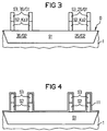
Figur 8- zeigt einen Ausschnitt aus einer Aufsicht auf das Substrat, in dem die erste Schichtstruktur, die zweite Schichtstruktur, die dritte Schichtstruktur, die vierte Schichtstruktur, der erste Bereich, der zweite Bereich, der dritte Bereich, der vierte Bereich, die erste Schicht, der erste Kontakt, der zweite Kontakt, der dritte Kontakt, der vierte Kontakt, der fünfte Kontakt, der sechste Kontakt, der siebte Kontakt, der achte Kontakt, die x-Achse und die y-Achse dargestellt sind.
- Figur 9
- zeigt eine Aufsicht auf das Substrat, in dem die Schichtstrukturen, die Kontakte, und die zweite Maske dargestellt sind.
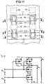
- Figur 10
- zeigt einen Ausschnitt aus einer Aufsicht auf das Substrat, in dem die Schichtstrukturen, die Kontakte, die fünften Bereiche und die vierte Fotolackmaske dargestellt sind.
Figur 11- zeigt einen Ausschnitt aus einer Aufsicht auf das Substrat, in dem die Schichtstrukturen, die Kontakte, die erste leitende Struktur und die zweite leitende Struktur dargestellt sind.
Figur 12- zeigt ein Schaltbild eines NAND-Gatters.
- Figure 1
- shows a first substrate after a first doped layer has been produced by implantation with the aid of a mask and a second layer, a third layer and a fourth layer have been grown epitaxially, a first auxiliary layer has been applied and structured, and on first edges and on second edges of the Auxiliary layer first spacers and second spacers were generated.
- Figure 2
- shows a cross section parallel to the cross section from FIG. 1 through the substrate after the first auxiliary layer has been removed, and a first layer structure, a second layer structure (not shown in this figure), a third layer structure (not shown in this figure) and a fourth layer structure were generated.
- Figure 3
- shows the cross section of Figure 1 after the process steps of Figure 2.
- Figure 4
- shows a cross section parallel to the cross section from FIG. 2 and FIG. 3 through the substrate after a first insulating structure and a second insulating structure have been produced.
- Figure 5
- shows the cross section of Figure 2 after the process steps of Figure 4.
- Figure 6
- 5 shows the cross section from FIG. 5 after the first insulating structure has been partially removed, a gate dielectric, a first gate electrode, a second gate electrode (not shown), a third gate electrode (not shown), a fourth gate electrode, a third insulating structure, a fourth insulating structure, a first contact, a second contact, a third contact, a fourth contact, a fifth contact, a sixth contact, a seventh contact, an eighth contact, a first conductive structure and a second conductive structure (not shown). The contacts are not all shown in this figure.
- Figure 7
- shows the cross section of Figure 4 after the process steps of Figure 6.
- Figure 8
- shows a section of a plan view of the substrate, in which the first layer structure, the second layer structure, the third layer structure, the fourth layer structure, the first region, the second region, the third region, the fourth region, the first layer, the first Contact, the second contact, the third contact, the fourth contact, the fifth contact, the sixth contact, the seventh contact, the eighth contact, the x-axis and the y-axis are shown.
- Figure 9
- shows a plan view of the substrate, in which the layer structures, the contacts, and the second mask are shown.
- Figure 10
- shows a section of a plan view of the substrate, in which the layer structures, the contacts, the fifth areas and the fourth photoresist mask are shown.
- Figure 11
- shows a section of a plan view of the substrate, in which the layer structures, the contacts, the first conductive structure and the second conductive structure are shown.
- Figure 12
- shows a circuit diagram of a NAND gate.
Die Figuren sind nicht maßstäblich.The figures are not to scale.
In einem ersten Ausführungsbeispiel wird mit Hilfe einer ersten
Fotolackmaske (nicht dargestellt), die einen l-förmigen
Bereich mit zusätzlichem Ausläufer nicht bedeckt, durch Implantation
eine ca.300nm dicke p-dotierte erste Schicht S1 in
einem Substrat 1 aus Silizium erzeugt. Die Dotierstoffkonzentration
der ersten Schicht beträgt ca. 1021 cm-3. Anschließend
wird an einer Oberfläche O des Substrats 1 durch epitaktisches
Aufwachsen eine n-dotierte zweite Schicht S2, eine p-dotierte
dritte Schicht S3 und eine n-dotierte vierte Schicht
S4 erzeugt. Die Dotierstoffkonzentrationen der zweiten
Schicht S2, der dritten Schicht S3 und der vierten Schicht S4
betragen jeweils ca. 1018 cm-3. Die zweite Schicht S2, die
dritte Schicht S3 und die vierte Schicht S4 sind jeweils ca.
200 nm dick. Anschließend wird die Dotierstoffkonzentration
der vierten Schicht S4 durch Implantation auf 1021cm-3 erhöht.
Durch Abscheiden von SiO2 in einer Dicke von ca. 200 nm
wird eine erste Hilfsschicht H1 erzeugt. Mit Hilfe einer
zweiten Fotolackmaske (nicht dargestellt), die einen ersten
länglichen rechteckigen Bereich B1 und einen dazu parallel
verlaufenden länglichen rechteckigen zweiten Bereich B2 nicht
bedeckt, wird SiO2 geätzt, bis die vierte Schicht S4 teilweise
freigelegt wird. Dadurch entstehen an Rändern des ersten
Bereichs B1 eine erste Kante Kn1 und an Rändern des zweiten
Bereichs B2 zweite Kanten Kn2. Der erste Bereich B1 und der
zweite Bereich B2 sind jeweils bezüglich einer zur Oberfläche
O parallel verlaufenden x-Achse x ca. 400 nm breit und bezüglich
einer zur Oberfläche O parallel verlaufenden und zur x-Achse
x senkrechten y-Achse y 2400 nm lang. Eine Verbindungslinie
zwischen einem Mittelpunkt des ersten Bereichs B1 und
einem Mittelpunkt des zweiten Bereichs B2 verläuft parallel
zur x-Achse (s. Fig. 8). Durch Abscheiden und Rückätzen von
Siliziumnitrid werden an der ersten Kante Kn1 erste Spacer
Sp1 und an der zweiten Kante Kn2 zweite Spacer Sp2 erzeugt
(siehe Figur 1).In a first exemplary embodiment, with the aid of a first photoresist mask (not shown), which does not cover an L-shaped region with an additional spur, an approximately 300 nm-thick p-doped first layer S1 is produced in a
Anschließend wird durch Ätzen mit z.B. NH4F/HF die strukturierte erste Hilfsschicht H1 entfernt. Um vier voneinander getrennte Schichtstrukturen zu erhalten, werden der erste Spacer Sp1 und der zweite Spacer Sp2 mit Hilfe einer dritten Fotolackmaske (nicht dargestellt), die einen den ersten Bereich B1 quer überlappenden rechteckigen dritten Bereich B3 und einen den zweiten Bereich B2 quer überlappenden rechteckigen vierten Bereich B4 nicht bedeckt, teilweise entfernt. Der strukturierte erste Spacer Sp1 und der strukturierte zweite Spacer Sp2 bilden zusammen eine erste Maske. Durch Ätzen von Silizium selektiv zu Siliziumnitrid mit z.B. HBr/NF3/He/O2 werden anschließend Teile der vierten Schicht S4 und der dritten Schicht S3 entfernt. Dadurch entstehen eine erste Schichtstruktur St1, eine vorläufige zweite Schichtstruktur, eine vorläufige dritte Schichtstruktur und eine vierte Schichtstruktur St4. Anschließend wird eine zweite Maske M2, die eine Hälfte des ersten Bereichs B1 und eine Hälfte des zweiten Bereichs B2 überlappt, erzeugt, indem SiO2 abgeschieden und durch ein fotolithographisches Verfahren strukturiert wird. Mit z.B. Cl2/CHF3 als Ätzmittel wird Silizium selektiv zu SiO2 geätzt, bis die zweite Schicht S2 an ungeschützten Stellen entfernt wird. Dadurch entstehen aus der vorläufigen zweiten Schichtstruktur und aus der vorläufigen dritten Schichtstruktur eine zweite Schichtstruktur St2 und eine dritte Schichtstruktur St3 (siehe Figur 2, Figur 3 und Figur 9). Die zweite Maske M2 ist über den ersten Bereich B1 hinaus teilweise lateral an die erste Schicht S1 angrenzend ausgedehnt, weswegen aus der ersten Schicht S1 und aus der zweiten Schicht S2 eine Stufe Stu gebildet wird (siehe Figur 9). Die zweite Maske M2 ist über den zweiten Bereich B2 hinaus ausgedehnt. Die durch die zweite Maske M2 außerhalb des ersten Bereichs B1 und des zweiten Bereichs B2 befindlichen geschützten Teile der zweiten Schicht S2 dienen als elektrische Verbindungen.The structured first auxiliary layer H1 is then removed by etching with, for example, NH 4 F / HF. In order to obtain four layer structures which are separate from one another, the first spacer Sp1 and the second spacer Sp2 are formed using a third photoresist mask (not shown) which has a rectangular third region B3 which overlaps the first region B1 and a rectangular fourth which overlaps the second region B2 Area B4 not covered, partially removed. The structured first spacer Sp1 and the structured second spacer Sp2 together form a first mask. Parts of the fourth layer S4 and the third layer S3 are subsequently removed by etching silicon selectively to silicon nitride with, for example, HBr / NF 3 / He / O 2 . This creates a first layer structure St1, a provisional second layer structure, a provisional third layer structure and a fourth layer structure St4. A second mask M2, which overlaps half of the first region B1 and half of the second region B2, is then produced by depositing SiO 2 and structuring it by means of a photolithographic process. Using, for example, Cl 2 / CHF 3 as an etchant, silicon is selectively etched to SiO 2 until the second layer S2 is removed at unprotected locations. As a result, a second layer structure St2 and a third layer structure St3 arise from the provisional second layer structure and from the provisional third layer structure (see FIG. 2, FIG. 3 and FIG. 9). The second mask M2 is partially extended laterally beyond the first region B1 to the first layer S1, which is why a step Stu is formed from the first layer S1 and the second layer S2 (see FIG. 9). The second mask M2 is extended beyond the second area B2. The protected parts of the second layer S2 which are located outside the first region B1 and the second region B2 through the second mask M2 serve as electrical connections.
Durch Implantation wird die Dotierstoffkonzentration der dritten Schicht S3 in der zweiten Schichtstruktur St2 und der dritten Schichtstruktur St3 auf ca. 1021cm-3 erhöht. Dazu wird die zweite Maske M2 beibehalten. Durch Ätzen mit z.B. HF wird die zweite Maske M2 anschließend entfernt.The implantation increases the dopant concentration of the third layer S3 in the second layer structure St2 and the third layer structure St3 to approximately 10 21 cm -3 . For this purpose, the second mask M2 is retained. The second mask M2 is subsequently removed by etching with, for example, HF.
Anschließend wird Siliziumnitrid in einer Dicke von ca. 80nm abgeschieden (siehe Figur 4). Durch Abscheiden und Strukturieren von SiO2 wird eine dritte Maske (nicht dargestellt) erzeugt, die fünfte Bereiche B5, in denen der erste Transistor, der zweite Transistor, der dritte Transistor und der vierte Transistor erzeugt werden, nicht bedeckt (s. Fig. 10). Anschließend wird mit z.B. CF4/CHF3/He Siliziumnitrid selektiv zu SiO2 und Silizium geätzt, wodurch eine erste isolierende Struktur I1 gebildet wird, die in den fünften Bereichen B5 spacerförmig und außerhalb der fünften Bereichen B5 konform ist (siehe Fig. 4 und Fig. 5). Anschließend wird durch thermische Oxidation mit geringem Temperaturbudget bei einer Temperatur von ca. 600°C und einem Druck von ca. 106Pa eine zweite isolierende Struktur I2 gebildet (siehe Figur 5). Anschließend wird Siliziumnitrid mit z.B. H3PO naß geätzt, und die dritte Maske durch nasses Ätzen mit z.B. HF entfernt. Durch thermische Oxidation wird ein Gatedielektrikum Gd aufgewachsen. Das Gatedielektrikum Gd entsteht an Stellen, an denen sich Teile der ersten isolierenden Struktur I1 innerhalb der fünften Bereiche B5 befanden.Silicon nitride is then deposited to a thickness of approximately 80 nm (see FIG. 4). By depositing and structuring SiO 2 , a third mask (not shown) is generated, the fifth regions B5, in which the first transistor, the second transistor, the third transistor and the fourth transistor are produced, are not covered (see FIG. 10 ). Subsequently, for example, CF 4 / CHF 3 / He silicon nitride is selectively etched to SiO 2 and silicon, whereby a first insulating structure I1 is formed, which is spacer-shaped in the fifth regions B5 and conforms outside the fifth regions B5 (see FIGS. 4 and Fig. 5). Subsequently, a second insulating structure I2 is formed by thermal oxidation with a low temperature budget at a temperature of approximately 600 ° C. and a pressure of approximately 10 6 Pa (see FIG. 5). Silicon nitride is then wet-etched with, for example, H 3 PO, and the third mask is removed by wet-etching with, for example, HF. A gate dielectric Gd is grown by thermal oxidation. The gate dielectric Gd is formed at locations where parts of the first insulating structure I1 were located within the fifth regions B5.
Anschließend wird in Situ dotiertes Polysilizium abgeschieden. Mit Hilfe einer vierten Fotolackmaske MF4, die den dritten Bereich B3 und den vierten Bereich B4 im wesentlichen bedeckt (s. Fig. 10), wird Polysilizium mit z.B. Cl2/CHF3 geätzt, wodurch an gegenüberliegenden Flanken der ersten Schichtstruktur St1 eine spacerförmige erste Gateelektrode Ga1, an gegenüberliegenden Flanken der zweiten Schichtstruktur St2 eine spacerförmige zweite Gateelektrode Ga2, an gegenüberliegenden Flanken der dritten Schichtstruktur St3 eine spacerförmige dritte Gateelektrode Ga3 und an gegenüberliegenden Flanken der vierten Schichtstruktur St4 eine spacerförmige vierte Gateelektrode Ga4 entstehen. Polysilizium unter der vierten Fotolackmaske MF4 dient als erste Kontaktfläche, die die dritte Gateelektrode Ga3 mit der vierten Gateelektrode Ga4 verbindet, und als zweite Kontaktfläche, die die erste Gateelektrode Ga1 mit der zweiten Gateelektrode Ga2 verbindet. Auf der ersten Kontaktfläche werden später ein erster Kontakt K1 und auf der zweiten Kontaktfläche ein zweiter Kontakt K2 erzeugt.Polysilicon doped in situ is then deposited. With the help of a fourth photoresist mask MF4, which essentially covers the third region B3 and the fourth region B4 (see FIG. 10), polysilicon is etched with, for example, Cl 2 / CHF 3 , as a result of which a spacer-shaped first is located on opposite flanks of the first layer structure St1 Gate electrode Ga1, a spacer-shaped second gate electrode Ga2 on opposite flanks of the second layer structure St2, a spacer-shaped third gate electrode Ga3 on opposite flanks of the third layer structure St3 and a spacer-shaped fourth gate electrode Ga4 are formed on opposite flanks of the fourth layer structure St4. Polysilicon under the fourth photoresist mask MF4 serves as the first contact area, which connects the third gate electrode Ga3 to the fourth gate electrode Ga4, and as the second contact area, which connects the first gate electrode Ga1 to the second gate electrode Ga2. A first contact K1 is created later on the first contact surface and a second contact K2 is generated on the second contact surface.
Die zweite isolierende Struktur I2 vermindert Kapazitäten, die durch die erste Gateelektrode Ga1 und der zweiten Schicht S2, durch die zweite Gateelektrode Ga2 und der ersten Schicht S1, durch die dritte Gateelektrode Ga3 und der ersten Schicht S1, und durch die vierte Gateelektrode Ga4 und der zweiten Schicht S2 gebildet werden.The second insulating structure I2 reduces capacities through the first gate electrode Ga1 and the second layer S2, through the second gate electrode Ga2 and the first layer S1, through the third gate electrode Ga3 and the first layer S1, and through the fourth gate electrode Ga4 and the second Layer S2 are formed.
Die Abmessungen des ersten Bereichs B1 und des zweiten Bereichs B2 wurden so gewählt, daß Polysilizium nach dem Ätzen diese Bereiche im wesentlichen bedeckt (siehe Figur 6).The dimensions of the first area B1 and the second area B2 were chosen so that polysilicon after etching these areas are essentially covered (see FIG. 6).
Anschließend wird SiO2 in einer Dicke von ca. 300 nm abgeschieden und mit z.B. Cl2/CHF3 rückgeätzt, wodurch eine dritte isolierende Struktur I3 erzeugt wird, die die erste Gateelektrode Ga1, die zweite Gateelektrode Ga2, die dritte Gateelektrode Ga3 und die vierte Gateelektrode Ga4, bedeckt. Anschließend wird Siliziumnitrid in einer Dicke von ca. 200 nm abgeschieden. Mit Hilfe einer fünften Fotolackmaske (nicht dargestellt) werden für Kontakte Vertiefungen erzeugt. Dabei wird mit z.B. CF4/CHF3/H2 Siliziumnitrid selektiv zu SiO2 geätzt. Die dritte isolierende Struktur I3 aus SiO2 dient als Ätzstop. Für den ersten Kontakt K1 wird eine Vertiefung bis zur ersten Kontaktfläche erzeugt. Für den zweiten Kontakt K2 wird eine Vertiefung bis zur zweiten Kontaktfläche erzeugt. Für einen dritten der Kontakte K3 wird eine Vertiefung erzeugt, die die Stufe Stu überlappt. Für einen vierten der Kontakte K4 wird in einer von der zweiten Maske M2 ursprünglich abgedeckten Stelle eine Vertiefung bis zu einem Teil der zweiten Schicht S2, der als elektrische Verbindung zum ersten Source/Drain-Gebiet des ersten Transistors dient, erzeugt. Für einen fünften der Kontakte K5 wird eine Vertiefung bis zum ersten Source/Drain-Gebiets des dritten Transistors erzeugt. Für einen sechsten der Kontakte K6 wird eine Vertiefung bis zum ersten Source/Drain-Gebiets des zweiten Transistors erzeugt. Für einen siebten der Kontakte K7 wird eine Vertiefung bis zum ersten Source/Drain-Gebiets des vierten Transistors erzeugt. Für einen achten der Kontakte K8 wird eine Vertiefung bis zum zweiten Source/Drain-Gebiets des ersten Transistors erzeugt.Subsequently, SiO 2 is deposited in a thickness of approx. 300 nm and etched back with, for example, Cl 2 / CHF 3 , whereby a third insulating structure I3 is generated, which comprises the first gate electrode Ga1, the second gate electrode Ga2, the third gate electrode Ga3 and the fourth Gate electrode Ga4, covered. Silicon nitride is then deposited to a thickness of approximately 200 nm. With the help of a fifth photoresist mask (not shown), depressions are created for contacts. CF 4 / CHF 3 / H 2 silicon nitride is selectively etched to SiO 2 . The third insulating structure I3 made of SiO 2 serves as an etch stop. A depression up to the first contact surface is produced for the first contact K1. A depression up to the second contact surface is produced for the second contact K2. For a third of the contacts K3, a recess is created which overlaps the Stu step. For a fourth of the contacts K4, a depression up to a part of the second layer S2, which serves as an electrical connection to the first source / drain region of the first transistor, is produced in a location originally covered by the second mask M2. A depression up to the first source / drain region of the third transistor is produced for a fifth of the contacts K5. A depression up to the first source / drain region of the second transistor is produced for a sixth of the contacts K6. A depression up to the first source / drain region of the fourth transistor is produced for a seventh of the contacts K7. For an eighth of the contacts K8, a depression is produced up to the second source / drain region of the first transistor.
In einer Dicke von ca. 100nm wird Titan abgeschieden und selektiv siliziert, wodurch Kontaktstrukturen Ks entstehen. Übrigbleibendes Titan wird mit z.B. CCl2F2/NF3 entfernt.Titanium is deposited in a thickness of approx. 100 nm and selectively siliconized, which creates contact structures Ks. Remaining titanium is removed with, for example, CCl 2 F 2 / NF 3 .
In einer Dicke von ca. 400 nm wird Aluminium abgeschieden, wodurch die Kontakte K1, K2, K3, K4, K5, K6, K7, K8 entstehen. Anschließend wird das Aluminium so strukturiert, daß eine erste leitende Struktur L1 erzeugt wird, die den siebten Kontakt K7 und den achten Kontakt K8 miteinander verbindet und eine zweite leitende Struktur L2 erzeugt wird, die den fünften Kontakt K5 und den sechsten Kontakt K6 miteinander verbindet (siehe Figur 6). Die Kontaktstrukturen Ks verringern die elektrischen Widerstände der Kontakte K1, K2, K3, K4, K5, K6, K7, K8.Aluminum is deposited in a thickness of approx. 400 nm, which creates the contacts K1, K2, K3, K4, K5, K6, K7, K8. The aluminum is then structured so that a first conductive structure L1 is generated, the seventh Contact K7 and the eighth contact K8 connects to each other and a second conductive structure L2 is created which corresponds to the fifth contact K5 and sixth contact K6 with each other connects (see Figure 6). Reduce the contact structures Ks the electrical resistances of contacts K1, K2, K3, K4, K5, K6, K7, K8.
Die vier Transistoren bilden ein NAND-Gatter (siehe Figur 12). Der erste Kontakt K1 wird mit einem ersten Eingangsspannungsanschluß UIN1 verbunden. Der zweite Kontakt K2 wird mit einem zweiten Eingangsspannungsanschluß UIN2 verbunden. Der dritte Kontakt K3 wird mit einem Ausgangsspannungsanschluß UOUT verbunden. Der vierte Kontakt K4 wird mit einem ersten Spannungsanschluß USS verbunden. Die zweite leitende Struktur L2 wird mit einem zweiten Spannungsanschluß UDD verbunden.The four transistors form a NAND gate (see Figure 12). The first contact K1 is connected to a first input voltage connection U IN1 . The second contact K2 is connected to a second input voltage connection U IN2 . The third contact K3 is connected to an output voltage connection U OUT . The fourth contact K4 is connected to a first voltage connection U SS . The second conductive structure L2 is connected to a second voltage connection U DD .
Es sind viele Variationen des Ausführungsbeispiels denkbar, die ebenfalls im Rahmen der Erfindung liegen. Insbesondere können die Abmessungen der beschriebenen Schichten, Gebiete, Bereiche und Strukturen an die jeweiligen Erfordernisse angepaßt werden. Dasselbe gilt auch für die vorgeschlagenen Dotierstoffkonzentrationen. Die zweite isolierende Struktur kann auch durch ein Abscheidungsverfahren erzeugt werden. Many variations of the exemplary embodiment are conceivable, which are also within the scope of the invention. Especially the dimensions of the layers, areas, Areas and structures adapted to the respective requirements become. The same applies to the proposed dopant concentrations. The second isolating structure can also be generated by a deposition process.
Isolierende Strukturen können auch aus anderen isolierenden Materialien erzeugt werden. Statt dotiertem Polysilizium lassen sich auch z.B. Metallsilizide und/oder Metalle verwenden.Insulating structures can also be made from other insulating ones Materials are created. Leave instead of doped polysilicon also e.g. Use metal silicides and / or metals.
Claims (9)
Applications Claiming Priority (2)
| Application Number | Priority Date | Filing Date | Title |
|---|---|---|---|
| DE19736672 | 1997-08-22 | ||
| DE19736672 | 1997-08-22 |
Publications (3)
| Publication Number | Publication Date |
|---|---|
| EP0899783A2 true EP0899783A2 (en) | 1999-03-03 |
| EP0899783A3 EP0899783A3 (en) | 2000-08-16 |
| EP0899783B1 EP0899783B1 (en) | 2008-04-16 |
Family
ID=7839912
Family Applications (1)
| Application Number | Title | Priority Date | Filing Date |
|---|---|---|---|
| EP98115375A Expired - Lifetime EP0899783B1 (en) | 1997-08-22 | 1998-08-14 | Circuit arrangement with at least four transistors and method of fabrication |
Country Status (6)
| Country | Link |
|---|---|
| US (1) | US6060911A (en) |
| EP (1) | EP0899783B1 (en) |
| JP (1) | JPH11145309A (en) |
| KR (1) | KR100547400B1 (en) |
| DE (1) | DE59814218D1 (en) |
| TW (1) | TW423116B (en) |
Cited By (2)
| Publication number | Priority date | Publication date | Assignee | Title |
|---|---|---|---|---|
| WO2000046855A1 (en) * | 1999-02-03 | 2000-08-10 | France Telecom | Semiconductor device of nand and nor logic gates with n inputs and method for making same |
| EP1063697A1 (en) * | 1999-06-18 | 2000-12-27 | Lucent Technologies Inc. | A cmos integrated circuit having vertical transistors and a process for fabricating same |
Families Citing this family (4)
| Publication number | Priority date | Publication date | Assignee | Title |
|---|---|---|---|---|
| EP0996982B1 (en) * | 1997-07-18 | 2008-10-29 | Infineon Technologies AG | Method for making a vertical mos transistor |
| JP2007220808A (en) * | 2006-02-15 | 2007-08-30 | Toshiba Corp | Semiconductor device and its manufacturing method |
| US7838948B2 (en) * | 2007-01-30 | 2010-11-23 | Infineon Technologies Ag | Fin interconnects for multigate FET circuit blocks |
| JP5635256B2 (en) | 2009-11-24 | 2014-12-03 | ピーエスフォー ルクスコ エスエイアールエルPS4 Luxco S.a.r.l. | Semiconductor device and manufacturing method thereof |
Citations (6)
| Publication number | Priority date | Publication date | Assignee | Title |
|---|---|---|---|---|
| DE3838355A1 (en) * | 1988-11-11 | 1990-05-17 | Fraunhofer Ges Forschung | Vertical transistor arrangement |
| US5032529A (en) * | 1988-08-24 | 1991-07-16 | Harris Corporation | Trench gate VCMOS method of manufacture |
| EP0657930A2 (en) * | 1993-12-07 | 1995-06-14 | Siemens Aktiengesellschaft | Integrated circuit structure with at least a CMOS NAND gate and method of fabricating the same |
| EP0721221A2 (en) * | 1995-01-03 | 1996-07-10 | International Business Machines Corporation | FET and/or bipolar devices formed in thin vertical silicon on insulator (SOI) structures |
| US5612563A (en) * | 1992-03-02 | 1997-03-18 | Motorola Inc. | Vertically stacked vertical transistors used to form vertical logic gate structures |
| US5627395A (en) * | 1992-09-02 | 1997-05-06 | Motorola Inc. | Vertical transistor structure |
Family Cites Families (8)
| Publication number | Priority date | Publication date | Assignee | Title |
|---|---|---|---|---|
| US4951102A (en) * | 1988-08-24 | 1990-08-21 | Harris Corporation | Trench gate VCMOS |
| JP2991489B2 (en) * | 1990-11-30 | 1999-12-20 | 株式会社東芝 | Semiconductor device |
| US5252849A (en) * | 1992-03-02 | 1993-10-12 | Motorola, Inc. | Transistor useful for further vertical integration and method of formation |
| US5208172A (en) * | 1992-03-02 | 1993-05-04 | Motorola, Inc. | Method for forming a raised vertical transistor |
| US5324673A (en) * | 1992-11-19 | 1994-06-28 | Motorola, Inc. | Method of formation of vertical transistor |
| KR100193102B1 (en) * | 1994-08-25 | 1999-06-15 | 무명씨 | Semiconductor device and manufacturing method thereof |
| US5872374A (en) * | 1996-03-29 | 1999-02-16 | Motorola, Inc. | Vertical semiconductor device |
| US5923185A (en) * | 1997-03-12 | 1999-07-13 | Xilinx, Inc. | Logic circuit programmable to implement at least two logic functions |
-
1998
- 1998-08-03 TW TW087112741A patent/TW423116B/en not_active IP Right Cessation
- 1998-08-14 EP EP98115375A patent/EP0899783B1/en not_active Expired - Lifetime
- 1998-08-14 DE DE59814218T patent/DE59814218D1/en not_active Expired - Lifetime
- 1998-08-19 JP JP23314198A patent/JPH11145309A/en not_active Withdrawn
- 1998-08-21 US US09/138,160 patent/US6060911A/en not_active Expired - Lifetime
- 1998-08-21 KR KR1019980033909A patent/KR100547400B1/en not_active IP Right Cessation
Patent Citations (6)
| Publication number | Priority date | Publication date | Assignee | Title |
|---|---|---|---|---|
| US5032529A (en) * | 1988-08-24 | 1991-07-16 | Harris Corporation | Trench gate VCMOS method of manufacture |
| DE3838355A1 (en) * | 1988-11-11 | 1990-05-17 | Fraunhofer Ges Forschung | Vertical transistor arrangement |
| US5612563A (en) * | 1992-03-02 | 1997-03-18 | Motorola Inc. | Vertically stacked vertical transistors used to form vertical logic gate structures |
| US5627395A (en) * | 1992-09-02 | 1997-05-06 | Motorola Inc. | Vertical transistor structure |
| EP0657930A2 (en) * | 1993-12-07 | 1995-06-14 | Siemens Aktiengesellschaft | Integrated circuit structure with at least a CMOS NAND gate and method of fabricating the same |
| EP0721221A2 (en) * | 1995-01-03 | 1996-07-10 | International Business Machines Corporation | FET and/or bipolar devices formed in thin vertical silicon on insulator (SOI) structures |
Cited By (2)
| Publication number | Priority date | Publication date | Assignee | Title |
|---|---|---|---|---|
| WO2000046855A1 (en) * | 1999-02-03 | 2000-08-10 | France Telecom | Semiconductor device of nand and nor logic gates with n inputs and method for making same |
| EP1063697A1 (en) * | 1999-06-18 | 2000-12-27 | Lucent Technologies Inc. | A cmos integrated circuit having vertical transistors and a process for fabricating same |
Also Published As
| Publication number | Publication date |
|---|---|
| EP0899783A3 (en) | 2000-08-16 |
| KR19990023755A (en) | 1999-03-25 |
| JPH11145309A (en) | 1999-05-28 |
| TW423116B (en) | 2001-02-21 |
| US6060911A (en) | 2000-05-09 |
| DE59814218D1 (en) | 2008-05-29 |
| KR100547400B1 (en) | 2006-03-23 |
| EP0899783B1 (en) | 2008-04-16 |
Similar Documents
| Publication | Publication Date | Title |
|---|---|---|
| DE10141916A1 (en) | MOS semiconductor device and method of manufacturing the same | |
| EP0101000B1 (en) | Integrated semiconductor circuit, comprising bipolar and mos transistors on the same chip, and method of making the same | |
| DE102012214077A1 (en) | Integrated circuits with protruding source and drain regions and method for forming integrated circuits | |
| DE3110477A1 (en) | METHOD FOR PRODUCING CMOS COMPONENTS | |
| DE4224793A1 (en) | THIN FILM FIELD EFFECT ELEMENT AND PRODUCTION METHOD DAFUER | |
| DE19501557A1 (en) | Semiconductor device and method for its production | |
| DE19853268C2 (en) | Field effect controlled transistor and method for its production | |
| DE10107012A1 (en) | Simultaneous formation of poly-poly capacitor, MOS transistor and bipolar transistor on substrate used in production of integrated circuits comprises using polycrystalline silicon to form electrodes | |
| DE69738558T2 (en) | Method for producing a transistor with self-aligning contacts | |
| DE112006001520B4 (en) | Process for making raised source and drain regions with spacers to be removed, avoiding "mouse ears" | |
| DE19720193C2 (en) | Integrated circuit arrangement with at least two vertical MOS transistors and method for their production | |
| DE112016000050T5 (en) | Method for producing a split-gate power component | |
| EP1129482A1 (en) | Method for producing a DRAM Cell System | |
| EP0920060B1 (en) | SRAM cell array and fabrication process thereof | |
| EP0899783B1 (en) | Circuit arrangement with at least four transistors and method of fabrication | |
| DE3119137A1 (en) | SEMICONDUCTOR AND METHOD FOR THE PRODUCTION THEREOF | |
| DE19746900C2 (en) | Vertical MOS transistor and method for its production | |
| DE2738049A1 (en) | INTEGRATED SEMI-CONDUCTOR CIRCUIT ARRANGEMENT | |
| DE19845066C2 (en) | Integrated circuit arrangement and method for its production | |
| DE19836953B4 (en) | MOSFET and method for its production | |
| EP0996982B1 (en) | Method for making a vertical mos transistor | |
| DE2806410A1 (en) | CONDUCTOR ARRANGEMENT AND METHOD OF MANUFACTURING IT | |
| EP0756321A1 (en) | Process for manufacturing complementary MOS transistors | |
| DE102017110440A1 (en) | Improved PMOS Finfet | |
| DE19957303B4 (en) | MOS transistor and method for its production |
Legal Events
| Date | Code | Title | Description |
|---|---|---|---|
| PUAI | Public reference made under article 153(3) epc to a published international application that has entered the european phase |
Free format text: ORIGINAL CODE: 0009012 |
|
| AK | Designated contracting states |
Kind code of ref document: A2 Designated state(s): DE FR GB IT |
|
| AX | Request for extension of the european patent |
Free format text: AL;LT;LV;MK;RO;SI |
|
| PUAL | Search report despatched |
Free format text: ORIGINAL CODE: 0009013 |
|
| AK | Designated contracting states |
Kind code of ref document: A3 Designated state(s): AT BE CH CY DE DK ES FI FR GB GR IE IT LI LU MC NL PT SE |
|
| AX | Request for extension of the european patent |
Free format text: AL;LT;LV;MK;RO;SI |
|
| 17P | Request for examination filed |
Effective date: 20000904 |
|
| AKX | Designation fees paid |
Free format text: DE FR GB IT |
|
| RAP1 | Party data changed (applicant data changed or rights of an application transferred) |
Owner name: INFINEON TECHNOLOGIES AG |
|
| 17Q | First examination report despatched |
Effective date: 20060721 |
|
| GRAP | Despatch of communication of intention to grant a patent |
Free format text: ORIGINAL CODE: EPIDOSNIGR1 |
|
| RAP1 | Party data changed (applicant data changed or rights of an application transferred) |
Owner name: QIMONDA AG |
|
| GRAS | Grant fee paid |
Free format text: ORIGINAL CODE: EPIDOSNIGR3 |
|
| GRAA | (expected) grant |
Free format text: ORIGINAL CODE: 0009210 |
|
| AK | Designated contracting states |
Kind code of ref document: B1 Designated state(s): DE FR GB IT |
|
| REF | Corresponds to: |
Ref document number: 59814218 Country of ref document: DE Date of ref document: 20080529 Kind code of ref document: P |
|
| PLBE | No opposition filed within time limit |
Free format text: ORIGINAL CODE: 0009261 |
|
| STAA | Information on the status of an ep patent application or granted ep patent |
Free format text: STATUS: NO OPPOSITION FILED WITHIN TIME LIMIT |
|
| EN | Fr: translation not filed | ||
| 26N | No opposition filed |
Effective date: 20090119 |
|
| GBPC | Gb: european patent ceased through non-payment of renewal fee |
Effective date: 20080814 |
|
| PG25 | Lapsed in a contracting state [announced via postgrant information from national office to epo] |
Ref country code: IT Free format text: LAPSE BECAUSE OF FAILURE TO SUBMIT A TRANSLATION OF THE DESCRIPTION OR TO PAY THE FEE WITHIN THE PRESCRIBED TIME-LIMIT Effective date: 20080416 |
|
| PG25 | Lapsed in a contracting state [announced via postgrant information from national office to epo] |
Ref country code: GB Free format text: LAPSE BECAUSE OF NON-PAYMENT OF DUE FEES Effective date: 20080814 |
|
| PG25 | Lapsed in a contracting state [announced via postgrant information from national office to epo] |
Ref country code: FR Free format text: LAPSE BECAUSE OF FAILURE TO SUBMIT A TRANSLATION OF THE DESCRIPTION OR TO PAY THE FEE WITHIN THE PRESCRIBED TIME-LIMIT Effective date: 20090227 |
|
| REG | Reference to a national code |
Ref country code: DE Ref legal event code: R081 Ref document number: 59814218 Country of ref document: DE Owner name: POLARIS INNOVATIONS LTD., IE Free format text: FORMER OWNER: QIMONDA AG, 81739 MUENCHEN, DE Ref country code: DE Ref legal event code: R081 Ref document number: 59814218 Country of ref document: DE Owner name: INFINEON TECHNOLOGIES AG, DE Free format text: FORMER OWNER: QIMONDA AG, 81739 MUENCHEN, DE |
|
| REG | Reference to a national code |
Ref country code: DE Ref legal event code: R081 Ref document number: 59814218 Country of ref document: DE Owner name: POLARIS INNOVATIONS LTD., IE Free format text: FORMER OWNER: INFINEON TECHNOLOGIES AG, 85579 NEUBIBERG, DE |
|
| PGFP | Annual fee paid to national office [announced via postgrant information from national office to epo] |
Ref country code: DE Payment date: 20150929 Year of fee payment: 18 |
|
| REG | Reference to a national code |
Ref country code: DE Ref legal event code: R119 Ref document number: 59814218 Country of ref document: DE |
|
| PG25 | Lapsed in a contracting state [announced via postgrant information from national office to epo] |
Ref country code: DE Free format text: LAPSE BECAUSE OF NON-PAYMENT OF DUE FEES Effective date: 20170301 |