EP0899108A2 - Ink jet printhead and heater chip - Google Patents
Ink jet printhead and heater chip Download PDFInfo
- Publication number
- EP0899108A2 EP0899108A2 EP98305292A EP98305292A EP0899108A2 EP 0899108 A2 EP0899108 A2 EP 0899108A2 EP 98305292 A EP98305292 A EP 98305292A EP 98305292 A EP98305292 A EP 98305292A EP 0899108 A2 EP0899108 A2 EP 0899108A2
- Authority
- EP
- European Patent Office
- Prior art keywords
- conductor
- dielectric layer
- heating element
- conductors
- set forth
- Prior art date
- Legal status (The legal status is an assumption and is not a legal conclusion. Google has not performed a legal analysis and makes no representation as to the accuracy of the status listed.)
- Withdrawn
Links
Images


Classifications
-
- B—PERFORMING OPERATIONS; TRANSPORTING
- B41—PRINTING; LINING MACHINES; TYPEWRITERS; STAMPS
- B41J—TYPEWRITERS; SELECTIVE PRINTING MECHANISMS, i.e. MECHANISMS PRINTING OTHERWISE THAN FROM A FORME; CORRECTION OF TYPOGRAPHICAL ERRORS
- B41J2/00—Typewriters or selective printing mechanisms characterised by the printing or marking process for which they are designed
- B41J2/005—Typewriters or selective printing mechanisms characterised by the printing or marking process for which they are designed characterised by bringing liquid or particles selectively into contact with a printing material
- B41J2/01—Ink jet
- B41J2/135—Nozzles
- B41J2/14—Structure thereof only for on-demand ink jet heads
- B41J2/14016—Structure of bubble jet print heads
- B41J2/14088—Structure of heating means
- B41J2/14112—Resistive element
- B41J2/14129—Layer structure
-
- B—PERFORMING OPERATIONS; TRANSPORTING
- B41—PRINTING; LINING MACHINES; TYPEWRITERS; STAMPS
- B41J—TYPEWRITERS; SELECTIVE PRINTING MECHANISMS, i.e. MECHANISMS PRINTING OTHERWISE THAN FROM A FORME; CORRECTION OF TYPOGRAPHICAL ERRORS
- B41J2/00—Typewriters or selective printing mechanisms characterised by the printing or marking process for which they are designed
- B41J2/005—Typewriters or selective printing mechanisms characterised by the printing or marking process for which they are designed characterised by bringing liquid or particles selectively into contact with a printing material
- B41J2/01—Ink jet
- B41J2/135—Nozzles
- B41J2/14—Structure thereof only for on-demand ink jet heads
- B41J2/14016—Structure of bubble jet print heads
- B41J2/14072—Electrical connections, e.g. details on electrodes, connecting the chip to the outside...
Definitions
- This invention relates to ink jet printheads and heater chips having heating elements and conductors for delivering energy to the heating elements.
- Drop-on-demand ink jet printers use thermal energy to produce a vapor bubble in an ink-filled chamber to expel a droplet.
- a thermal energy generator or heating element usually a resistor, is located in the chamber on a heater chip near a discharge orifice.
- a plurality of chambers, each provided with a single heating element, are provided in the printer's printhead.
- the printhead typically comprises the heater chip and a plate having a plurality of the discharge orifices formed therein.
- the printhead forms part of an ink jet print cartridge which further comprises an ink-filled container.
- the resistors are individually addressed with an energy pulse to momentarily vaporize the ink and form a bubble which expels an ink droplet.
- a flexible circuit may be used to provide a path for energy pulses to travel from a printer energy supply circuit to the printhead. Bond pads on the printhead are coupled to end sections of traces on the circuit. A plurality of first and second conductors are provided on the heater chip and extend between the bond pads and the resistors. Current is delivered to the resistors via the traces, the bond pads and the first and second conductors.
- first generation printheads the number of first conductors and associated bond pads equaled the number of resistors provided on the chip. However, fewer second conductors, each coupled to two or more resistors, were provided. The first and second conductors were located in generally the same plane as the resistors.
- Decoder circuitry In order to reduce the number of first conductors and associated bond pads, later printers and printheads were provided with decoder circuitry. Decoder circuitry, however, is expensive and, hence, undesirable.
- an ink jet printhead having a heater chip including a plurality of first and second conductors arranged in spaced-apart planes and/or in a matrix.
- first and second conductors are required on the heater chip.
- decoder circuitry is substantially reduced or completely eliminated.
- the first and second conductors are vertically spaced apart, fewer conductors are located in substantially the same plane as the heating elements. Hence, a higher density of heating elements may be provided on the heater chip.
- the heating elements are located on a thermally non-conductive layer. For this reason, it is believed that the heater chip of this embodiment has improved thermal efficiency and, hence, requires less energy to effect bubble formation than conventional heater chips.
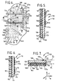
- a heater chip 10, formed in accordance with a first embodiment of the present invention, is illustrated in Figs. 1-3.
- An orifice plate 30 is adapted to be secured to the chip 10 via an adhesive 40, see Fig. 3.
- the coupled chip 10 and plate 30 define an ink jet printhead which is secured to an ink-filled often polymeric container (not shown).
- the joined polymeric container and printhead form a portion of an ink jet print cartridge which is adapted to be installed in an ink jet printer (not shown).
- the polymeric container may be capable of being refilled with ink.
- the heater chip 10 is provided with a plurality of T-shaped resistive heating element sections 11a-11d. As will be discussed more explicitly below, portions of the heating element sections 11a-11d define resistive heating elements 12. While the heating elements 12 in the embodiment illustrated in Figs. 1-3 comprise portions of the heating element sections 11a-11d, the heating elements 12 are designated in Figs. 1 and 2 by squares shown in dotted line to allow for ease in understanding the present invention.
- the plate 30 includes openings 32 which extend completely through the plate 30 and define orifices 32a through which ink droplets are ejected.
- Sections 34 of the plate 30 and portions 14 of the heater chip 10 define a plurality of bubble chambers 50.
- the resistive heating element sections 11a-11d are located on the chip 10 such that a portion of a heating element section 11a-11d, i.e., a single heating element 12, is associated with each of the bubble chambers 50, see Fig. 3.
- Ink supplied by the polymeric container flows into a central opening 15 formed in the chip 10. The ink then moves through ink supply channels 52 into the bubble chambers 50.
- the resistive heating elements 12 are individually addressed by energy pulses. Each energy pulse is applied to a heating element 12 to momentarily vaporize the ink in the bubble chamber 50 with which the heating element 12 is associated to form a bubble within the chamber 50. The function of the bubble is to displace ink within the chamber 50 such that a droplet of ink is expelled through the bubble chamber orifice 32a.
- a flexible circuit (not shown) secured to the polymeric container is used to provide a path for energy pulses to travel from a printer energy supply circuit to the heater chip 10. Bond pads 16, see Fig. 1, on the heater chip 10 are bonded to end sections of traces (not shown) on the flexible circuit. Current flows from the printer energy supply circuit to the traces on the flexible circuit and from the traces to the bond pads 16 on the heater chip 10.
- the heater chip 10 comprises a main body portion 18 including a plurality of first and second conductors.
- first and second sets 80a and 80b of six first conductors 60a-60f, four second conductors 70a-70d, and four heating element sections 11a-11d are shown on opposite sides of the central opening 15.
- Each heating element section 11a-11d defines six heating elements 12 such that four heating element sections 11a-11d provide 24 heating elements 12.
- the eight heating element sections 11a-11d provide 48 heating elements 12.
- the first and second conductors 60a-60f and 70a-70d in each of the first and second sets 80a and 80b are arranged in a matrix having first conductor rows and second conductor columns.
- Each second conductor column is defined by a single second conductor 70a-70d such that four columns are provided which are positioned in-line with one another. Hence, only six first conductors 60a-60f and four second conductors 70a-70d are required to effect the firing of 24 heating elements 12. It is contemplated by the present invention that the number of heating elements 12 and the number of first and second conductors 60 and 70 provided on the chip 10 may be varied.
- each of the first conductors 60a-60f comprises one primary conductor 62 and four secondary conductors 68.
- the primary conductor 62 has first and second segments 64 and 66.
- the first end 64a of the first segment 64 is coupled to a bond pad 16.
- the second end 64b of the first segment 64 is coupled to a second segment 66.
- the second segment 66 is coupled to four secondary conductors 68 at spaced-apart points 66b along its length.
- Each of the four secondary conductors 68 to which a given second segment 66 is coupled extends below and is positioned in-line with a different one of the four second conductors 70a-70d, see Figs. 1-3.
- each of the four second conductors 70a-70d is positioned above and is located in-line with a single secondary conductor 68 of each of the first conductors 60a-60f.
- Each of the second conductors 70a-70d comprises a first segment 72 and a second segment 74 which is substantially transverse to the first segment 72.
- a first end 72a of the first segment 72 is coupled to a bond pad 16 while a second end 72b of the first segment 72 is coupled to the second segment 74 at an intermediate point along the second segment 74.
- Each second segment 74 extends over and contacts six heating elements 12.
- heating element 12 In order to effect the firing of a given heating element 12, current is passed through the first conductor 60a-60f which is positioned directly below the heating element 12 and the second conductor 70a-70d which is positioned above and contacts the heating element 12.
- heating element 12a in Fig. 1 is fired by passing current through the first conductor 60b and the second conductor 70b.
- Heating element 12b is fired by passing current through the first conductor 60a and the second conductor 70d.
- the main body portion 18 further includes a base portion 90 and a first dielectric layer 92 formed over the base portion 90.
- the base portion 90 may be formed from silicon, i.e., it may comprise a silicon wafer section. Alternatively, the base portion 90 may be formed from any other substrate material which is substantially ink resistant, such as alumina or stainless steel.
- the dielectric layer 92 may be formed from any commercially available dielectric material, such as silicon dioxide or silicon nitride.
- the base portion 90 preferably has a thickness of from about 400 ⁇ m to about 800 ⁇ m, as measured in the Z-direction, see Fig. 3.
- the dielectric layer 92 preferably has a thickness of from about 0.1 ⁇ m to about 5.0 ⁇ m. If the dielectric layer 92 is formed from silicon dioxide, it may be formed via a conventional thermal oxidation, sputtering or chemical vapor deposition process. If the dielectric layer 92 is formed from silicon nitride, it may be formed via a sputtering or chemical vapor deposition process.
- the primary conductors 62 are formed on the dielectric layer 92.
- Aluminum or any other highly conductive material such as copper or gold, may be employed.
- a layer of aluminum may be added to the dielectric layer 92 via a conventional vacuum evaporation process.
- a conventional sputter deposition process may be employed.
- a conventional photomasking process is then used to remove unwanted metal such that the remaining metal defines the primary conductors 62.
- a conventional lift-off photolithography process may be used to remove the unwanted metal.
- the lift-off process involves forming a photoresist layer (also referred to herein as a resist layer) on the dielectric layer 92 before adding the aluminum material.
- the conductors 62 preferably have a thickness of from about 0.2 ⁇ m to about 2 ⁇ m, as measured in the Z-direction, see Fig. 3.
- the first segments 64 preferably have a width of from about 10 ⁇ m to about 100 ⁇ m, as measured in the Y-direction, and the second segments 66 preferably have a width of from about 10 ⁇ m to about 100 ⁇ m, as measured in the X-direction.
- a second dielectric layer 96 is formed over the exposed portions of the dielectric layer 92 and the conductors 62.
- the layer 96 is preferably formed from any one of a number of commercially available polymeric photoresist materials.
- An example of such a material is a negative acting photoresist material, which is commercially available from Shipley Company Inc. under the product name "MEGAPOSIT SNRTM 248 PHOTO RESIST.”
- the dielectric layer 96 extends into areas between the conductors 62 so as to prevent current movement between adjacent conductors 62.
- the layer 96 also covers the conductors 62 except at the points 66b where the second segments 66 of the conductors 62 are to be coupled to the secondary conductors 68, see Fig. 3.
- a conventional material removal process is used to remove portions of the dielectric layer 96 located above the points 66b so as to form openings 96a in the layer 96.
- the dielectric layer 96 at locations not covering the conductors 62, preferably has a thickness of from about 1 ⁇ m to about 5 ⁇ m, as measured in the Z-direction, see Fig. 3.
- the secondary conductors 68 are added to the dielectric layer 96 such that they are positioned in a first horizontal plane P 1 , see Fig. 3.
- the conductors 68 are preferably formed from aluminum or a like material via a conventional vacuum evaporation process and a photomasking process. Alternatively, the conductors 68 may be formed via a conventional sputter deposition process and/or a lift-off photolithography process.
- the aluminum material extends through the openings 96a in the dielectric layer 96.
- the secondary conductors 68 extend through the openings 96a in the layer 96 and engage the second segments 66 of the conductors 62 at points 66b.
- the conductors 68 preferably have a thickness of from about 0.2 ⁇ m to about 2 ⁇ m, as measured in the Z-direction, and a width of from about 10 ⁇ m to about 100 ⁇ m, as measured in the Y-direction, see Fig. 3.
- a third dielectric layer 98 is added over the exposed portions of the dielectric layer 96 and the conductors 68.
- the layer 98 preferably comprises the same material from which the dielectric layer 96 is formed.
- the layer 98 extends into areas between the conductors 68 so as to prevent current movement between adjacent conductors 68.
- the layer 98 also extends over the conductors 68.
- a conventional material removal process a development process in the illustrated embodiment, is used to form openings 98a in the dielectric layer 98 located above end regions 68a of the conductors 68, which regions 68a are positioned in-line with the heating elements 12, see Fig. 3.
- the openings 98a may be square in shape having a length along each side which is from about 15 microns to about 50 microns and preferably about 30 microns.
- the openings 98a may also be circular, elliptical, annular or rectangular in shape. If the openings 98a are square or rectangular, they may have rounded corners.
- the dielectric layer 98, at regions not positioned over a conductor 68, preferably has a thickness of from about 1 ⁇ m to about 5 ⁇ m, as measured in the Z-direction, see Fig. 3.
- a current transfer layer 100 is added to the dielectric layer 98. It extends through the openings 98a in the dielectric layer 98 so as to engage the end regions 68a of the conductors 68.
- the material from which the layer 100 is formed is electrically conductive so as to allow current to flow between the first conductors 60a-60f and the heating elements 12. The material, however, should not be so conductive as to allow current to flow substantially into a neighboring heating element 12.
- the resistivity of the material is preferably from about 0.1 W-cm to about 5 W-cm, and more preferably about 1 W-cm.
- the material be temperature resistant if heated to a temperature of less than about 350°C for about 5 mseconds. It is further preferred that the material be thermally non-conductive.
- the thermal conductivity of the material is preferably from about 0.1 W/m°C to about 15 W/m°C, and more preferably from about 0.1 W/m°C to about 0.5 W/m°C.
- the material is a high temperature resistant polymer loaded with an electrically conductive filler.
- An example of such a material is a carbon-filled polyimide material.
- Such a material may be formed by blending a commercially available polyimide material with a carbon black material such that the latter is generally evenly dispersed throughout the polyimide material.
- the current transfer layer 100 may be formed via a conventional spin application process followed by a conventional oven curing process.
- the layer 100 preferably has a thickness of from about 5 ⁇ m to about 50 ⁇ m, as measured in the Z-direction, see Fig. 3.
- the heating element sections 11a-11d are formed on the current transfer layer 100, see Fig. 3.
- the resistive material from which the heating element sections 11a-11d are formed preferably comprises TaO x .
- X is ⁇ 2 and preferably ⁇ 1, thus indicating a substantially non-stoichiometric condition.
- This material may be deposited via a reactive sputtering process. During that process, oxygen gas along with an inert working gas is added to a vacuum chamber. The oxygen gas reacts with the tantalum vapor material in the chamber so as to deposit as TaO x . The pressure of the oxygen gas in the chamber is varied so as to vary the stoichiometry of the material. Other materials such as aluminum oxide may be used to form the heating element sections 11a-11d.
- the heating element sections 11a-11d have a resistivity which is from about 10 W-cm to about 400 W-cm, and preferably is about 40 W-cm for a thickness of about 1000 angstroms, when measured in the Z-direction, see Fig. 3.
- the thickness of the heating element sections 11a-11d is preferably from about 800 angstroms to about 10,000 angstroms.
- the heating element sections 11a-11d comprise four discrete T-shaped sections 11a-11d.
- a photomasking or a lift-off photolithography process may be used to remove unwanted resistive material so as to form the four heating element sections 11a-11d.
- the resistive material removal step is not performed such that a blanket of resistive material remains on the current transfer layer 100.
- the heating elements 12 comprise resistive material layer portions which are located between intersecting sections of the first and second conductors 60a-60f and 70a-70d. More specifically, the heating elements 12 comprise the heated zones of the heating element sections 11a-11d when current passes through the sections 11a-11d. The size of the heated zones is defined generally by the size of the openings 98a.
- each of the heating elements 12 is about 9 x 10 -10 m 2 .
- the resistive material layer portions which comprise the heating elements 12 are designated by squares shown in dotted line in Figs. 1 and 2.
- the heating elements 12, i.e., the resistive material layer portions between intersecting sections of the first and second conductors 60a-60f and 70a-70d, preferably have a substantially constant cross-sectional area along a first axis A 1 which is generally parallel to the direction of current flow between the first and second conductors 60a-60f and 70a-70d, see Fig. 3. Because the cross-sectional area of each heating element 12 in the direction of current flow does not vary, it is believed that generally uniform heating of each heating element 12 will occur. This is in contrast to a heating element having a non-uniform cross-section area in the direction of current flow. In such a heating element, it is believed that "hot” and “cold” zones may result when current passes through it. "Cold" zones reduce the overall efficiency of the heating element and may adversely affect print quality.
- each heating element 12 may have a substantially non-uniform cross-sectional area along a second axis A 2 which is generally orthogonal to the first axis A 1 .
- the heated zones, i.e., the heating elements 12, of the heating element sections 11a-11d may be cylindrical in shape such that they have a circular ink-facing surface.
- the heated zones may also comprise hollow cylinders such that they have an annular ink-facing surface.
- the shape of the heated zones is determined by the shape of the openings 98a. If the openings 98a are circular, the heated zones will be cylindrical in shape.
- the heated zones will have the shape of a hollow cylinder.
- the ink-facing surface of the heated zones or heating elements 12 may have a rounded or curvilinear section, e.g., they may be circular or annular in shape. They may also be square or rectangular in shape and have rounded corners. Consequently, the heating elements may be more readily configured so as to minimize damage to the heating elements due to concentrated shock waves produced during contraction of air bubbles in the ink. This added benefit may occur without sacrificing heating element efficiency as the cross-sectional area of each heating element 12 remains substantially constant in the direction of current flow.
- the second conductors 70a-70d are formed over the heating element sections 11a-11d. So as to prevent current from bypassing the heating elements 12 and flowing directly between the current transfer layer 100 and one of the second conductors 70a-70d, the second conductors 70a-70d do not contact the current transfer layer 100 in areas close to the openings 98a in the dielectric layer 98. In the illustrated embodiment, the second conductors 70a-70d are coextensive with the heating element sections 11a-11d and, hence, do not contact the current transfer layer 100. The second conductors 70a-70d are positioned in a second horizontal plane P 2 which is vertically spaced from the first horizontal plane P 1 , see Fig. 3.
- the second conductors 70a-70d may be created, for example, from tantalum using a conventional sputter deposition process followed by conventional photomasking and etch back processes. Alternatively, a conventional vacuum evaporation process and a lift-off photolithography process may be used. Metals which are substantially non-reactive with ink, such as gold, may be used instead of tantalum. Other metals may also be used such as aluminum, copper and alloys prepared therefrom provided there is a passivation (protective) layer provided over the second conductors 70a-70d.
- the tantalum layer may be applied in the same sputtering run during which the heating element sections 11a-11d are formed. This is accomplished by adding only an inert working gas into the vacuum chamber after the layer of TaO x has been formed. If the lift-off process is employed, a stripping solution is used to remove the photoresist material. The unwanted TaO x and tantalum material are removed with the photoresist material. The remaining TaO x resistive material defines the heating element sections 11-11d, which have substantially the same T-shape as the second conductors 70a-70d. Thus, the heating elements 12 comprise portions of the T-shaped sections 11a-11d positioned between intersecting sections of the first and second conductors 60a-60f and 70a-70d.
- the second conductors 70a-70d preferably have a thickness of from about 0.2 ⁇ m to about 2 ⁇ m when measured in the Z-direction, and a width of from about 10 ⁇ m to about 100 ⁇ m as measured in the X-direction.
- the orifice plate 30 is secured to the current transfer layer 100 and the second conductors 70a-70d via an adhesive 40.
- An example of such an orifice plate 30 and example adhesives are set out in commonly owned patent application, U.S. Serial No. 08/519,906, entitled “METHOD OF FORMING AN INKJET PRINTHEAD NOZZLE STRUCTURE,” by Tonya H. Jackson et al., filed on August 28, 1995, Attorney Docket No. LE9-95-024, the disclosure of which is hereby incorporated by reference.
- the plate 30 may be formed from a polymeric material such as polyimide, polyester, fluorocarbon polymer, or polycarbonate, which is preferably about 15 to about 200 microns thick, and most preferably about 75 to about 125 microns thick.
- the adhesive may comprise any B-stageable thermal cure resin including phenolic resins, resorcinol resins, urea resins, epoxy resins, ethylene-urea resins, furane resins, polyurethanes, and silicone resins.
- suitable adhesive materials include macromolecular thermoplastic, or hot melt, materials such as ethylene-vinyl acetate, ethylene ethylacrylate, polypropylene, polystryrene, polyamides, polyesters and polyurethanes.
- the current transfer layer 100 which is positioned between the first conductor and the heating element 12, provides a path for current to flow in the Z-direction between the first conductor and the heating element 12. If the first conductor is positive, current passes in the Z-direction from the first conductor through the current transfer layer 100 and the heating element 12 to the second conductor. If the second conductor is positive, the current flows in the Z-direction from the second conductor through the heating element 12 and the current transfer layer 100 to the first conductor.
- a heater chip 110 formed in accordance with a second embodiment of the present invention is illustrated in Figs. 4-8, wherein like reference numerals indicate like elements.
- the chip 110 comprises a main body portion 118 including a plurality of first and second conductors 160 and 170.
- the first and second conductors 160 and 170 are arranged in a matrix, see Fig. 4.
- two T-shaped heating element sections 111a and 111b are provided on the chip 110. Portions of the heating element sections 111a and 111b define resistive heating elements 112. For ease in understanding, the heating elements 112 are designated by dotted line squares in Fig. 4.
- Each of the first conductors 160a-160d comprises one primary conductor 162 and a plurality of secondary conductors 168, two in the embodiment illustrated in Fig. 4.
- Each primary conductor 162 has first and second segments 164 and 166.
- the first end 164a of the first segment 164 is coupled to a bond pad 116.
- the second end 164b of the first segment 164 is coupled to a second segment 166.
- the second segment 166 is coupled to its two secondary conductors 168 at spaced-apart points 166b along its length, see Fig. 5.
- Each of the two secondary conductors 168 to which a given second segment 166 is coupled extends below and is positioned in-line with a different one of the two second conductors 170, see Figs. 4 and 5.
- each of the two second conductors 170 is positioned above and is located in-line with a single secondary conductor 168 of each of the first conductors 160a-160d.
- Each of the second conductors 170 comprises a first segment 172 and a second segment 174 which is substantially transverse to the first segment 172.
- a first end 172a of the first segment 172 is coupled to a bond pad 116 while a second end 172b of the first segment 172 is coupled to the second segment 174 at an intermediate point along the second segment 174.
- the chip is not constructed on a silicon wafer or like substrate material. Rather, the chip is formed by initially providing a substrate 120 comprising integral dielectric and current transfer layers 122 and 124.
- the dielectric layer 122 also referred to herein as a first dielectric layer, preferably comprises a polymeric material such as a polyimide material.
- the current transfer layer 124 preferably comprises a high temperature resistant polymer loaded with an electrically conductive filler, such as a carbon-filled polyimide material.
- the current transfer layer 124 preferably has a resistivity which is from about 0.1 W-cm to about 5 W-cm, and more preferably about 1 W-cm.
- the thermal conductivity of the current transfer layer 124 is preferably from about 0.1 W/m°C to about 3.0 W/m°C, and more preferably about 0.37 W/m°C.
- the dielectric layer 122 preferably has a thickness of from about 1 ⁇ m to about 100 ⁇ m, more preferably from about 1 ⁇ m to about 20 ⁇ m and most preferably from about 1 ⁇ m to about 5 ⁇ m.
- the current transfer layer 124 preferably has a thickness of from about 1 ⁇ m about 100 ⁇ m, more preferably from about 1 ⁇ m to about 20 ⁇ m and most preferably from about 1 ⁇ m to about 5 ⁇ m.
- An example of such a substrate is one which is commercially available from DuPont Films under the product designation "KAPTON® XC.”
- Portions of the dielectric layer 122 positioned directly below locations where the heating elements 112 are to be positioned on the current transfer layer 124 are removed via a conventional laser ablation process, see opening 122a in Fig. 7.
- Laser ablation is accomplished at an energy density level of about 100 millijoules/centimeter 2 to about 5,000 millijoules/centimeter2, and preferably about 1,000 millijoules/centimeter 2 .
- a laser beam with a wavelength of from about 150 nanometers to about 400 nanometers, and most preferably about 248 nanometers is applied in pulses lasting from about one nanosecond to about 200 nanoseconds, and most preferably about 20 nanoseconds.
- the openings 122a are not limited to any particular shape and may be square, rectangular, circular or annular in shape.
- the secondary conductors 168 are added to the first dielectric layer 122 and extend along a first horizontal plane P 1 , see Fig. 7.
- the conductors 168 are preferably formed from aluminum or a like material via conventional vacuum evaporation and photomasking processes. Alternatively, a sputter deposition process and/or a lift-off photolithography process may be used.
- the aluminum material extends through the openings 122a in the dielectric layer 122, see Fig. 7. Hence, the secondary conductors 168 engage the current transfer layer 124.
- the conductors 168 preferably have a thickness of from about 0.2 ⁇ m to about 2 ⁇ m, as measured in the Z-direction, and a width of from about 40 ⁇ m to about 400 ⁇ m, as measured in the Y-direction, see Fig. 7.
- a second dielectric layer 195 is added over the exposed portions of the dielectric layer 122 and the conductors 168.
- the layer 195 preferably comprises the same material from which the dielectric layer 96, discussed above, is formed.
- the layer 195 extends into areas between the conductors 168 so as to prevent current movement between adjacent conductors 168.
- the layer 195 also extends over the conductors 168.
- a conventional material removal process a development process in the illustrated embodiment, is used to remove portions of the dielectric layer 195 positioned directly above locations where the second segments 166 are to be coupled to the conductors 168, i.e., over points 166b on the second segments 166.
- the dielectric layer 195 at regions not positioned over a conductor 168, preferably has a thickness of from about 1 ⁇ m to about 5 ⁇ m, as measured in the Z-direction, see Fig. 7.
- the primary conductors 162, including the first and second segments 164 and 166, are formed on the dielectric layer 195.
- Aluminum or any other highly conductive material, such as copper or gold, may be employed.
- a layer of aluminum may be added to the dielectric layer 195 via a conventional vacuum evaporation process.
- a conventional sputter deposition process or other similar process may be employed.
- a conventional photomasking process is then used to remove unwanted metal such that the remaining metal defines the primary conductors 162. It is also contemplated that a conventional lift-off photolithography process may be used to remove the unwanted metal.
- the conductors 162 preferably have a thickness of from about 0.2 ⁇ m to about 2 ⁇ m, and a width of from about 10 ⁇ m to about 100 ⁇ m.
- a protective layer 197 is added over the exposed portions of the dielectric layer 122 and the conductors 168.
- this layer 197 is formed from solder mask via a conventional spray or roll lamination process.
- the layer 197 preferably has a thickness, as measured in the Z-direction, of from about 10 ⁇ m to about 100 ⁇ m.
- the heating element sections 111a and 111b are formed on the current transfer layer 124.
- the heating element sections 111a and 111b are formed from substantially the same material and in substantially the same manner as the heating element sections 11a-11d of the embodiment illustrated in Figs. 1-3.
- the second conductors 170 are formed over the heating element sections 111a and 111b.
- the second conductors 170 are preferably formed from substantially the same materials and in substantially the same way as the second conductors 70a-70d of the embodiment illustrated in Figs. 1-3.
- the orifice plate 30 is secured to the current transfer layer 124 and the second conductors 170 via an adhesive 40, see Fig. 8.
- the current transfer layer 100 or 124 is thermally non-conductive, it is believed that less energy in the form of heat is dissipated by the heating elements into the underlying current transfer layer 100 or 124 than in prior art devices where the heating elements are typically formed on a thermally conductive material, such as silicon. For this reason, it is further believed that the amount of energy required to effect bubble formation is reduced in the printhead of the first and second embodiments of the present invention when compared with energy amounts required to effect bubble formation in conventional printheads.
- heater chips constructed in accordance with the first and second embodiments of the present invention having heating elements 12 with a resistance of from about 300 W to about 600 W require a current pulse having an amplitude of from about 5 to about 30 milliamps and a pulse width of from about 1 ⁇ s to 5 ⁇ s and preferably about 2 ⁇ s to cause a droplet of ink to be expelled through a bubble chamber orifice.
- bubble formation was achieved when the heating element, which had a resistance of about 400 W, received a current pulse having a pulse width of about 2 ⁇ s and an amplitude of from about 7.5 mA to about 20 mA. Voltage was from about 3V to about 8V and power/pulse was less than about 0.32 ⁇ j/pulse.
- the heating element or heated zone was substantially circular in shape and had a diameter of about 20 ⁇ m to about 30 ⁇ m.
- the thickness of the heating element was about 1000 ⁇ m.
- about 6-7 ⁇ j/pulse is required to effect bubble formation with a conventional heater chip.
- this test device provided approximately a 10 times reduction in the amount of power needed to achieve bubble formation.
- a computer simulation of a printhead including a heater chip in accordance with the second embodiment of the present invention was used.
- the simulated chip included an aluminum oxide heating element continuous layer having a thickness in the Z-direction of about 0.1 mm, a resistivity of about 2 W-m, a density of about 3800 Kg/m 3 , a thermal conductivity of 30 W/m°C, and a specific heat of about 1580 J/Kg°C.
- the current transfer layer 124 had a thickness in the Z-direction of about 20 mm, a resistivity of about 0.006 W-m, a density of about 1200 Kg/m 3 , a thermal conductivity of 0.37 W/m°C, and a specific heat of about 1305 J/Kg °C.
- the width of the positive and negative conductors 160 and 170 was about 20 mm.
- a 1 msecond voltage pulse having an amplitude of about 15 V was applied to the heating elements.
- the calculated temperature at the surfaces of the heating elements was approximately 546°C.
- Approximately 25 milliamps of current was applied to the heating elements.
- about 250 milliamps of current is required to fire a heating element in a conventional printhead. Hence, much less energy was required to effect the firing of a heating element in this simulated printhead.
- a chip formed in accordance with the present invention may include a plurality of heating element sections, each of which defines only a single heating element.
- Each heating element section is preferably sized larger than its corresponding opening 98a or 122a in the dielectric layer 98 or 122.
- the shape and size of the heating elements or the heated zones will be determined by the shape and size of the openings 98a and 122a.
- the openings 98a and 122a may be circular, annular, square, or rectangular in shape. They may also have other geometric shapes not explicitly set out herein.
- a dielectric layer is formed over the surface of the current transfer layer. Openings having substantially the same shape and size as the openings 98a or 122a are formed in the dielectric layer.
- the dielectric layer formed over the current transfer layer may be formed from the same material used to form layer 96 in the Fig. 3 embodiment.
- a heater chip 210 formed in accordance with a third embodiment of the present invention, is illustrated in Figs. 9-14.
- the chip 210 comprises a main body portion 218 including a plurality of first and second conductors 260 and 270.
- heating element sections 211a-211d are provided on the chip 210 (shown in dotted line in Fig. 9). Portions of the heating element sections 211a-211d define resistive heating elements 212. For ease in understanding, the heating elements 212 are designated by dotted line squares in Fig. 9.
- the embodiment illustrated in Fig. 9 includes three first conductors 260a-260c and four second conductors 270a-270d.
- Each of the first conductors 260a-260c comprises a generally linear beginning portion 262, a generally U-shaped intermediate portion 263, a first generally U-shaped final portion 264 and a second generally U-shaped final portion 265.
- a first end 262a of the beginning portion 262 is coupled to a bond pad 216.
- a second, opposing end 262b of the beginning portion is 262 is integral with or in contact with a corresponding intermediate portion 263.
- the intermediate portion 263 has first and second legs 263a and 263b.
- the first leg 263a is in contact with a corresponding first final portion 264 and the second leg 263b is in contact with a corresponding second final portion 265.
- the first final portion 264 has first and second legs 264a and 264b and the second final portion 265 has third and fourth legs 265a and 265b.
- the first leg 264a extends below and is positioned in-line with the second conductor 270a
- the second leg 264b extends below and is positioned in-line with the second conductor 270b
- the third leg 264c extends below and is positioned in-line with the second conductor 270c
- the fourth leg 264c extends below and is positioned in-line with the second conductor 270d.
- each of the four second conductors 270a-270d is positioned above and located in-line with a leg of each of the three first conductors 260a-260c.
- Each of the second conductors 270 comprises a first segment 272 and a second segment 274 which is substantially transverse to the first segment 272.
- a first end 272a of the first segment 272 is coupled to a bond pad 216 while a second end 272b of the first segment 272 is coupled to a corresponding second segment 274 at an intermediate point along the second segment 274.
- the main body portion 218 further includes a base portion 290 and a first dielectric layer 292 formed over the base portion 290, see Figs. 10-14.
- the base portion 290 may be formed from any one of the materials set out above from which the base portion 90 in the Fig. 3 embodiment is formed.
- the first layer 292 may be formed in essentially the same manner as the dielectric layer 92 in the Fig. 3 embodiment and from any one of the materials set out above from which the layer 92 is formed.
- the first and second final portions 264 and 265 of the first conductors 260a-260c, lower sections 261b and 261c of the first conductors 260b and 260c, and lower sections 271b and 271c of the second conductors 270b and 270c, all shown in dotted line in Fig. 9, are formed on the dielectric layer 292.
- the final portions 264 and 265 and the lower sections 261b, 261c, 271b and 271c may be formed in essentially the same manner as the primary conductors 62 in the Fig. 3 embodiment and from any one of the materials set out above from which the conductors 62 are formed.
- a second dielectric layer 296 is formed over the exposed parts of the dielectric layer 292, the final portions 264 and 265 and the lower sections 261b, 261c, 271b and 271c.
- the dielectric layer 296 may be formed in essentially the same manner as the layer 96 in the Fig. 3 embodiment and from the same material from which the layer 96 is formed.
- the dielectric layer 296 extends into areas between the final portions 264 and 265 and the lower sections 261b, 261c, 271b and 271c so as to prevent current movement between those portions and sections.
- the layer 296 also covers the final portions 264 and 265 and the lower sections 261b, 261c, 271b and 271c except at points 364a, 364b and 365a, 365b on the final portions 264 and 265 and points 361 and 371 on the lower sections 261b, 261c, 271b and 271c.
- a conventional material removal process is used to remove portions of the dielectric layer 296 located above the points 361, 364a, 364b, 365a, 365b and 371 so as to form openings 296a in the layer 96, see Figs. 11-13.
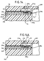
- the heating element sections 211a-211d are formed on the second dielectric layer 296. Portions of the sections 211a-211d extend through the openings 296a in the second dielectric layer 296 positioned above the points 364b and 365b on the final portions 264 and 265 such that the heating element sections 211a-211d directly contact the final portions 264 and 265 of the first conductors 260a-260c, see Fig. 11.
- the lower section of each opening 296a above the points 364b and 365b may be square as shown in Fig. 11A. Alternatively, it may be circular, as shown in Fig. 11B, annular, as shown in Fig. 11C, or may have any other geometric shape.
- the heating element sections 211a-211d may be formed in essentially the same manner as the heating elements sections 11a-11d in the Fig. 3 embodiment and from any one of the materials set out above from which the heating element sections 11a-11d are formed.
- the heating element sections 211a-211d may be rectangular, as shown in Fig. 9.
- the sections 211a-211d may be T-shaped or have another shape not explicitly set out herein.
- smaller heating element sections may be provided, each of which defines only a single heating element.
- the heating elements 212 comprise the heated zones of the heating element sections 211a-211d when current passes through the sections 211a-211d.
- the shape and size of the heated zones is defined generally by the size of the openings 296a.
- the heating elements 212 i.e., the resistive material layer portions extending into the openings 296a and between intersecting sections of the final portions 264 and 265 of the first conductors 260a-260c and the second segments 274 of the second conductors 270a-270d preferably have a substantially constant cross-sectional area along a first axis A 1 which is generally parallel to the direction of current flow between the portions 264 and 265 and the second segments 274, see Fig. 14. Because the cross-sectional area of each heating element 212 in the direction of current flow does not vary, it is believed that generally uniform heating of each heating element 212 will occur.
- each heating element 212 may have a substantially non-uniform cross-sectional area along a second axis A 2 which is generally orthogonal to the first axis A 1 .
- the heated zones, i.e., the heating elements 212, of the heating element sections 211a-211d may be cylindrical in shape such that they have a circular ink-facing surface.
- the heated zones may also comprise hollow cylinders such that they have an annular ink-facing surface. The shape of the heated zones is determined by the shape of the openings 296a.
- the heated zones will be cylindrical in shape. If the openings 296a are annular, the heated zones will have the shape of a hollow cylinder.
- the ink-facing surface of the heated zones or heating elements 212 may have a rounded or curvilinear section, e.g., they may be circular or annular in shape. They may also be square or rectangular in shape and have rounded corners. Consequently, each heating element 212 may be more readily configured so as to minimize damage to the heating element 212 due to concentrated shock waves produced during contraction of air bubbles in the ink. This added benefit may occur without sacrificing heating element efficiency as the cross-sectional area of each heating element 212 remains substantially constant in the direction of current flow.
- each of the two second conductors 270a and 270d Substantially the entire portion of each of the two second conductors 270a and 270d, the beginning portion 262 of the first conductor 260a, upper sections 361b and 361c of the first conductors 260b and 260c, upper sections 371b and 371c of the second conductors 270b and 270c, and the intermediate portions 263 are formed on the dielectric layer 296.
- the second segments 274 of the second conductors 270a-270d extend over the heating element sections 211a-211d, see Figs. 9-11, 13 and 14.
- the portions 262 and 263 and the sections 361b and 361c may be formed in essentially the same manner as the primary conductors 68 of the Fig.
- the conductors 270a and 270d and the sections 371b and 371c may be formed in essentially the same manner as the second conductors 70a-70d of the Fig. 3 embodiment and from any one of the materials set out above from which the conductors 70a-70d are formed.
- the upper section 361b of the first conductor 260b extends through the opening 296a in the dielectric layer 296 above one of the points 361 on the lower section 261b so as to contact the lower section 261b.
- the upper section 361c of the first conductor 260c extends through the opening 296a in the dielectric layer 296 above one of the points 361 on the lower section 261c so as to contact the lower section 261c.
- the two upper sections 371b of the second conductor 270b extend through the openings 296a in the dielectric layer 296 above the points 371 on the lower section 271b so as to contact the lower section 271b.
- the two upper sections 371c of the second conductor 270c extend through the openings 296a in the dielectric layer 296 above the points 371 on the lower section 271c so as to contact the lower section 271c.
- the first and second legs 263a and 263b of each intermediate portion 263 extend through openings 296a in the dielectric layer 296 over points 364a and 365a on corresponding final portions 264 and 265 so as to engage those final portions 264 and 265.
- a central section 263c of the intermediate portion 263 forming part of the first conductor 260b extends through an opening 296a in the dielectric layer 296 so as to engage the lower section 261b.
- a central section 263d of the intermediate portion 263 forming part of the first conductor 260c extends through an opening 296a in the dielectric layer 296 so as to engage the lower section 261c.
- a protective layer 297 is added over the exposed portions of the dielectric layer 296 and the first and second conductors 260a-260c and 270a-270d.
- this layer 297 is formed from, for example, Si 3 N 4 or SiC via art recognized deposition processes.
- the layer 297 may have a thickness of from about 500 angstroms to about 10,000 angstroms.
- the orifice plate 30 is secured to the layer 297 via an adhesive 40.
- a heater chip 310 formed in accordance with a fourth embodiment of the present invention is illustrated in Fig. 14A, wherein like reference numerals indicate like elements.
- the heating element section 311 is formed directly over the final portion 264 of the first conductor 260.
- the second dielectric layer 296 extends over parts of the heating element section 311.
- the second segment 274 of the second conductor 270 is formed over the dielectric layer 296 and extends through three openings 296a in the layer 296 so as to contact the heating element section 311 at three spaced-apart portions along the heating element section 311.
- Each spaced-apart portion of the heating element section 311 comprises a heating element 312.
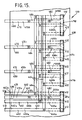
- a heater chip 410 formed in accordance with a fifth embodiment of the present invention, is illustrated in Fig. 15.
- the chip 410 comprises a main body portion 418 including a plurality of first and second conductors 460 and 470.
- the main body portion 418 is constructed in essentially the same manner as the main body portion 218 in the embodiment illustrated in Fig. 9.
- heating element sections 411a-411d are provided on the chip 410 (shown in dotted line in Fig. 9). Portions of the heating element sections 411a-411d define resistive heating elements 412. For ease in understanding, the heating elements 412 are designated by dotted line squares in Fig. 15.
- the embodiment illustrated in Fig. 15 includes three first conductors 460a-460c and four second conductors 470a-470d.
- Each of the first conductors 460a-460c comprises first and second upper portions 462 and 464 and four lower third portions 466a-466d.
- a first end 462a of the first portion 462 is coupled to a bond pad 416.
- the second portion 464 extends generally at a right angle to the first portion 462 and is integral with the first portion 462.
- Each of the four third portions 466a-466d to which a second portion 464 is connected extends below and is positioned in-line with a different one of the four second conductors 470a-470d.
- each of the four second conductors 470a-470d is positioned above and is located in-line with a single third portion of each of the first conductors 460a-460c.
- a second dielectric layer formed in the same manner and from the same material as the dielectric layer 296 in the Fig. 9 embodiment, is positioned between the first and second portions 462 and 464 and the third portions 466a-466d.
- the heating element sections 411a-411d are formed on the second dielectric layer. Openings (not shown), similar to the openings 296a in dielectric layer 296, are formed in the second dielectric layer.
- Each second portion 464 extends through four openings in the second dielectric layer so as to contact its corresponding four third portions 466a-466d.
- the heating element sections 411a-411d extend through openings in the second dielectric layer so as to contact the third portions 466a-466d.
- the heating element sections 411a-411d are rectangular in the illustrated embodiment but may be of any shape. However, the sections 411a-411d should not extend along the upper surface of the second dielectric layer so as to be positioned at locations where the second portions 464 extend through openings in the second dielectric layer to contact the third portions 466a-466d.
- Each of the second conductors 470a-470d comprises first and second upper portions 480 and 482 and a third lower portion 484.
- the second dielectric layer extends over parts of the lower portions 484.
- the first and second portions 480 and 482 are formed on the second dielectric layer and extend through openings in the second dielectric layer so as to contact opposite ends of the lower portions 484.
- the second portions 482 also contact the heating element sections 411a-411d.
- the upper portions 462, 464, 480 and 482 of the first and second conductors 460a-460c and 470a-470d may be formed on the first dielectric layer (not shown) of the main body portion 418 such that they are positioned below the second dielectric layer and the lower portions 466a-466d and 484 may be formed on the upper surface of the second dielectric layer.
- the upper and lower portions and sections of the first and second conductors 260a-260c and 270a-270d in the Fig. 9 embodiment may be reversed such that the upper portions and sections are positioned below the second dielectric layer 296 and the lower portions and sections are positioned on the dielectric layer 296.
Abstract
Description
- This invention relates to ink jet printheads and heater chips having heating elements and conductors for delivering energy to the heating elements.
- Drop-on-demand ink jet printers use thermal energy to produce a vapor bubble in an ink-filled chamber to expel a droplet. A thermal energy generator or heating element, usually a resistor, is located in the chamber on a heater chip near a discharge orifice. A plurality of chambers, each provided with a single heating element, are provided in the printer's printhead. The printhead typically comprises the heater chip and a plate having a plurality of the discharge orifices formed therein. The printhead forms part of an ink jet print cartridge which further comprises an ink-filled container.
- The resistors are individually addressed with an energy pulse to momentarily vaporize the ink and form a bubble which expels an ink droplet. A flexible circuit may be used to provide a path for energy pulses to travel from a printer energy supply circuit to the printhead. Bond pads on the printhead are coupled to end sections of traces on the circuit. A plurality of first and second conductors are provided on the heater chip and extend between the bond pads and the resistors. Current is delivered to the resistors via the traces, the bond pads and the first and second conductors.
- In first generation printheads, the number of first conductors and associated bond pads equaled the number of resistors provided on the chip. However, fewer second conductors, each coupled to two or more resistors, were provided. The first and second conductors were located in generally the same plane as the resistors.
- In order to reduce the number of first conductors and associated bond pads, later printers and printheads were provided with decoder circuitry. Decoder circuitry, however, is expensive and, hence, undesirable.
- Accordingly, there is a need for improved structure within an ink jet printhead for providing energy pulses to heating elements.
- This need is met by the present invention wherein an ink jet printhead is provided having a heater chip including a plurality of first and second conductors arranged in spaced-apart planes and/or in a matrix. When conductors are arranged in a matrix, fewer first and second conductors are required on the heater chip. Additionally, decoder circuitry is substantially reduced or completely eliminated. When the first and second conductors are vertically spaced apart, fewer conductors are located in substantially the same plane as the heating elements. Hence, a higher density of heating elements may be provided on the heater chip.
- In one embodiment, the heating elements are located on a thermally non-conductive layer. For this reason, it is believed that the heater chip of this embodiment has improved thermal efficiency and, hence, requires less energy to effect bubble formation than conventional heater chips.
- Embodiments of the invention will now be described by way of example only and with reference to the accompanying drawings, in which:
- Fig. 1 is a plan view of first and second conductors of a heater chip formed in accordance with a first embodiment of the present invention wherein the first conductors are shown in solid line and the second conductors are shown in dot-dash line;
- Fig. 2 is a plan view of a portion of a heater chip coupled to an orifice plate with sections of the orifice plate removed at two different levels;
- Fig. 3 is a view taken along section line 3-3 in Fig. 2;
- Fig. 4 is a plan view of a portion of a heater chip formed in accordance with a second embodiment of the present invention;
- Fig. 5 is a view taken along view line 5-5 in Fig. 4;
- Fig. 6 is a view taken along view line 6-6 in Fig. 4;
- Fig. 7 is a view taken along view line 7-7 in Fig. 4;
- Fig. 8 is an exploded, cross-sectional view taken through a chip formed in accordance with the second embodiment of the present invention;
- Fig. 9 is a plan view of first and second conductors and heating element sections of a heater chip formed in accordance with a third embodiment of the present invention wherein upper sections of the first and second conductors are shown in solid line and lower sections of the first and second conductors are shown in dotted line;
- Fig. 10 is a view taken along view line 10-10 in Fig. 9;
- Fig. 11 is a view taken along view line 11-11 in Fig. 9;
- Figs. 11A-11C are views of modified openings in the second dielectric layer of the heater chip shown in Fig. 11;
- Fig. 12 is a view taken along view line 12-12 in Fig. 9;
- Fig. 13 is a view taken along view line 13-13 in Fig. 9;
- Fig. 14 is a cross-sectional view taken through a portion of a printhead having a heater chip constructed in accordance with the third embodiment of the present invention;
- Fig. 14A is a cross-sectional view taken through a portion of a printhead having a heater chip constructed in accordance with a fourth embodiment of the present invention; and
- Fig. 15 is a plan view of first and second conductors of a heater chip constructed in accordance with a fifth embodiment of the present invention.
-
- A
heater chip 10, formed in accordance with a first embodiment of the present invention, is illustrated in Figs. 1-3. Anorifice plate 30 is adapted to be secured to thechip 10 via an adhesive 40, see Fig. 3. The coupledchip 10 andplate 30 define an ink jet printhead which is secured to an ink-filled often polymeric container (not shown). The joined polymeric container and printhead form a portion of an ink jet print cartridge which is adapted to be installed in an ink jet printer (not shown). The polymeric container may be capable of being refilled with ink. - In the illustrated embodiment, the
heater chip 10 is provided with a plurality of T-shaped resistiveheating element sections 11a-11d. As will be discussed more explicitly below, portions of theheating element sections 11a-11d defineresistive heating elements 12. While theheating elements 12 in the embodiment illustrated in Figs. 1-3 comprise portions of theheating element sections 11a-11d, theheating elements 12 are designated in Figs. 1 and 2 by squares shown in dotted line to allow for ease in understanding the present invention. - The
plate 30 includesopenings 32 which extend completely through theplate 30 and defineorifices 32a through which ink droplets are ejected.Sections 34 of theplate 30 andportions 14 of theheater chip 10 define a plurality ofbubble chambers 50. The resistiveheating element sections 11a-11d are located on thechip 10 such that a portion of aheating element section 11a-11d, i.e., asingle heating element 12, is associated with each of thebubble chambers 50, see Fig. 3. Ink supplied by the polymeric container flows into acentral opening 15 formed in thechip 10. The ink then moves throughink supply channels 52 into thebubble chambers 50. - The
resistive heating elements 12 are individually addressed by energy pulses. Each energy pulse is applied to aheating element 12 to momentarily vaporize the ink in thebubble chamber 50 with which theheating element 12 is associated to form a bubble within thechamber 50. The function of the bubble is to displace ink within thechamber 50 such that a droplet of ink is expelled through thebubble chamber orifice 32a. - A flexible circuit (not shown) secured to the polymeric container is used to provide a path for energy pulses to travel from a printer energy supply circuit to the
heater chip 10.Bond pads 16, see Fig. 1, on theheater chip 10 are bonded to end sections of traces (not shown) on the flexible circuit. Current flows from the printer energy supply circuit to the traces on the flexible circuit and from the traces to thebond pads 16 on theheater chip 10. - The
heater chip 10 comprises amain body portion 18 including a plurality of first and second conductors. In Fig. 1, first andsecond sets 80a and 80b of sixfirst conductors 60a-60f, four second conductors 70a-70d, and fourheating element sections 11a-11d are shown on opposite sides of thecentral opening 15. Eachheating element section 11a-11d defines sixheating elements 12 such that fourheating element sections 11a-11d provide 24heating elements 12. Thus, the eightheating element sections 11a-11d provide 48heating elements 12. The first andsecond conductors 60a-60f and 70a-70d in each of the first andsecond sets 80a and 80b are arranged in a matrix having first conductor rows and second conductor columns. Each second conductor column is defined by a single second conductor 70a-70d such that four columns are provided which are positioned in-line with one another. Hence, only sixfirst conductors 60a-60f and four second conductors 70a-70d are required to effect the firing of 24heating elements 12. It is contemplated by the present invention that the number ofheating elements 12 and the number of first and second conductors 60 and 70 provided on thechip 10 may be varied. - In the illustrated embodiment, each of the
first conductors 60a-60f comprises oneprimary conductor 62 and foursecondary conductors 68. Theprimary conductor 62 has first andsecond segments first end 64a of thefirst segment 64 is coupled to abond pad 16. Thesecond end 64b of thefirst segment 64 is coupled to asecond segment 66. Thesecond segment 66 is coupled to foursecondary conductors 68 at spaced-apartpoints 66b along its length. Each of the foursecondary conductors 68 to which a givensecond segment 66 is coupled extends below and is positioned in-line with a different one of the four second conductors 70a-70d, see Figs. 1-3. Thus, each of the four second conductors 70a-70d is positioned above and is located in-line with a singlesecondary conductor 68 of each of thefirst conductors 60a-60f. - Each of the second conductors 70a-70d comprises a
first segment 72 and asecond segment 74 which is substantially transverse to thefirst segment 72. A first end 72a of thefirst segment 72 is coupled to abond pad 16 while asecond end 72b of thefirst segment 72 is coupled to thesecond segment 74 at an intermediate point along thesecond segment 74. Eachsecond segment 74 extends over and contacts sixheating elements 12. - In order to effect the firing of a given
heating element 12, current is passed through thefirst conductor 60a-60f which is positioned directly below theheating element 12 and the second conductor 70a-70d which is positioned above and contacts theheating element 12. For example, heating element 12a in Fig. 1 is fired by passing current through thefirst conductor 60b and thesecond conductor 70b.Heating element 12b is fired by passing current through thefirst conductor 60a and thesecond conductor 70d. - In the embodiment illustrated in Figs. 1-3, the
main body portion 18 further includes abase portion 90 and afirst dielectric layer 92 formed over thebase portion 90. Thebase portion 90 may be formed from silicon, i.e., it may comprise a silicon wafer section. Alternatively, thebase portion 90 may be formed from any other substrate material which is substantially ink resistant, such as alumina or stainless steel. Thedielectric layer 92 may be formed from any commercially available dielectric material, such as silicon dioxide or silicon nitride. Thebase portion 90 preferably has a thickness of from about 400 µm to about 800 µm, as measured in the Z-direction, see Fig. 3. Thedielectric layer 92 preferably has a thickness of from about 0.1 µm to about 5.0 µm. If thedielectric layer 92 is formed from silicon dioxide, it may be formed via a conventional thermal oxidation, sputtering or chemical vapor deposition process. If thedielectric layer 92 is formed from silicon nitride, it may be formed via a sputtering or chemical vapor deposition process. - The
primary conductors 62, including both the first andsecond segments dielectric layer 92. Aluminum or any other highly conductive material, such as copper or gold, may be employed. For example, a layer of aluminum may be added to thedielectric layer 92 via a conventional vacuum evaporation process. Alternatively, a conventional sputter deposition process may be employed. A conventional photomasking process is then used to remove unwanted metal such that the remaining metal defines theprimary conductors 62. It is also contemplated that a conventional lift-off photolithography process may be used to remove the unwanted metal. The lift-off process involves forming a photoresist layer (also referred to herein as a resist layer) on thedielectric layer 92 before adding the aluminum material. During a development step, resist material located in areas where theconductors 62 are to be formed is removed. The aluminum layer is then deposited. Thereafter, remaining resist material and aluminum formed over the remaining resist material are removed. The aluminum not removed defines theprimary conductors 62. Theconductors 62 preferably have a thickness of from about 0.2 µm to about 2 µm, as measured in the Z-direction, see Fig. 3. Thefirst segments 64 preferably have a width of from about 10 µm to about 100 µm, as measured in the Y-direction, and thesecond segments 66 preferably have a width of from about 10 µm to about 100 µm, as measured in the X-direction. - A second dielectric layer 96 is formed over the exposed portions of the
dielectric layer 92 and theconductors 62. The layer 96 is preferably formed from any one of a number of commercially available polymeric photoresist materials. An example of such a material is a negative acting photoresist material, which is commercially available from Shipley Company Inc. under the product name "MEGAPOSIT SNR™ 248 PHOTO RESIST." The dielectric layer 96 extends into areas between theconductors 62 so as to prevent current movement betweenadjacent conductors 62. The layer 96 also covers theconductors 62 except at thepoints 66b where thesecond segments 66 of theconductors 62 are to be coupled to thesecondary conductors 68, see Fig. 3. A conventional material removal process, a development process in the illustrated embodiment, is used to remove portions of the dielectric layer 96 located above thepoints 66b so as to formopenings 96a in the layer 96. The dielectric layer 96, at locations not covering theconductors 62, preferably has a thickness of from about 1 µm to about 5 µm, as measured in the Z-direction, see Fig. 3. - The
secondary conductors 68 are added to the dielectric layer 96 such that they are positioned in a first horizontal plane P1, see Fig. 3. Theconductors 68 are preferably formed from aluminum or a like material via a conventional vacuum evaporation process and a photomasking process. Alternatively, theconductors 68 may be formed via a conventional sputter deposition process and/or a lift-off photolithography process. The aluminum material extends through theopenings 96a in the dielectric layer 96. Hence, thesecondary conductors 68 extend through theopenings 96a in the layer 96 and engage thesecond segments 66 of theconductors 62 atpoints 66b. Theconductors 68 preferably have a thickness of from about 0.2 µm to about 2 µm, as measured in the Z-direction, and a width of from about 10 µm to about 100 µm, as measured in the Y-direction, see Fig. 3. - A
third dielectric layer 98 is added over the exposed portions of the dielectric layer 96 and theconductors 68. Thelayer 98 preferably comprises the same material from which the dielectric layer 96 is formed. Thelayer 98 extends into areas between theconductors 68 so as to prevent current movement betweenadjacent conductors 68. Thelayer 98 also extends over theconductors 68. However, a conventional material removal process, a development process in the illustrated embodiment, is used to form openings 98a in thedielectric layer 98 located aboveend regions 68a of theconductors 68, whichregions 68a are positioned in-line with theheating elements 12, see Fig. 3. The openings 98a may be square in shape having a length along each side which is from about 15 microns to about 50 microns and preferably about 30 microns. The openings 98a may also be circular, elliptical, annular or rectangular in shape. If the openings 98a are square or rectangular, they may have rounded corners. Thedielectric layer 98, at regions not positioned over aconductor 68, preferably has a thickness of from about 1 µm to about 5 µm, as measured in the Z-direction, see Fig. 3. - In the Fig. 3 embodiment, a
current transfer layer 100 is added to thedielectric layer 98. It extends through the openings 98a in thedielectric layer 98 so as to engage theend regions 68a of theconductors 68. Preferably, the material from which thelayer 100 is formed is electrically conductive so as to allow current to flow between thefirst conductors 60a-60f and theheating elements 12. The material, however, should not be so conductive as to allow current to flow substantially into a neighboringheating element 12. The resistivity of the material is preferably from about 0.1 W-cm to about 5 W-cm, and more preferably about 1 W-cm. It is also preferred that the material be temperature resistant if heated to a temperature of less than about 350°C for about 5 mseconds. It is further preferred that the material be thermally non-conductive. The thermal conductivity of the material is preferably from about 0.1 W/m°C to about 15 W/m°C, and more preferably from about 0.1 W/m°C to about 0.5 W/m°C. Most preferably, the material is a high temperature resistant polymer loaded with an electrically conductive filler. An example of such a material is a carbon-filled polyimide material. Such a material may be formed by blending a commercially available polyimide material with a carbon black material such that the latter is generally evenly dispersed throughout the polyimide material. Thecurrent transfer layer 100 may be formed via a conventional spin application process followed by a conventional oven curing process. Thelayer 100 preferably has a thickness of from about 5 µm to about 50 µm, as measured in the Z-direction, see Fig. 3. - The
heating element sections 11a-11d are formed on thecurrent transfer layer 100, see Fig. 3. The resistive material from which theheating element sections 11a-11d are formed preferably comprises TaOx. X is < 2 and preferably << 1, thus indicating a substantially non-stoichiometric condition. This material may be deposited via a reactive sputtering process. During that process, oxygen gas along with an inert working gas is added to a vacuum chamber. The oxygen gas reacts with the tantalum vapor material in the chamber so as to deposit as TaOx. The pressure of the oxygen gas in the chamber is varied so as to vary the stoichiometry of the material. Other materials such as aluminum oxide may be used to form theheating element sections 11a-11d. Preferably, theheating element sections 11a-11d have a resistivity which is from about 10 W-cm to about 400 W-cm, and preferably is about 40 W-cm for a thickness of about 1000 angstroms, when measured in the Z-direction, see Fig. 3. The thickness of theheating element sections 11a-11d is preferably from about 800 angstroms to about 10,000 angstroms. - In the illustrated embodiment, the
heating element sections 11a-11d comprise four discrete T-shapedsections 11a-11d. A photomasking or a lift-off photolithography process may be used to remove unwanted resistive material so as to form the fourheating element sections 11a-11d. In another embodiment, the resistive material removal step is not performed such that a blanket of resistive material remains on thecurrent transfer layer 100. In this and the Fig. 1 embodiments, theheating elements 12 comprise resistive material layer portions which are located between intersecting sections of the first andsecond conductors 60a-60f and 70a-70d. More specifically, theheating elements 12 comprise the heated zones of theheating element sections 11a-11d when current passes through thesections 11a-11d. The size of the heated zones is defined generally by the size of the openings 98a. Thus, for square openings 98a having 30 micron sides, the surface area of each of theheating elements 12 is about 9 x 10⁻¹⁰ m2. As noted above, the resistive material layer portions which comprise theheating elements 12 are designated by squares shown in dotted line in Figs. 1 and 2. - The
heating elements 12, i.e., the resistive material layer portions between intersecting sections of the first andsecond conductors 60a-60f and 70a-70d, preferably have a substantially constant cross-sectional area along a first axis A1 which is generally parallel to the direction of current flow between the first andsecond conductors 60a-60f and 70a-70d, see Fig. 3. Because the cross-sectional area of eachheating element 12 in the direction of current flow does not vary, it is believed that generally uniform heating of eachheating element 12 will occur. This is in contrast to a heating element having a non-uniform cross-section area in the direction of current flow. In such a heating element, it is believed that "hot" and "cold" zones may result when current passes through it. "Cold" zones reduce the overall efficiency of the heating element and may adversely affect print quality. - Because current flow in the present invention occurs along a generally vertical axis which passes through the heating element upper surface, i.e., the surface closest to the ink-containing
chamber 50, eachheating element 12 may have a substantially non-uniform cross-sectional area along a second axis A2 which is generally orthogonal to the first axis A1. Thus, the heated zones, i.e., theheating elements 12, of theheating element sections 11a-11d may be cylindrical in shape such that they have a circular ink-facing surface. The heated zones may also comprise hollow cylinders such that they have an annular ink-facing surface. The shape of the heated zones is determined by the shape of the openings 98a. If the openings 98a are circular, the heated zones will be cylindrical in shape. If the openings 98a are annular, the heated zones will have the shape of a hollow cylinder. Thus, the ink-facing surface of the heated zones orheating elements 12 may have a rounded or curvilinear section, e.g., they may be circular or annular in shape. They may also be square or rectangular in shape and have rounded corners. Consequently, the heating elements may be more readily configured so as to minimize damage to the heating elements due to concentrated shock waves produced during contraction of air bubbles in the ink. This added benefit may occur without sacrificing heating element efficiency as the cross-sectional area of eachheating element 12 remains substantially constant in the direction of current flow. - The second conductors 70a-70d are formed over the
heating element sections 11a-11d. So as to prevent current from bypassing theheating elements 12 and flowing directly between thecurrent transfer layer 100 and one of the second conductors 70a-70d, the second conductors 70a-70d do not contact thecurrent transfer layer 100 in areas close to the openings 98a in thedielectric layer 98. In the illustrated embodiment, the second conductors 70a-70d are coextensive with theheating element sections 11a-11d and, hence, do not contact thecurrent transfer layer 100. The second conductors 70a-70d are positioned in a second horizontal plane P2 which is vertically spaced from the first horizontal plane P1, see Fig. 3. The second conductors 70a-70d may be created, for example, from tantalum using a conventional sputter deposition process followed by conventional photomasking and etch back processes. Alternatively, a conventional vacuum evaporation process and a lift-off photolithography process may be used. Metals which are substantially non-reactive with ink, such as gold, may be used instead of tantalum. Other metals may also be used such as aluminum, copper and alloys prepared therefrom provided there is a passivation (protective) layer provided over the second conductors 70a-70d. - The tantalum layer may be applied in the same sputtering run during which the
heating element sections 11a-11d are formed. This is accomplished by adding only an inert working gas into the vacuum chamber after the layer of TaOx has been formed. If the lift-off process is employed, a stripping solution is used to remove the photoresist material. The unwanted TaOx and tantalum material are removed with the photoresist material. The remaining TaOx resistive material defines the heating element sections 11-11d, which have substantially the same T-shape as the second conductors 70a-70d. Thus, theheating elements 12 comprise portions of the T-shapedsections 11a-11d positioned between intersecting sections of the first andsecond conductors 60a-60f and 70a-70d. The second conductors 70a-70d preferably have a thickness of from about 0.2 µm to about 2 µm when measured in the Z-direction, and a width of from about 10 µm to about 100 µm as measured in the X-direction. - After the second conductors 70a-70d have been formed, the
orifice plate 30 is secured to thecurrent transfer layer 100 and the second conductors 70a-70d via an adhesive 40. An example of such anorifice plate 30 and example adhesives are set out in commonly owned patent application, U.S. Serial No. 08/519,906, entitled "METHOD OF FORMING AN INKJET PRINTHEAD NOZZLE STRUCTURE," by Tonya H. Jackson et al., filed on August 28, 1995, Attorney Docket No. LE9-95-024, the disclosure of which is hereby incorporated by reference. As noted therein, theplate 30 may be formed from a polymeric material such as polyimide, polyester, fluorocarbon polymer, or polycarbonate, which is preferably about 15 to about 200 microns thick, and most preferably about 75 to about 125 microns thick. The adhesive may comprise any B-stageable thermal cure resin including phenolic resins, resorcinol resins, urea resins, epoxy resins, ethylene-urea resins, furane resins, polyurethanes, and silicone resins. Other suitable adhesive materials include macromolecular thermoplastic, or hot melt, materials such as ethylene-vinyl acetate, ethylene ethylacrylate, polypropylene, polystryrene, polyamides, polyesters and polyurethanes. - As noted above, in order to effect the firing of a given
heating element 12, current is passed through thefirst conductor 60a-60f which is positioned directly below thatheating element 12 and the second conductor 70a-70d which engages theelement 12. Thecurrent transfer layer 100, which is positioned between the first conductor and theheating element 12, provides a path for current to flow in the Z-direction between the first conductor and theheating element 12. If the first conductor is positive, current passes in the Z-direction from the first conductor through thecurrent transfer layer 100 and theheating element 12 to the second conductor. If the second conductor is positive, the current flows in the Z-direction from the second conductor through theheating element 12 and thecurrent transfer layer 100 to the first conductor. - A
heater chip 110 formed in accordance with a second embodiment of the present invention is illustrated in Figs. 4-8, wherein like reference numerals indicate like elements. Thechip 110 comprises amain body portion 118 including a plurality of first andsecond conductors second conductors - In the Fig. 4 embodiment, two T-shaped
heating element sections chip 110. Portions of theheating element sections resistive heating elements 112. For ease in understanding, theheating elements 112 are designated by dotted line squares in Fig. 4. - Four first conductors 160a-160d are illustrated in Fig. 4. Each of the first conductors 160a-160d comprises one
primary conductor 162 and a plurality ofsecondary conductors 168, two in the embodiment illustrated in Fig. 4. Eachprimary conductor 162 has first andsecond segments first end 164a of thefirst segment 164 is coupled to abond pad 116. Thesecond end 164b of thefirst segment 164 is coupled to asecond segment 166. Thesecond segment 166 is coupled to its twosecondary conductors 168 at spaced-apartpoints 166b along its length, see Fig. 5. Each of the twosecondary conductors 168 to which a givensecond segment 166 is coupled extends below and is positioned in-line with a different one of the twosecond conductors 170, see Figs. 4 and 5. Thus, each of the twosecond conductors 170 is positioned above and is located in-line with a singlesecondary conductor 168 of each of the first conductors 160a-160d. - Each of the
second conductors 170 comprises afirst segment 172 and asecond segment 174 which is substantially transverse to thefirst segment 172. A first end 172a of thefirst segment 172 is coupled to abond pad 116 while asecond end 172b of thefirst segment 172 is coupled to thesecond segment 174 at an intermediate point along thesecond segment 174. - In order to effect the firing of a given
heating element 112, current is passed through thefirst conductor 160 which is positioned directly below thatheating element 112 and thesecond conductor 170 which engages theelement 112. - In this embodiment, the chip is not constructed on a silicon wafer or like substrate material. Rather, the chip is formed by initially providing a
substrate 120 comprising integral dielectric and current transfer layers 122 and 124. Thedielectric layer 122, also referred to herein as a first dielectric layer, preferably comprises a polymeric material such as a polyimide material. Thecurrent transfer layer 124 preferably comprises a high temperature resistant polymer loaded with an electrically conductive filler, such as a carbon-filled polyimide material. Thecurrent transfer layer 124 preferably has a resistivity which is from about 0.1 W-cm to about 5 W-cm, and more preferably about 1 W-cm. The thermal conductivity of thecurrent transfer layer 124 is preferably from about 0.1 W/m°C to about 3.0 W/m°C, and more preferably about 0.37 W/m°C. Thedielectric layer 122 preferably has a thickness of from about 1 µm to about 100 µm, more preferably from about 1 µm to about 20 µm and most preferably from about 1 µm to about 5 µm. Thecurrent transfer layer 124 preferably has a thickness of from about 1 µm about 100 µm, more preferably from about 1 µm to about 20 µm and most preferably from about 1 µm to about 5 µm. An example of such a substrate is one which is commercially available from DuPont Films under the product designation "KAPTON® XC." - Portions of the
dielectric layer 122 positioned directly below locations where theheating elements 112 are to be positioned on thecurrent transfer layer 124 are removed via a conventional laser ablation process, see opening 122a in Fig. 7. Laser ablation is accomplished at an energy density level of about 100 millijoules/centimeter2 to about 5,000 millijoules/centimeter2, and preferably about 1,000 millijoules/centimeter2. During the laser ablation process, a laser beam with a wavelength of from about 150 nanometers to about 400 nanometers, and most preferably about 248 nanometers, is applied in pulses lasting from about one nanosecond to about 200 nanoseconds, and most preferably about 20 nanoseconds. Theopenings 122a are not limited to any particular shape and may be square, rectangular, circular or annular in shape. - The
secondary conductors 168 are added to thefirst dielectric layer 122 and extend along a first horizontal plane P1, see Fig. 7. Theconductors 168 are preferably formed from aluminum or a like material via conventional vacuum evaporation and photomasking processes. Alternatively, a sputter deposition process and/or a lift-off photolithography process may be used. The aluminum material extends through theopenings 122a in thedielectric layer 122, see Fig. 7. Hence, thesecondary conductors 168 engage thecurrent transfer layer 124. Theconductors 168 preferably have a thickness of from about 0.2 µm to about 2 µm, as measured in the Z-direction, and a width of from about 40 µm to about 400 µm, as measured in the Y-direction, see Fig. 7. - A
second dielectric layer 195 is added over the exposed portions of thedielectric layer 122 and theconductors 168. Thelayer 195 preferably comprises the same material from which the dielectric layer 96, discussed above, is formed. Thelayer 195 extends into areas between theconductors 168 so as to prevent current movement betweenadjacent conductors 168. Thelayer 195 also extends over theconductors 168. However, a conventional material removal process, a development process in the illustrated embodiment, is used to remove portions of thedielectric layer 195 positioned directly above locations where thesecond segments 166 are to be coupled to theconductors 168, i.e., overpoints 166b on thesecond segments 166. Thedielectric layer 195, at regions not positioned over aconductor 168, preferably has a thickness of from about 1 µm to about 5 µm, as measured in the Z-direction, see Fig. 7. - The
primary conductors 162, including the first andsecond segments dielectric layer 195. Aluminum or any other highly conductive material, such as copper or gold, may be employed. For example, a layer of aluminum may be added to thedielectric layer 195 via a conventional vacuum evaporation process. Alternatively, a conventional sputter deposition process or other similar process may be employed. A conventional photomasking process is then used to remove unwanted metal such that the remaining metal defines theprimary conductors 162. It is also contemplated that a conventional lift-off photolithography process may be used to remove the unwanted metal. Theconductors 162 preferably have a thickness of from about 0.2 µm to about 2 µm, and a width of from about 10 µm to about 100 µm. - A
protective layer 197 is added over the exposed portions of thedielectric layer 122 and theconductors 168. Preferably, thislayer 197 is formed from solder mask via a conventional spray or roll lamination process. Thelayer 197 preferably has a thickness, as measured in the Z-direction, of from about 10 µm to about 100 µm. - The
heating element sections current transfer layer 124. Preferably, theheating element sections heating element sections 11a-11d of the embodiment illustrated in Figs. 1-3. Thesecond conductors 170 are formed over theheating element sections second conductors 170 are preferably formed from substantially the same materials and in substantially the same way as the second conductors 70a-70d of the embodiment illustrated in Figs. 1-3. - After the
second conductors 170 have been formed, theorifice plate 30 is secured to thecurrent transfer layer 124 and thesecond conductors 170 via an adhesive 40, see Fig. 8. - Because the
current transfer layer current transfer layer - It is believed that heater chips constructed in accordance with the first and second embodiments of the present invention having
heating elements 12 with a resistance of from about 300 W to about 600 W require a current pulse having an amplitude of from about 5 to about 30 milliamps and a pulse width of from about 1 µs to 5 µs and preferably about 2 µs to cause a droplet of ink to be expelled through a bubble chamber orifice. - In a test device having a single heating element, bubble formation was achieved when the heating element, which had a resistance of about 400 W, received a current pulse having a pulse width of about 2 µs and an amplitude of from about 7.5 mA to about 20 mA. Voltage was from about 3V to about 8V and power/pulse was less than about 0.32 µj/pulse. The heating element or heated zone was substantially circular in shape and had a diameter of about 20 µm to about 30 µm. The thickness of the heating element was about 1000 µm. In contrast, about 6-7 µj/pulse is required to effect bubble formation with a conventional heater chip. Thus, this test device provided approximately a 10 times reduction in the amount of power needed to achieve bubble formation.
- The following example is being provided for illustrative purposes only and is not intended to be limiting.
- A computer simulation of a printhead including a heater chip in accordance with the second embodiment of the present invention was used. The simulated chip included an aluminum oxide heating element continuous layer having a thickness in the Z-direction of about 0.1 mm, a resistivity of about 2 W-m, a density of about 3800 Kg/m3, a thermal conductivity of 30 W/m°C, and a specific heat of about 1580 J/Kg°C. The
current transfer layer 124 had a thickness in the Z-direction of about 20 mm, a resistivity of about 0.006 W-m, a density of about 1200 Kg/m3, a thermal conductivity of 0.37 W/m°C, and a specific heat of about 1305 J/Kg °C. The width of the positive andnegative conductors - It is further contemplated that a chip formed in accordance with the present invention may include a plurality of heating element sections, each of which defines only a single heating element. Each heating element section is preferably sized larger than its
corresponding opening 98a or 122a in thedielectric layer openings 98a and 122a. Theopenings 98a and 122a may be circular, annular, square, or rectangular in shape. They may also have other geometric shapes not explicitly set out herein. - In order to prevent current from bypassing the heating elements and flowing directly between the second conductors and the current transfer layer, a dielectric layer is formed over the surface of the current transfer layer. Openings having substantially the same shape and size as the
openings 98a or 122a are formed in the dielectric layer. When the heating element sections are formed on the dielectric layer, they extend through the openings in the dielectric layer and directly contact the current transfer layer. When the second conductors are subsequently formed, they do not contact the current transfer layer due to the presence of the dielectric layer surrounding the heating element sections. The dielectric layer formed over the current transfer layer may be formed from the same material used to form layer 96 in the Fig. 3 embodiment. - A
heater chip 210, formed in accordance with a third embodiment of the present invention, is illustrated in Figs. 9-14. Thechip 210 comprises amain body portion 218 including a plurality of first andsecond conductors - Four generally rectangular
heating element sections 211a-211d are provided on the chip 210 (shown in dotted line in Fig. 9). Portions of theheating element sections 211a-211d defineresistive heating elements 212. For ease in understanding, theheating elements 212 are designated by dotted line squares in Fig. 9. - The embodiment illustrated in Fig. 9 includes three
first conductors 260a-260c and foursecond conductors 270a-270d. Each of thefirst conductors 260a-260c comprises a generallylinear beginning portion 262, a generally U-shapedintermediate portion 263, a first generally U-shapedfinal portion 264 and a second generally U-shapedfinal portion 265. A first end 262a of the beginningportion 262 is coupled to abond pad 216. A second, opposingend 262b of the beginning portion is 262 is integral with or in contact with a correspondingintermediate portion 263. Theintermediate portion 263 has first andsecond legs first leg 263a is in contact with a corresponding firstfinal portion 264 and thesecond leg 263b is in contact with a corresponding secondfinal portion 265. The firstfinal portion 264 has first andsecond legs final portion 265 has third andfourth legs 265a and 265b. Thefirst leg 264a extends below and is positioned in-line with thesecond conductor 270a, thesecond leg 264b extends below and is positioned in-line with thesecond conductor 270b, the third leg 264c extends below and is positioned in-line with thesecond conductor 270c, and the fourth leg 264c extends below and is positioned in-line with the second conductor 270d. Thus, each of the foursecond conductors 270a-270d is positioned above and located in-line with a leg of each of the threefirst conductors 260a-260c. - Each of the
second conductors 270 comprises afirst segment 272 and asecond segment 274 which is substantially transverse to thefirst segment 272. Afirst end 272a of thefirst segment 272 is coupled to abond pad 216 while asecond end 272b of thefirst segment 272 is coupled to a correspondingsecond segment 274 at an intermediate point along thesecond segment 274. - In order to effect the firing of a given
heating element 212, current is passed through thefirst conductor 260 which is positioned directly below and engages theheating element 212 and thesecond conductor 270 which extends over and engages theheating element 212. - In this embodiment, the
main body portion 218 further includes abase portion 290 and a firstdielectric layer 292 formed over thebase portion 290, see Figs. 10-14. Thebase portion 290 may be formed from any one of the materials set out above from which thebase portion 90 in the Fig. 3 embodiment is formed. Thefirst layer 292 may be formed in essentially the same manner as thedielectric layer 92 in the Fig. 3 embodiment and from any one of the materials set out above from which thelayer 92 is formed. - The first and second
final portions first conductors 260a-260c,lower sections 261b and 261c of thefirst conductors lower sections second conductors dielectric layer 292. Thefinal portions lower sections primary conductors 62 in the Fig. 3 embodiment and from any one of the materials set out above from which theconductors 62 are formed. - A
second dielectric layer 296 is formed over the exposed parts of thedielectric layer 292, thefinal portions lower sections dielectric layer 296 may be formed in essentially the same manner as the layer 96 in the Fig. 3 embodiment and from the same material from which the layer 96 is formed. - The
dielectric layer 296 extends into areas between thefinal portions lower sections layer 296 also covers thefinal portions lower sections points final portions lower sections dielectric layer 296 located above thepoints openings 296a in the layer 96, see Figs. 11-13. - The
heating element sections 211a-211d are formed on thesecond dielectric layer 296. Portions of thesections 211a-211d extend through theopenings 296a in thesecond dielectric layer 296 positioned above thepoints final portions heating element sections 211a-211d directly contact thefinal portions first conductors 260a-260c, see Fig. 11. The lower section of eachopening 296a above thepoints heating element sections 211a-211d may be formed in essentially the same manner as theheating elements sections 11a-11d in the Fig. 3 embodiment and from any one of the materials set out above from which theheating element sections 11a-11d are formed. Theheating element sections 211a-211d may be rectangular, as shown in Fig. 9. Alternatively, thesections 211a-211d may be T-shaped or have another shape not explicitly set out herein. Further, smaller heating element sections may be provided, each of which defines only a single heating element. - The
heating elements 212 comprise the heated zones of theheating element sections 211a-211d when current passes through thesections 211a-211d. The shape and size of the heated zones is defined generally by the size of theopenings 296a. - The
heating elements 212, i.e., the resistive material layer portions extending into theopenings 296a and between intersecting sections of thefinal portions first conductors 260a-260c and thesecond segments 274 of thesecond conductors 270a-270d preferably have a substantially constant cross-sectional area along a first axis A1 which is generally parallel to the direction of current flow between theportions second segments 274, see Fig. 14. Because the cross-sectional area of eachheating element 212 in the direction of current flow does not vary, it is believed that generally uniform heating of eachheating element 212 will occur. - Since current flow in the present invention occurs along a generally vertical axis which passes through the heating element upper surface, i.e., the surface closest to the ink-containing chamber, each
heating element 212 may have a substantially non-uniform cross-sectional area along a second axis A2 which is generally orthogonal to the first axis A1. Thus, the heated zones, i.e., theheating elements 212, of theheating element sections 211a-211d may be cylindrical in shape such that they have a circular ink-facing surface. The heated zones may also comprise hollow cylinders such that they have an annular ink-facing surface. The shape of the heated zones is determined by the shape of theopenings 296a. If theopenings 296a are circular, the heated zones will be cylindrical in shape. If theopenings 296a are annular, the heated zones will have the shape of a hollow cylinder. Thus, the ink-facing surface of the heated zones orheating elements 212 may have a rounded or curvilinear section, e.g., they may be circular or annular in shape. They may also be square or rectangular in shape and have rounded corners. Consequently, eachheating element 212 may be more readily configured so as to minimize damage to theheating element 212 due to concentrated shock waves produced during contraction of air bubbles in the ink. This added benefit may occur without sacrificing heating element efficiency as the cross-sectional area of eachheating element 212 remains substantially constant in the direction of current flow. - Substantially the entire portion of each of the two
second conductors 270a and 270d, the beginningportion 262 of thefirst conductor 260a,upper sections 361b and 361c of thefirst conductors upper sections second conductors intermediate portions 263 are formed on thedielectric layer 296. Thesecond segments 274 of thesecond conductors 270a-270d extend over theheating element sections 211a-211d, see Figs. 9-11, 13 and 14. Theportions sections 361b and 361c may be formed in essentially the same manner as theprimary conductors 68 of the Fig. 3 embodiment and from any one of the materials set out above from which theprimary conductors 68 are formed. Theconductors 270a and 270d and thesections - The upper section 361b of the
first conductor 260b extends through theopening 296a in thedielectric layer 296 above one of thepoints 361 on the lower section 261b so as to contact the lower section 261b. Theupper section 361c of thefirst conductor 260c extends through theopening 296a in thedielectric layer 296 above one of thepoints 361 on thelower section 261c so as to contact thelower section 261c. The twoupper sections 371b of thesecond conductor 270b extend through theopenings 296a in thedielectric layer 296 above thepoints 371 on thelower section 271b so as to contact thelower section 271b. The twoupper sections 371c of thesecond conductor 270c extend through theopenings 296a in thedielectric layer 296 above thepoints 371 on thelower section 271c so as to contact thelower section 271c. The first andsecond legs intermediate portion 263 extend throughopenings 296a in thedielectric layer 296 overpoints 364a and 365a on correspondingfinal portions final portions intermediate portion 263 forming part of thefirst conductor 260b extends through anopening 296a in thedielectric layer 296 so as to engage the lower section 261b. A central section 263d of theintermediate portion 263 forming part of thefirst conductor 260c extends through anopening 296a in thedielectric layer 296 so as to engage thelower section 261c. - A
protective layer 297 is added over the exposed portions of thedielectric layer 296 and the first andsecond conductors 260a-260c and 270a-270d. Preferably, thislayer 297 is formed from, for example, Si3N4 or SiC via art recognized deposition processes. Thelayer 297 may have a thickness of from about 500 angstroms to about 10,000 angstroms. - After the
protective layer 297 has been formed, theorifice plate 30 is secured to thelayer 297 via an adhesive 40. - A
heater chip 310 formed in accordance with a fourth embodiment of the present invention is illustrated in Fig. 14A, wherein like reference numerals indicate like elements. In this embodiment, theheating element section 311 is formed directly over thefinal portion 264 of thefirst conductor 260. Thesecond dielectric layer 296 extends over parts of theheating element section 311. Thesecond segment 274 of thesecond conductor 270 is formed over thedielectric layer 296 and extends through threeopenings 296a in thelayer 296 so as to contact theheating element section 311 at three spaced-apart portions along theheating element section 311. Each spaced-apart portion of theheating element section 311 comprises aheating element 312. - A
heater chip 410, formed in accordance with a fifth embodiment of the present invention, is illustrated in Fig. 15. Thechip 410 comprises amain body portion 418 including a plurality of first andsecond conductors main body portion 418 is constructed in essentially the same manner as themain body portion 218 in the embodiment illustrated in Fig. 9. - Four generally rectangular
heating element sections 411a-411d are provided on the chip 410 (shown in dotted line in Fig. 9). Portions of theheating element sections 411a-411d defineresistive heating elements 412. For ease in understanding, theheating elements 412 are designated by dotted line squares in Fig. 15. - The embodiment illustrated in Fig. 15 includes three
first conductors 460a-460c and four second conductors 470a-470d. Each of thefirst conductors 460a-460c comprises first and secondupper portions third portions 466a-466d. Afirst end 462a of thefirst portion 462 is coupled to abond pad 416. Thesecond portion 464 extends generally at a right angle to thefirst portion 462 and is integral with thefirst portion 462. Each of the fourthird portions 466a-466d to which asecond portion 464 is connected extends below and is positioned in-line with a different one of the four second conductors 470a-470d. Thus, each of the four second conductors 470a-470d is positioned above and is located in-line with a single third portion of each of thefirst conductors 460a-460c. - A second dielectric layer, formed in the same manner and from the same material as the
dielectric layer 296 in the Fig. 9 embodiment, is positioned between the first andsecond portions third portions 466a-466d. Theheating element sections 411a-411d are formed on the second dielectric layer. Openings (not shown), similar to theopenings 296a indielectric layer 296, are formed in the second dielectric layer. Eachsecond portion 464 extends through four openings in the second dielectric layer so as to contact its corresponding fourthird portions 466a-466d. Likewise, theheating element sections 411a-411d extend through openings in the second dielectric layer so as to contact thethird portions 466a-466d. Theheating element sections 411a-411d are rectangular in the illustrated embodiment but may be of any shape. However, thesections 411a-411d should not extend along the upper surface of the second dielectric layer so as to be positioned at locations where thesecond portions 464 extend through openings in the second dielectric layer to contact thethird portions 466a-466d. - Each of the second conductors 470a-470d comprises first and second
upper portions lower portion 484. The second dielectric layer extends over parts of thelower portions 484. The first andsecond portions lower portions 484. Thesecond portions 482 also contact theheating element sections 411a-411d. - It is further contemplated that the
upper portions second conductors 460a-460c and 470a-470d may be formed on the first dielectric layer (not shown) of themain body portion 418 such that they are positioned below the second dielectric layer and thelower portions 466a-466d and 484 may be formed on the upper surface of the second dielectric layer. - It is further contemplated that the upper and lower portions and sections of the first and
second conductors 260a-260c and 270a-270d in the Fig. 9 embodiment may be reversed such that the upper portions and sections are positioned below thesecond dielectric layer 296 and the lower portions and sections are positioned on thedielectric layer 296.
Claims (39)
- A heater chip comprising:a main body portion; andat least one heating element provided on said main body portion, said main body portion including at least one first conductor and at least one second conductor for providing energy to said at least one heating element, said first conductor being positioned in a first plane and said second conductor being positioned in a second plane which is spaced from said first plane.
- A heater chip as set forth in claim 1, further comprising a current transfer layer interposed between said first conductor and said heating element.
- A heater chip as set forth in claim 1, wherein an insulating layer is not positioned between said first conductor and said heating element.
- A heater chip as set forth in claim 3, wherein said first conductor is vertically spaced from said heating element such that it does not contact said heating element.
- A heater chip as set forth in any preceding claim, wherein said first conductor comprises a primary conductor and a secondary conductor.
- A heater chip as set forth in claim 5, wherein said main body portion further comprises:a base portion;a first dielectric layer positioned over said base portion, said primary conductor being formed on said first dielectric layer;a second dielectric layer provided over portions of said first dielectric layer and portions of said primary conductor, said secondary conductor being formed on said second dielectric layer;a third dielectric layer provided over portions of said second dielectric layer and portions of said secondary conductor; anda current transfer layer extending over portions of said third dielectric layer and end regions of said secondary conductor, said at least one heating element being positioned on said current transfer layer and said second conductor extending to said heating element such that current flows to said heating element through said first and second conductors.
- A heater chip as set forth in claim 5, wherein said main body portion further comprises:a first dielectric layer having said secondary conductor formed on a first side thereof and including an opening through which said secondary conductor extends;a second dielectric layer extending over portions of said first dielectric layer and portions of said secondary conductor, said primary conductor being formed on said second dielectric layer; anda current transfer layer located on a second side of said first dielectric layer and engaging said secondary conductor, said at least one heating element being positioned on said current transfer layer and said second conductor contacting said heating element such that current flows to said heating element through said first and second conductors.
- A heater chip as set forth in claim 7, wherein said first dielectric layer and said current transfer layer comprise an integral film substrate.
- A heater chip as set forth in any of claims 5 to 8, wherein said primary conductor has a first end which is coupled to a bond pad and a second end which is coupled to a first end of said secondary conductor, said secondary conductor having an end which is vertically aligned with said heating element.
- A heater chip as set forth in any preceding claim, wherein said at least one heating element comprises a plurality of heating elements, said at least one first conductor comprises a plurality of first conductors positioned in said first plane and said at least one second conductor comprises a plurality of second conductors positioned in said second plane.
- A heater chip as set forth in claim 10, wherein said plurality of first and second conductors are arranged in a matrix having a plurality of first conductor rows and a plurality of second conductor columns.
- A heater chip as set forth in claim 10 or 11, further comprising a heating element section formed on said main body portion, said plurality of heating elements being defined by portions of said heating element section.
- A heater chip as set forth in any preceding claim, wherein said second plane is vertically spaced from said first plane.
- An ink jet printhead comprising:a plate having at least one orifice through which ink droplets are ejected; anda heater chip coupled to said plate and including a main body portion provided with at least one heating element, said main body portion including at least one first conductor and at least one second conductor for providing energy to said at least one heating element, said first conductor being spaced from said second conductor.
- An ink jet printhead as set forth in claim 14, wherein said at least one heating element comprises a plurality of heating elements.
- An ink jet printhead as set forth in claim 15, wherein sections of said plate and portions of said heater chip define a plurality of ink-containing chambers, and said plurality of heating elements are positioned on said heater chip such that each of said ink-containing chambers has one of said heating elements associated therewith.
- An ink jet printhead as set forth in claim 14, wherein said heater chip further comprises a heating element section formed on said main body portion, said at least one heating element being defined by a portion of said heating element section.
- An ink jet printhead as set forth in any of claims 14 to 17, wherein said first conductor comprises a primary conductor and a secondary conductor.
- An ink jet printhead as set forth in claim 18, wherein said main body portion further comprises:a base portion;a first dielectric layer positioned over said base portion, said primary conductor being formed on said first dielectric layer;a second dielectric layer provided over portions of said first dielectric layer and portions of said primary conductor, said secondary conductor being formed on said second dielectric layer;a third dielectric layer provided over portions of said second dielectric layer and portions of said secondary conductor; anda current transfer layer extending over portions of said third dielectric layer and end regions of said secondary conductor, said at least one heating element being positioned on said current transfer layer and said second conductor extending to said heating element such that current flows to said heating element through said first and second conductors.
- An ink jet printhead as set forth in claim 18, wherein said main body portion further comprises:a first dielectric layer having said secondary conductor formed on a first side thereof and including an opening through which said secondary conductor extends;a second dielectric layer extending over portions of said first dielectric layer and portions of said secondary conductor, said primary conductor being formed on said second dielectric layer; anda current transfer layer located on a second side of said first dielectric layer and engaging said secondary conductor, said at least one heating element being positioned on said current transfer layer and said second conductor contacting said heating element such that current flows to said heating element through said first and second conductors.
- An ink jet printhead as set forth in claim 18, 19 or 20, wherein said primary conductor has a first end coupled to a bond pad and a second end which is coupled to a first end of said secondary conductor, said secondary conductor further including a second end which is positioned near said heating element.
- An ink jet printhead as set forth in any of claims 14 to 21, wherein said at least one heating element comprises a plurality of heating elements, said at least one first conductor comprises a plurality of first conductors positioned in a first plane and said at least one second conductor comprises a plurality of second conductors positioned in a second plane which is vertically spaced from said first plane.
- An ink jet printhead as set forth in claim 22, wherein said plurality of first and second conductors are arranged in a matrix.
- An ink jet printhead as set forth in claim 14, wherein said printhead forms part of an ink jet print cartridge.
- An ink jet printhead as set forth in claim 24, wherein said print cartridge further comprises a container filled with ink.
- An ink jet printhead as set forth in claim 25, wherein said container may be refilled with ink.
- A chip comprising:a main body portion;at least one resistor provided on said main body portion; and,said main body portion including at least one first conductor and at least one second conductor for providing energy to said at least one resistor, and a current transfer layer located between said first conductor and said resistor, said current transfer layer being substantially thermally non-conductive.
- A chip as set forth in claim 27, wherein said current transfer layer has a thermal conductivity of from about 0.1 W/m°C to about 15 W/m°C.
- A chip as set forth in claim 27 or 28, wherein said first conductor comprises a primary conductor and a secondary conductor.
- A chip as set forth in claim 29, wherein said main body portion further comprises:a base portion;a first dielectric layer positioned over said base portion, said primary conductor being formed on said first dielectric layer;a second dielectric layer provided over portions of said first dielectric layer and portions of said primary conductor, said secondary conductor being formed on said second dielectric layer;a third dielectric layer provided over portions of said second dielectric layer and portions of said secondary conductor; andsaid current transfer layer extends over portions of said third dielectric layer and end regions of said secondary conductor, said at least one resistor being positioned on said current transfer layer and said second conductor extending to said resistor such that current flows to said resistor through said first and second conductors.
- A chip as set forth in claim 29, wherein said main body portion further comprises:a first dielectric layer having said secondary conductor formed on a first side thereof and including an opening through which said secondary conductor extends;a second dielectric layer extending over portions of said first dielectric layer and portions of said secondary conductor, said primary conductor being formed on said second dielectric layer; andsaid current transfer layer is located on a second side of said first dielectric layer and engaging said secondary conductor, said at least one resistor being positioned on said current transfer layer and said second conductor contacting said resistor such that current flows to said resistor through said first and second conductors.
- A chip as set forth in claim 31, wherein said first dielectric layer and said current transfer layer comprise an integral film substrate.
- A chip as set forth in any of claims 27 to 32, wherein said at least one resistor comprises a plurality of resistors, said at least one first conductor comprises a plurality of first conductors and said at least one second conductor comprises a plurality of second conductors.
- A chip as set forth in claim 33, wherein said plurality of first and second conductors are arranged in a matrix.
- A chip as set forth in any of claims 27 to 34, wherein an insulating layer is not positioned between said first conductor and said resistor.
- A heater chip comprising:a main body portion; anda plurality of heating elements provided on said main body portion, said main body portion including a plurality of first and second conductors arranged in a matrix, said conductors providing energy to said plurality of heating elements.
- A heater chip as set forth in claim 36, wherein said first conductors are vertically spaced from said heating elements such that they do not contact said heating elements.
- A heater chip as set forth in claim 36, wherein said first conductors are vertically spaced from said second conductors.
- A heater chip as set forth in claim 36, 37 or 38, further comprising a heating element section formed on said main body portion, said plurality of heating elements being defined by portions of said heating element section.
Applications Claiming Priority (2)
| Application Number | Priority Date | Filing Date | Title |
|---|---|---|---|
| US887822 | 1997-07-03 | ||
| US08/887,822 US6030071A (en) | 1997-07-03 | 1997-07-03 | Printhead having heating element conductors arranged in a matrix |
Publications (2)
| Publication Number | Publication Date |
|---|---|
| EP0899108A2 true EP0899108A2 (en) | 1999-03-03 |
| EP0899108A3 EP0899108A3 (en) | 1999-11-10 |
Family
ID=25391936
Family Applications (1)
| Application Number | Title | Priority Date | Filing Date |
|---|---|---|---|
| EP98305292A Withdrawn EP0899108A3 (en) | 1997-07-03 | 1998-07-03 | Ink jet printhead and heater chip |
Country Status (6)
| Country | Link |
|---|---|
| US (1) | US6030071A (en) |
| EP (1) | EP0899108A3 (en) |
| JP (1) | JPH11105288A (en) |
| KR (1) | KR19990013548A (en) |
| CN (1) | CN1139490C (en) |
| TW (1) | TW389726B (en) |
Families Citing this family (6)
| Publication number | Priority date | Publication date | Assignee | Title |
|---|---|---|---|---|
| US6543884B1 (en) * | 1996-02-07 | 2003-04-08 | Hewlett-Packard Company | Fully integrated thermal inkjet printhead having etched back PSG layer |
| US6427597B1 (en) | 2000-01-27 | 2002-08-06 | Patrice M. Aurenty | Method of controlling image resolution on a substrate |
| US20040131844A1 (en) * | 2001-05-08 | 2004-07-08 | Kotaro Shinozaki | Sealant composition, sealant and laminated structure containing same |
| WO2004065621A1 (en) * | 2002-03-01 | 2004-08-05 | Dyax Corp. | Kdr and vegf/kdr binding peptides and their use in diagnosis and therapy |
| US7880755B1 (en) | 2008-04-17 | 2011-02-01 | Lathem Time | Multi-segment multi-character fixed print head assembly |
| JP6330365B2 (en) | 2014-02-27 | 2018-05-30 | セイコーエプソン株式会社 | Bonding method, bonded body manufacturing apparatus, bonded body, inkjet head unit, and inkjet recording apparatus |
Citations (1)
| Publication number | Priority date | Publication date | Assignee | Title |
|---|---|---|---|---|
| EP0761448A2 (en) | 1995-08-28 | 1997-03-12 | Lexmark International, Inc. | Method of forming an inkjet printhead nozzle structure |
Family Cites Families (21)
| Publication number | Priority date | Publication date | Assignee | Title |
|---|---|---|---|---|
| AU531269B2 (en) * | 1979-03-06 | 1983-08-18 | Canon Kabushiki Kaisha | Ink jet printer |
| US4472723A (en) * | 1982-04-23 | 1984-09-18 | Oki Electric Industry Co., Ltd. | Thermal head |
| JPS61107542U (en) * | 1984-12-19 | 1986-07-08 | ||
| DE3717294C2 (en) * | 1986-06-10 | 1995-01-26 | Seiko Epson Corp | Ink jet recording head |
| US4862197A (en) * | 1986-08-28 | 1989-08-29 | Hewlett-Packard Co. | Process for manufacturing thermal ink jet printhead and integrated circuit (IC) structures produced thereby |
| US4695853A (en) * | 1986-12-12 | 1987-09-22 | Hewlett-Packard Company | Thin film vertical resistor devices for a thermal ink jet printhead and methods of manufacture |
| JPH0710601B2 (en) * | 1987-08-26 | 1995-02-08 | 株式会社日立製作所 | Thermal head |
| US4899180A (en) * | 1988-04-29 | 1990-02-06 | Xerox Corporation | On chip heater element and temperature sensor |
| US4973986A (en) * | 1988-05-27 | 1990-11-27 | Seiko Epson Corporation | Thermal print head |
| US5081474A (en) * | 1988-07-04 | 1992-01-14 | Canon Kabushiki Kaisha | Recording head having multi-layer matrix wiring |
| US4870433A (en) * | 1988-07-28 | 1989-09-26 | International Business Machines Corporation | Thermal drop-on-demand ink jet print head |
| US4990939A (en) * | 1988-09-01 | 1991-02-05 | Ricoh Company, Ltd. | Bubble jet printer head with improved operational speed |
| JP3241755B2 (en) * | 1991-07-23 | 2001-12-25 | ローム株式会社 | Thermal head and electronic device using the same |
| US5414245A (en) * | 1992-08-03 | 1995-05-09 | Hewlett-Packard Corporation | Thermal-ink heater array using rectifying material |
| US5450109A (en) * | 1993-03-24 | 1995-09-12 | Hewlett-Packard Company | Barrier alignment and process monitor for TIJ printheads |
| US5512992A (en) * | 1993-05-31 | 1996-04-30 | Samsung Electronics Co., Ltd. | Apparatus and method for controlling fusing temperature |
| US5426451A (en) * | 1993-07-01 | 1995-06-20 | Eastman Kodak Company | Print head with pixel size control for resistive ribbon thermal transfer printing |
| EP0674995B1 (en) * | 1994-03-29 | 2002-03-06 | Canon Kabushiki Kaisha | Substrate for ink jet head, ink jet head, ink jet pen, and ink jet apparatus |
| US5594488A (en) * | 1994-05-12 | 1997-01-14 | Alps Electric Co., Ltd. | Thermal head |
| JPH08118641A (en) * | 1994-10-20 | 1996-05-14 | Canon Inc | Ink jet head, ink jet head cartridge, ink jet device and ink container for ink jet head cartridge into which ink is re-injected |
| US5815185A (en) * | 1996-11-13 | 1998-09-29 | Hewlett-Packard Company | Ink flow heat exchanger for inkjet printhead |
-
1997
- 1997-07-03 US US08/887,822 patent/US6030071A/en not_active Expired - Lifetime
-
1998
- 1998-07-02 KR KR1019980026676A patent/KR19990013548A/en not_active Application Discontinuation
- 1998-07-03 CN CNB98117552XA patent/CN1139490C/en not_active Expired - Fee Related
- 1998-07-03 EP EP98305292A patent/EP0899108A3/en not_active Withdrawn
- 1998-07-03 JP JP10225114A patent/JPH11105288A/en not_active Withdrawn
- 1998-08-10 TW TW087110762A patent/TW389726B/en not_active IP Right Cessation
Patent Citations (1)
| Publication number | Priority date | Publication date | Assignee | Title |
|---|---|---|---|---|
| EP0761448A2 (en) | 1995-08-28 | 1997-03-12 | Lexmark International, Inc. | Method of forming an inkjet printhead nozzle structure |
Also Published As
| Publication number | Publication date |
|---|---|
| CN1208694A (en) | 1999-02-24 |
| TW389726B (en) | 2000-05-11 |
| EP0899108A3 (en) | 1999-11-10 |
| CN1139490C (en) | 2004-02-25 |
| KR19990013548A (en) | 1999-02-25 |
| JPH11105288A (en) | 1999-04-20 |
| US6030071A (en) | 2000-02-29 |
Similar Documents
| Publication | Publication Date | Title |
|---|---|---|
| EP0890438B1 (en) | Printhead having heating element conductors arranged in spaced appart planes | |
| US6491377B1 (en) | High print quality printhead | |
| US4513298A (en) | Thermal ink jet printhead | |
| EP1080904B1 (en) | High-density drop generating printhead | |
| EP0124312A2 (en) | Resistor structures for thermal ink jet printers | |
| US7413289B2 (en) | Low energy, long life micro-fluid ejection device | |
| JPH0223349B2 (en) | ||
| US5808640A (en) | Special geometry ink jet resistor for high dpi/high frequency structures | |
| EP0899108A2 (en) | Ink jet printhead and heater chip | |
| US6234598B1 (en) | Shared multiple terminal ground returns for an inkjet printhead | |
| KR100875810B1 (en) | Thermal ink jet defect tolerant resistor design | |
| KR19980080614A (en) | Ink-jet printers with driver circuits for generating warming and ignition pulses for heater elements | |
| KR19990007047A (en) | Inkjet print cartridges with active cooling cells | |
| EP0888889A2 (en) | Printhead having heating element conductors positioned in spaced apart planes | |
| KR100722095B1 (en) | Fluid-jet printer having printhead with integrated heat-sink | |
| EP0644051A1 (en) | A flexible interconnect circuit for an ink jet print cartridge having a plurality of orifices | |
| WO2001008891A1 (en) | Improved printhead configuration | |
| EP1874545A1 (en) | Fluid ejection assembly | |
| KR19990007046A (en) | Inkjet print cartridges with active cooling cells | |
| KR100205745B1 (en) | Ejection apparatus and ejection method of inkjet printer | |
| US7703891B2 (en) | Heater to control bubble and inkjet printhead having the heater | |
| US20040183862A1 (en) | Inkjet printer head | |
| JPH09234867A (en) | Ejector of ink jet printer equipped with single terminal heating element allowing selectable liquid drop size | |
| JPS59109372A (en) | Heating element for thermal ink jet printing head | |
| JPH0641207B2 (en) | Liquid jet recording method |
Legal Events
| Date | Code | Title | Description |
|---|---|---|---|
| PUAI | Public reference made under article 153(3) epc to a published international application that has entered the european phase |
Free format text: ORIGINAL CODE: 0009012 |
|
| AK | Designated contracting states |
Kind code of ref document: A2 Designated state(s): DE FR GB |
|
| AX | Request for extension of the european patent |
Free format text: AL;LT;LV;MK;RO;SI |
|
| PUAL | Search report despatched |
Free format text: ORIGINAL CODE: 0009013 |
|
| AK | Designated contracting states |
Kind code of ref document: A3 Designated state(s): AT BE CH CY DE DK ES FI FR GB GR IE IT LI LU MC NL PT SE |
|
| AX | Request for extension of the european patent |
Free format text: AL;LT;LV;MK;RO;SI |
|
| 17P | Request for examination filed |
Effective date: 20000510 |
|
| AKX | Designation fees paid |
Free format text: DE FR GB |
|
| 17Q | First examination report despatched |
Effective date: 20030602 |
|
| STAA | Information on the status of an ep patent application or granted ep patent |
Free format text: STATUS: THE APPLICATION IS DEEMED TO BE WITHDRAWN |
|
| 18D | Application deemed to be withdrawn |
Effective date: 20031014 |