EP0897629B1 - Integrated and switchable line termination - Google Patents
Integrated and switchable line termination Download PDFInfo
- Publication number
- EP0897629B1 EP0897629B1 EP97923014A EP97923014A EP0897629B1 EP 0897629 B1 EP0897629 B1 EP 0897629B1 EP 97923014 A EP97923014 A EP 97923014A EP 97923014 A EP97923014 A EP 97923014A EP 0897629 B1 EP0897629 B1 EP 0897629B1
- Authority
- EP
- European Patent Office
- Prior art keywords
- transmission
- line
- impedance
- termination
- gate
- Prior art date
- Legal status (The legal status is an assumption and is not a legal conclusion. Google has not performed a legal analysis and makes no representation as to the accuracy of the status listed.)
- Expired - Lifetime
Links
Images
Classifications
-
- H—ELECTRICITY
- H04—ELECTRIC COMMUNICATION TECHNIQUE
- H04L—TRANSMISSION OF DIGITAL INFORMATION, e.g. TELEGRAPHIC COMMUNICATION
- H04L25/00—Baseband systems
- H04L25/02—Details ; arrangements for supplying electrical power along data transmission lines
- H04L25/0264—Arrangements for coupling to transmission lines
- H04L25/0278—Arrangements for impedance matching
-
- H—ELECTRICITY
- H04—ELECTRIC COMMUNICATION TECHNIQUE
- H04L—TRANSMISSION OF DIGITAL INFORMATION, e.g. TELEGRAPHIC COMMUNICATION
- H04L25/00—Baseband systems
- H04L25/02—Details ; arrangements for supplying electrical power along data transmission lines
- H04L25/0264—Arrangements for coupling to transmission lines
- H04L25/0272—Arrangements for coupling to multiple lines, e.g. for differential transmission
-
- H—ELECTRICITY
- H04—ELECTRIC COMMUNICATION TECHNIQUE
- H04L—TRANSMISSION OF DIGITAL INFORMATION, e.g. TELEGRAPHIC COMMUNICATION
- H04L25/00—Baseband systems
- H04L25/02—Details ; arrangements for supplying electrical power along data transmission lines
- H04L25/0264—Arrangements for coupling to transmission lines
- H04L25/0292—Arrangements specific to the receiver end
Definitions
- the present invention concerns a line receiver circuit that can be electrically connected to a transmission line, for receiving information transmitted via the transmission line in the form of digital electrical signals.
- a line receiver circuit according to the preamble of claim 1 is known from IBM Technical Disclosure Bulletin, vol. 38, no. 2, February 1995, Armonk, US pages 4823-4825.
- DTL Dynamic Driver Logic
- TTL Transistor-Transistor Logic
- ECL emitter Coupled Logic
- DPECL Different Positive Emitter Coupled Logic
- LVDS Low Voltage Differential Signalling
- GLVDS Grounded Low Voltage Differential Signalling
- Differential signalling enables keeping the differential voltage across the pair of signalling wires low as due to the differential concept spurious voltage drops across a ground line connecting the transmitter with the receiver will not adversely affect the quality of data transmission.
- Low differential signalling voltages in turn keep the power transmitted over low impedance transmission lines within reasonable limits.
- transmission line termination is achieved by means of a transmission gate consisting of a PMOS transistor and an NMOS Transistor each having a resistor connected in series.
- the resulting structures are connected in parall el.
- the transmission gate is used for adjusting the termination impedance across the two transmission line conductors in an analog fashion. To this end a precision resistance control circuit is required.
- the present invention aims at solving the above mentioned problems. It is the object of the invention, to make digital high speed signalling as simple, space and cost efficient as possible.
- the integrated line receiver circuit that does not only perform the regeneration of the signals received via the transmission line but also provides for proper termination of the transmission line by means of including termination impedance means on the chip of the integrated line receiver circuit.
- the integrated line receiver circuit including the integrated termination impedance means can be integrated on the same chip as other circuitry dedicated to processing the received information.
- the line receiver circuit according to the present invention allows connecting the transmission line directly to the input pins of an integrated circuit receiving data via the transmission line, without the need of providing for proper termination of the transmission line. Accordingly, no extra space on the printed circuit board is required for components terminating the transmission line. In this way it is possible to connect a large number of signal channels to a large number of input pins in a space and cost efficient way.
- the present invention makes use of the fact that modern digital differential signalling concepts employ low signalling voltage differences in the range of e.g. 0,2 Volt such that the termination impedances do not dissipate much power and hence can be integrated on the semiconductor substrate of the line receiver circuit without occupying much space.
- Integrating the line termination impedance means and the input amplifier on the same chip has the additional advantage that spurious resonances that might arise from a series connection of inductive components of bond wires and the capacitances of the input terminals of amplifier, can be damped very efficiently such that the stability of the whole circuit design is improved.
- the termination means connected across the input terminals of the input amplifier circuit can be kept floating, i.e. do not require a predetermined common mode voltage for proper operation but are able to operate over a sufficiently large common mode voltage range, e.g. slightly below ground level up to slightly above the level of the power supply voltage of the line receiver circuit. If the input amplifier circuit is provided with a correspondingly large common mode voltage range, the line receiver circuits can be connected to any sender and will work properly as long as the common mode voltage on the transmission line, as far as determined by the sender, is within the common mode operating voltage range of the input amplifier circuit and the termination impedance means.
- the line receiver circuit includes a plurality of impedance circuits and at least one transmission gate circuit controllable to be in a low impedance transmission state or a high impedance blocking state, said plurality of impedance circuits and said at least one transmission gate circuit being interconnected such that an impedance value of said line termination impedance means can be controlled by means of controlling said at least one transmission gate circuit.
- the termination impedance means comprises a plurality of impedance means connected in series, each impedance means having a transmission gate connected in parallel such that by appropriately selecting a transmission state or blocking state of each of these transmission gates, the overall impedance of the series circuit can be adjusted according to need.
- the termination impedance means is advantageous in that an unwanted capacitance resulting from the termination means can be kept small.
- each transmission gate can be controlled via a respective control terminal for each transmission gate. If a plurality of similar line receiver circuits for a plurality of signal channels is provided on a common semiconductor chip, the corresponding control terminals of corresponding transmission gate circuits can be connected together.
- the control terminals of the line receiver circuit can be connected to dedicated input configuration pins or can be driven by a logic circuit that exclude useless or destructive combinations of transmission states of the transmission gates of each line receiver circuit.
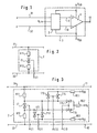
- Figure 1 shows an overall block diagram of an embodiment of a line receiver circuit.
- reference numeral 1 designates a differential input amplifier circuit having a non-inverting input terminal 11 and an inverting input terminal 12. A voltage difference across the input terminals 11 and 12 is amplified by the amplifier 1 in a linear or non-linear fashion and the amplified signal appears at output terminal 13 of the amplifier 1.
- Reference numeral 2 designates line termination impedance means connected across the input terminals 11 and 12 of amplifier 1.
- Conductors 31 and 32 constitute a transmission line which is driven by a data transmitter (not shown) and connected to the input terminals 11 and 12 of amplifier 1.
- the dashed box around input amplifier 1 and line termination impedance means 2 indicates that both the input amplifier circuit 1 as well as the line termination impedance means 2 are integrated on a common semiconductor substrate, i.e. that both the input amplifier 1 and the line termination impedance means 2 are components of the same integrated circuit.
- other elements can be provided on the integrated circuit, e.g. additional input amplifiers and line termination means for additional signal channels and other circuitry for processing the information received via each of the transmission lines connected to the integrated circuit.
- Terminals VDD and VSS in Figure 1 denote the power supply terminals for the input amplifier circuit 1. While the line termination impedance means 2 in Figure 1 is shown to receive a power supply voltage across VDD and VSS, such connection of the line termination impedance means 2 to VDD and VSS might not be necessary depending on the particular embodiment of the line termination impedance means 2.
- the line termination impedance means 2 is a resistor the resistance of which is selected in accordance with the characteristic impedance of transmission line 31, 32.
- the line termination impedance means 2 may also provide for common mode termination of each signal conductor with one termination impedance for each of the conductors 31 and 32 of the transmission line.
- the respective impedances are connected to VDD or VSS or to terminal VT, depending on the kind of termination expected by the transmitter. If each of the termination impedances is connected to the terminal VT, the application of an external voltage to this terminal enables a common mode termination of the conductors 31, 32 of the transmission line at an arbitrary potential which can be determined depending on the employed kind of transmitter.
- Figure 2 shows a first embodiment of line impedance termination means 2.
- line impedance termination means 2 comprises a series connection of a first impedance R11, a transmission gate T1 and a second impedance R12, this series connection being connected across the input terminals 11 and 12 of the input amplifier circuit 1.
- 31 and 32 denote the conductors of a symmetrical transmission line, (e.g. twisted pair or similar types of transmission lines), which is terminated by said series connection of R11, T1 and R12.
- impedances R11 and R12 preferably have the same impedance value.
- transmission gate T1 denotes a control terminal of transmission gate T1.
- transmission gate T1 takes a low impedance transmission state, i.e. connects impedances R11 and R12 substantially like a short circuit, or takes a high impedance blocking state, i.e. substantially disconnects R11 and R12.
- the first embodiment allows switching on or off the internal termination essentially constituted by R11 and R12 connected in series.
- the line receiver circuit according to this embodiment can be configured to operate on a dedicated transmission line or can be configured to operate on a data bus transmission line.
- the transmission gate is controlled to take the low impedance transmission state while in the latter case the transmission gate is controlled to take the high impedance blocking state.
- Figure 3 shows a second embodiment of a line termination impedance means. Similar to the embodiment depicted in Figure 2, also the second embodiment comprises a series connection of a first impedance R11, a transmission gate T1 and a second impedance R12, this series circuit being connected across the input terminals 11 and 12 of input amplifier 1. Reference numerals 31 and 32 again denote the conductors of a transmission line connected to the input terminals 11 and 12 of amplifier 1.
- the second embodiment comprises a first pair of transmission gates T11, T12, a second pair of transmission gates T13, T14 and a third pair of transmission gates T15, T16.
- C11 denotes a control terminal for controlling the transmission state of the transmission gates T11 and T12.
- C12 denotes a control terminal for controlling state of transmission gates T13 and T14
- C13 denotes a control terminal for controlling the transmission state of transmission gates T15 and T16.
- the transmission gates belonging to the same pair always take the same transmission state determined by the signal applied to the corresponding control terminal.
- the first transmission gate T11 of the first pair is connected between that terminal of impedance R12 which is connected to transmission gate T1, and the negative power supply terminal VSS.
- the second transmission gate T12 of the first pair is connected between that terminal R11 which is connected to transmission gate T1 and terminal VSS.
- the first transmission gate T13 of the second pair of transmission gates is connected to that terminal of impedance R12 which is connected to transmission gate T1 and the positive power supply VDD.
- the second transmission gate T14 of the second pair of transmission gates is connected between that terminal of impedance R11 which is connected with transmission gate T1 and power supply terminal VDD.
- the first transmission gate T15 of the third pair of transmission gates is connected between that terminal of impedance R11 that is connected to transmission gate T1, and a terminal VT for applying an external voltage potential.
- the second transmission gate T16 of the third pair is connected between that terminal of impedance R12 that is connected to transmission gate T1 and terminal VT.
- the second embodiment allows that the line impedance termination means can be configured to terminate a variety of different types of transmission lines. Depending on the control signals applied to control terminals C1, C11, C12 and C13, it is possible to configure the line receiver circuit incorporating the line termination impedance means of the second embodiment for terminating a symmetrical transmission line, and/or for providing a common mode termination of each of the conductors 31, 32 of the transmission line to the positive power supply potential VDD, or to the negative power supply potential VSS or to an arbitrary termination voltage applied to terminal VT. Also, this embodiment allows that no termination of the transmission line takes place at all.
- transmission gate T1 For terminating a symmetrical transmission line, transmission gate T1 is controlled to be in a low impedance transmission state while all other transmission gates depicted in Figure 3 are controlled to be in a high impedance blocking state.
- transmission gates T13 and T14 are controlled to take a low impedance transmission state while all other transmission gates depicted in Figure 3 are controlled to take a high impedance blocking state.
- transmission gates T11 and T12 are controlled to take a low impedance transmission state while all other transmission gates depicted in Figure 3 are controlled to take a high impedance blocking state.
- a voltage source providing an appropriate voltage level is connected between terminal VT and e.g. VSS, and all transmission gates except T15 and T16 are controlled to take a high impedance blocking state while T15 and T16 are controlled to take a low impedance transmission state.
- transmission gate T1 may be controlled to be in a low impedance transmission state and at the same time, in case that a common mode termination to VDD is desired, transmission gates T13 and T14 can be controlled to be in a low impedance transmission state.
- transmission gates T1, T15 and T16 are controlled to take a low impedance transmission state while all other transmission gates are in a blocking state.
- transmission gates T1, T11 and T12 are in a low impedance state while all other transmission gates are in a blocking state.
- an additional impedance RS1, RS2, RS3 can be provided acting as source impedance for the common mode termination voltage, as shown in Fig. 3.
- an Y-type termination of transmission lines 31 and 32 can also be obtained with transmission gate T1 being in a blocking state.
- transmission gates T11 to T16 would have to be higher, and accordingly, the size of these transmission gates would have to be larger than in the case, that for a Y-type termination also transmission gate T1 is controlled to take a low impedance transmission state.
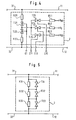
- Fig. 4 depicts a third embodiment of a line termination impedance means. This embodiment differs from the embodiment shown in Fig. 3 in that instead of a single transmission gate T1 connected between impedances R11 and R12, a series connection of two transmission gates T21 and T22 is connected between impedances R21 and R22. Moreover, in place of the pair of transmission gates T11, T12 a single transmission gate T25 is provided. In place of a pair of transmission gates T13, T14 a single transmission gate T23 is provided. In place of a pair of transmission gates T15, T16 a single transmission gate T24 is provided.
- Each of transmission gates T23 to T25 has one of its transmission terminals connected to that transmission terminal of T21 which is connected to a transmission terminal of T22, as shown in the figure. Operation and control of the third embodiment are similar to what has been described with regard to the second embodiment.
- both the impedances R11, R12, R21 and R22 and the impedances RS1, RS2, RS3 need not be present as separate components on the semiconductor chip but can be effected by means of designing the respective transmission gates such that in their respective low impedance transmission states they have a desired transmission impedance.
- the desired transmission impedance can e.g. be obtained by suitably designing the channel geometry.
- Fig. 5 shows an embodiment of a line termination impedance means according to the present invention.
- a series connection of three impedances R31, R32 and R33 is provided .
- Each of these impedances has a transmission gate T31, T32 and T33, respectively, connected in parallel.
- the control terminals of T31 to T33 are not shown in Fig. 5.
- This embodiment allows adjusting the line termination impedance between conductors 31 and 32 of the transmission line by means of shorting out selected impedances among the plurality of impedances R31 to R33 connected in series.
- additional transmission gates may be provided between amplifier input terminal 11 and said series connection and between amplifier input terminal 12 and said series connection, in order to allow for disconnection of the entire line termination impedance means 2 if desired.
- a modification of the line impedance termination means of Fig. 5 has the central transmission gate T32 replaced by a line termination impedance circuit 2 shown in Fig. 3 or by a line termination impedance circuit shown in Fig. 4.
- Control terminals C1 and C11, C12, C13 of each line impedance termination means 2 can be embodied as input configuration pins of the integrated circuit including the line receiver circuit of the present invention.
- a logic circuit can be provided for driving control terminals C1, C11, C12, C13 depending on the logical state of input terminals of the logic circuit such that erroneous combinations of transmission states of the transmission gates of the respective pairs of transmission gates are excluded. In this way, the number of configuration pins required for setting up the line termination impedance means 2 can be reduced and a destruction of the integrated circuit due to malconfiguration can be avoided.
- This logic circuit can also control said additional transmission gates not shown in the Figures, if provided.
- the logic circuit may receive binary information on the termination value and binary information on the termination type.
- Termination types may include no termination, i.e. very high termination impedance values approximating infinity, floating parallel (symmetrical) termination, common mode termination to VSS, VT or VDD and Y-termination to VSS, VT or VDD.
- a control circuit can be provided for actively adjusting the termination impedance to a desired value, to compensate for processing variations and/or temperature variations and/or power supply variations.
- the active control circuit may include an external reference resistor.
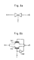
- Figure 6a shows the symbol used for depicting a transmission gate of the present invention.
- a transmission gate comprises two transmission terminals a, b as well as a control terminal c. Depending on the signal applied to control terminal c, with respect to terminals a and b the transmission gate takes a low impedance transmission state or a high impedance blocking state.
- Figure 6b shows an embodiment of the transmission gate of Figure 6a.
- the transmission gate comprises an NMOS transistor TR1 as well as a PMOS transistor TR2, the channels of the NMOS transistor TR1 and the PMOS transistor TR2 being connected in parallel between terminals a and b of the transmission gate.
- INV denotes an inverter the output of which is connected with the gate of PMOS transistor TR2.
- a control voltage at terminal c is applied to the gate of NMOS transistor TR1 as well as to the input of inverter INV.
- NMOS transistor TR1 is in a nonconducting state as long as neither the potential of terminal a nor the potential of terminal b is lower than the potential of terminal c minus the threshold voltage of TR1.
- the gate of PMOS transistor TR2 is at high potential (on or close to VDD) due to the action of inverter INV, such that also this transistor TR2 will be in a non-conducting state as long as neither the potential of terminal a nor the potential of terminal b rises above the gate potential of TR2 plus the threshold voltage of TR2. Accordingly, if terminal c is kept low the circuit depicted in Figure 6b will maintain a non-conducting high impedance state between terminals a and b as long as the potentials of terminals a and b remain within the limits just mentioned.
- NMOS transistor TR1 If the potential at terminal c is raised up to VDD or close to VDD, the gate of NMOS transistor TR1 receives high potential while due to the inverter INV the gate of PMOS transistor TR2 receives low voltage. Accordingly, NMOS transistor TR1 will conduct as long as that terminal of terminals a, b which has the lower potential, has a potential lower than the potential at control terminal c by the threshold voltage of TR1. PMOS transistor TR2 takes a conducting state as long as the higher potential of the potentials at terminals a, b is by the threshold voltage of TR2 higher than the gate voltage of PMOS transistor TR2 which is at or close to VSS.
Landscapes
- Engineering & Computer Science (AREA)
- Power Engineering (AREA)
- Computer Networks & Wireless Communication (AREA)
- Signal Processing (AREA)
- Logic Circuits (AREA)
- Dc Digital Transmission (AREA)
- Communication Control (AREA)
- Cable Transmission Systems, Equalization Of Radio And Reduction Of Echo (AREA)
- Amplifiers (AREA)
- Switches That Are Operated By Magnetic Or Electric Fields (AREA)
- Keying Circuit Devices (AREA)
Abstract
Description
- Figure 1
- shows an overall block diagram of a line receiver circuit.
- Figure 2
- shows a first embodiment of a line termination impedance means;
- Figure 3
- shows a second embodiment of a line termination impedance means ;
- Figure 4
- shows a third embodiment of a line termination impedance means ;
- Figure 5
- shows an embodiment of a line termination impedance means according to the present invention;
- Figure 6a
- shows the symbol used for depicting a transmission gate; and
- Figure 6b
- shows a schematic diagram of an embodiment of a transmission gate according to the invention.
Claims (2)
- Line receiver circuit, comprising
an integrated input amplifier circuit (1) having a non-inverting input terminal (11) and an inverting input terminal (12) for connection with a transmission line (31, 32);
line termination impedance means (2) connected between said inverting input terminal (12) and said non-inverting input terminal (11) for terminating the characteristic impedance of said transmission line (31, 32);
wherein the input amplifier circuit (1) and said line termination impedance means (2) are integrated on a common semiconductor substrate;
characterized by
said line termination impedance means (2) comprising a series connection of a plurality of impedances (R31, R32, R33);
at least one of said impedances (R31, R32, R33) having a transmission gate (T31, T32, T33) connected in parallel, said transmission gate being controllable to be in a low impedance transmission state or in a high impedance blocking state;
each transmission gate comprising a parallel connection of an N-channel MOSFET (TR1) and a P-channel MOSFET (TR2);
the gate of said N-channel MOSFET (TR1) being connected to receive a transmission control signal (C) and the gate of said P-channel MOSFET (TR2) being connected to receive said inverted transmission control signal, the transmission control signal (C) being selected so as to set the transmission gate in its transmission state or in its blocking state, to thereby select an appropriate level of the overall termination impedance. - Line receiver circuit according to claim 1, comprising
a plurality of line termination impedance means (2) connected in parallel between said input terminals (11, 12) of said input amplifier circuit (1).
Applications Claiming Priority (3)
| Application Number | Priority Date | Filing Date | Title |
|---|---|---|---|
| DE19618527 | 1996-05-08 | ||
| DE19618527A DE19618527A1 (en) | 1996-05-08 | 1996-05-08 | Line receiver circuit |
| PCT/EP1997/002351 WO1997042739A1 (en) | 1996-05-08 | 1997-05-07 | Integrated and switchable line termination |
Publications (2)
| Publication Number | Publication Date |
|---|---|
| EP0897629A1 EP0897629A1 (en) | 1999-02-24 |
| EP0897629B1 true EP0897629B1 (en) | 2005-09-07 |
Family
ID=7793728
Family Applications (1)
| Application Number | Title | Priority Date | Filing Date |
|---|---|---|---|
| EP97923014A Expired - Lifetime EP0897629B1 (en) | 1996-05-08 | 1997-05-07 | Integrated and switchable line termination |
Country Status (10)
| Country | Link |
|---|---|
| EP (1) | EP0897629B1 (en) |
| JP (1) | JP2000509586A (en) |
| CN (1) | CN1105442C (en) |
| AT (1) | ATE304263T1 (en) |
| AU (1) | AU2893997A (en) |
| CA (1) | CA2252746A1 (en) |
| DE (2) | DE19618527A1 (en) |
| HK (1) | HK1017536A1 (en) |
| TW (1) | TW361018B (en) |
| WO (1) | WO1997042739A1 (en) |
Families Citing this family (4)
| Publication number | Priority date | Publication date | Assignee | Title |
|---|---|---|---|---|
| DE19856283A1 (en) * | 1998-12-07 | 2000-06-08 | Bosch Gmbh Robert | Damping circuit for two-wire bus system |
| DE10211834A1 (en) * | 2002-03-16 | 2003-09-25 | Philips Intellectual Property | Vehicle data network, has line terminated by voltage-limiting nonlinear component such as Zener diode that has low resistance value above and/or below working range of data network |
| ES2373771T3 (en) | 2009-08-05 | 2012-02-08 | Nestec S.A. | CAPSULE WITH SEALING ELEMENT IN THE FORM OF RELIEF. |
| TWI469510B (en) * | 2012-10-09 | 2015-01-11 | Novatek Microelectronics Corp | Interface circuit |
Family Cites Families (6)
| Publication number | Priority date | Publication date | Assignee | Title |
|---|---|---|---|---|
| US5396028A (en) * | 1993-05-05 | 1995-03-07 | Texas Instruments Incorporated | Method and apparatus for transmission line termination |
| DE69419844T2 (en) * | 1993-06-18 | 2000-03-16 | Digital Equipment Corp | Integrated system bus interface architecture with precision receiver compensated for temperature, power supply and semiconductor manufacturing fluctuations |
| JPH07135513A (en) * | 1993-09-17 | 1995-05-23 | Fujitsu Ltd | Method and device for termination control for current drive circuit |
| SE9400657D0 (en) * | 1994-02-25 | 1994-02-25 | Ellemtel Utvecklings Ab | One, a control voltage generating, circuit |
| US5528168A (en) * | 1995-03-29 | 1996-06-18 | Intel Corporation | Power saving terminated bus |
| US5530377A (en) * | 1995-07-05 | 1996-06-25 | International Business Machines Corporation | Method and apparatus for active termination of a line driver/receiver |
-
1996
- 1996-05-08 DE DE19618527A patent/DE19618527A1/en not_active Withdrawn
-
1997
- 1997-05-07 AT AT97923014T patent/ATE304263T1/en not_active IP Right Cessation
- 1997-05-07 JP JP09539549A patent/JP2000509586A/en active Pending
- 1997-05-07 WO PCT/EP1997/002351 patent/WO1997042739A1/en active IP Right Grant
- 1997-05-07 EP EP97923014A patent/EP0897629B1/en not_active Expired - Lifetime
- 1997-05-07 AU AU28939/97A patent/AU2893997A/en not_active Abandoned
- 1997-05-07 CN CN97196088A patent/CN1105442C/en not_active Expired - Lifetime
- 1997-05-07 CA CA002252746A patent/CA2252746A1/en not_active Abandoned
- 1997-05-07 DE DE69734154T patent/DE69734154T2/en not_active Expired - Lifetime
- 1997-05-07 TW TW086106074A patent/TW361018B/en not_active IP Right Cessation
-
1999
- 1999-05-24 HK HK99102298A patent/HK1017536A1/en not_active IP Right Cessation
Also Published As
| Publication number | Publication date |
|---|---|
| DE69734154T2 (en) | 2006-06-29 |
| ATE304263T1 (en) | 2005-09-15 |
| CA2252746A1 (en) | 1997-11-13 |
| HK1017536A1 (en) | 1999-11-19 |
| EP0897629A1 (en) | 1999-02-24 |
| CN1105442C (en) | 2003-04-09 |
| CN1224556A (en) | 1999-07-28 |
| JP2000509586A (en) | 2000-07-25 |
| WO1997042739A1 (en) | 1997-11-13 |
| TW361018B (en) | 1999-06-11 |
| DE69734154D1 (en) | 2005-10-13 |
| AU2893997A (en) | 1997-11-26 |
| DE19618527A1 (en) | 1998-12-24 |
Similar Documents
| Publication | Publication Date | Title |
|---|---|---|
| US6037798A (en) | Line receiver circuit having termination impedances with transmission gates connected in parallel | |
| US7038498B2 (en) | Input/output circuit, reference-voltage generating circuit, and semiconductor integrated circuit | |
| US6690191B2 (en) | Bi-directional output buffer | |
| US7046041B1 (en) | Structures and methods of implementing a pass gate multiplexer with pseudo-differential input signals | |
| EP1316146B1 (en) | Circuit for producing low-voltage differential signals | |
| KR100381987B1 (en) | Binary weighted reference circuit for a variable impedance output buffer | |
| US7940086B2 (en) | Interface circuit that can switch between single-ended transmission and differential transmission | |
| US4772812A (en) | Tri-state output buffer circuit including a capacitor and dynamic depletion mode switching device | |
| US20020053923A1 (en) | Programmable termination circuit and method | |
| US6911860B1 (en) | On/off reference voltage switch for multiple I/O standards | |
| US5045730A (en) | Electrical circuitry providing compatibility between different logic levels | |
| GB2317515A (en) | Binary data link with reduced termination resistor dissipation | |
| US5994921A (en) | Universal sender device | |
| US5548229A (en) | Tri-state output buffer circuit | |
| US7400164B2 (en) | Integrated circuit and method of improving signal integrity | |
| US5828233A (en) | Mixed mode CMOS input buffer with bus hold | |
| EP0897629B1 (en) | Integrated and switchable line termination | |
| US4425517A (en) | Fail soft tri-state logic circuit | |
| US6239619B1 (en) | Method and apparatus for dynamic termination logic of data buses | |
| KR100462437B1 (en) | Line receiver circuit | |
| JPH11154859A (en) | Method and system for transmitting multilevel signal and semiconductor integrated circuit | |
| US5132561A (en) | Switching of logic data signals | |
| US5982218A (en) | Input circuit provided in a semiconductor integrated circuit, used in high-speed small-amplitude signal transmission system | |
| US6541998B2 (en) | Active termination circuit with an enable/disable | |
| JPS63153645A (en) | Parity generating circuit |
Legal Events
| Date | Code | Title | Description |
|---|---|---|---|
| PUAI | Public reference made under article 153(3) epc to a published international application that has entered the european phase |
Free format text: ORIGINAL CODE: 0009012 |
|
| 17P | Request for examination filed |
Effective date: 19981021 |
|
| AK | Designated contracting states |
Kind code of ref document: A1 Designated state(s): AT DE FR GB IT SE |
|
| RTI1 | Title (correction) |
Free format text: INTEGRATED AND SWITCHABLE LINE TERMINATION |
|
| 17Q | First examination report despatched |
Effective date: 20040126 |
|
| RAP1 | Party data changed (applicant data changed or rights of an application transferred) |
Owner name: TELEFONAKTIEBOLAGET LM ERICSSON (PUBL) |
|
| GRAP | Despatch of communication of intention to grant a patent |
Free format text: ORIGINAL CODE: EPIDOSNIGR1 |
|
| GRAS | Grant fee paid |
Free format text: ORIGINAL CODE: EPIDOSNIGR3 |
|
| GRAA | (expected) grant |
Free format text: ORIGINAL CODE: 0009210 |
|
| AK | Designated contracting states |
Kind code of ref document: B1 Designated state(s): AT DE FR GB IT SE |
|
| PG25 | Lapsed in a contracting state [announced via postgrant information from national office to epo] |
Ref country code: IT Free format text: LAPSE BECAUSE OF FAILURE TO SUBMIT A TRANSLATION OF THE DESCRIPTION OR TO PAY THE FEE WITHIN THE PRESCRIBED TIME-LIMIT;WARNING: LAPSES OF ITALIAN PATENTS WITH EFFECTIVE DATE BEFORE 2007 MAY HAVE OCCURRED AT ANY TIME BEFORE 2007. THE CORRECT EFFECTIVE DATE MAY BE DIFFERENT FROM THE ONE RECORDED. Effective date: 20050907 Ref country code: AT Free format text: LAPSE BECAUSE OF FAILURE TO SUBMIT A TRANSLATION OF THE DESCRIPTION OR TO PAY THE FEE WITHIN THE PRESCRIBED TIME-LIMIT Effective date: 20050907 |
|
| REG | Reference to a national code |
Ref country code: GB Ref legal event code: FG4D |
|
| REF | Corresponds to: |
Ref document number: 69734154 Country of ref document: DE Date of ref document: 20051013 Kind code of ref document: P |
|
| PG25 | Lapsed in a contracting state [announced via postgrant information from national office to epo] |
Ref country code: SE Free format text: LAPSE BECAUSE OF FAILURE TO SUBMIT A TRANSLATION OF THE DESCRIPTION OR TO PAY THE FEE WITHIN THE PRESCRIBED TIME-LIMIT Effective date: 20051207 |
|
| REG | Reference to a national code |
Ref country code: HK Ref legal event code: GR Ref document number: 1017536 Country of ref document: HK |
|
| ET | Fr: translation filed | ||
| PLBE | No opposition filed within time limit |
Free format text: ORIGINAL CODE: 0009261 |
|
| STAA | Information on the status of an ep patent application or granted ep patent |
Free format text: STATUS: NO OPPOSITION FILED WITHIN TIME LIMIT |
|
| 26N | No opposition filed |
Effective date: 20060608 |
|
| REG | Reference to a national code |
Ref country code: FR Ref legal event code: PLFP Year of fee payment: 20 |
|
| PGFP | Annual fee paid to national office [announced via postgrant information from national office to epo] |
Ref country code: DE Payment date: 20160527 Year of fee payment: 20 Ref country code: GB Payment date: 20160527 Year of fee payment: 20 |
|
| PGFP | Annual fee paid to national office [announced via postgrant information from national office to epo] |
Ref country code: FR Payment date: 20160530 Year of fee payment: 20 |
|
| REG | Reference to a national code |
Ref country code: DE Ref legal event code: R071 Ref document number: 69734154 Country of ref document: DE |
|
| REG | Reference to a national code |
Ref country code: GB Ref legal event code: PE20 Expiry date: 20170506 |
|
| PG25 | Lapsed in a contracting state [announced via postgrant information from national office to epo] |
Ref country code: GB Free format text: LAPSE BECAUSE OF EXPIRATION OF PROTECTION Effective date: 20170506 |