EP0891649B1 - Dc power converter - Google Patents
Dc power converter Download PDFInfo
- Publication number
- EP0891649B1 EP0891649B1 EP97916513A EP97916513A EP0891649B1 EP 0891649 B1 EP0891649 B1 EP 0891649B1 EP 97916513 A EP97916513 A EP 97916513A EP 97916513 A EP97916513 A EP 97916513A EP 0891649 B1 EP0891649 B1 EP 0891649B1
- Authority
- EP
- European Patent Office
- Prior art keywords
- inverter
- inverters
- pulse
- control
- output
- Prior art date
- Legal status (The legal status is an assumption and is not a legal conclusion. Google has not performed a legal analysis and makes no representation as to the accuracy of the status listed.)
- Expired - Lifetime
Links
- 238000012544 monitoring process Methods 0.000 claims description 9
- 230000004044 response Effects 0.000 claims description 6
- 238000001514 detection method Methods 0.000 claims description 2
- 238000004804 winding Methods 0.000 description 9
- 238000010586 diagram Methods 0.000 description 5
- 238000000034 method Methods 0.000 description 4
- 230000008569 process Effects 0.000 description 4
- 239000003990 capacitor Substances 0.000 description 3
- 230000003111 delayed effect Effects 0.000 description 3
- 230000005540 biological transmission Effects 0.000 description 2
- 230000001419 dependent effect Effects 0.000 description 2
- 238000009499 grossing Methods 0.000 description 2
- 239000002245 particle Substances 0.000 description 2
- 230000008859 change Effects 0.000 description 1
- 238000004891 communication Methods 0.000 description 1
- 230000001447 compensatory effect Effects 0.000 description 1
- 238000007796 conventional method Methods 0.000 description 1
- 239000013078 crystal Substances 0.000 description 1
- 230000001934 delay Effects 0.000 description 1
- 238000013461 design Methods 0.000 description 1
- 238000005516 engineering process Methods 0.000 description 1
- 230000006870 function Effects 0.000 description 1
- 239000011159 matrix material Substances 0.000 description 1
- 238000012545 processing Methods 0.000 description 1
- 230000001681 protective effect Effects 0.000 description 1
- 230000009467 reduction Effects 0.000 description 1
- 238000011160 research Methods 0.000 description 1
- 239000004065 semiconductor Substances 0.000 description 1
- 230000001360 synchronised effect Effects 0.000 description 1
Images




Classifications
-
- H—ELECTRICITY
- H02—GENERATION; CONVERSION OR DISTRIBUTION OF ELECTRIC POWER
- H02M—APPARATUS FOR CONVERSION BETWEEN AC AND AC, BETWEEN AC AND DC, OR BETWEEN DC AND DC, AND FOR USE WITH MAINS OR SIMILAR POWER SUPPLY SYSTEMS; CONVERSION OF DC OR AC INPUT POWER INTO SURGE OUTPUT POWER; CONTROL OR REGULATION THEREOF
- H02M7/00—Conversion of AC power input into DC power output; Conversion of DC power input into AC power output
- H02M7/02—Conversion of AC power input into DC power output without possibility of reversal
- H02M7/04—Conversion of AC power input into DC power output without possibility of reversal by static converters
- H02M7/06—Conversion of AC power input into DC power output without possibility of reversal by static converters using discharge tubes without control electrode or semiconductor devices without control electrode
- H02M7/10—Conversion of AC power input into DC power output without possibility of reversal by static converters using discharge tubes without control electrode or semiconductor devices without control electrode arranged for operation in series, e.g. for multiplication of voltage
-
- H—ELECTRICITY
- H02—GENERATION; CONVERSION OR DISTRIBUTION OF ELECTRIC POWER
- H02M—APPARATUS FOR CONVERSION BETWEEN AC AND AC, BETWEEN AC AND DC, OR BETWEEN DC AND DC, AND FOR USE WITH MAINS OR SIMILAR POWER SUPPLY SYSTEMS; CONVERSION OF DC OR AC INPUT POWER INTO SURGE OUTPUT POWER; CONTROL OR REGULATION THEREOF
- H02M3/00—Conversion of DC power input into DC power output
- H02M3/22—Conversion of DC power input into DC power output with intermediate conversion into AC
- H02M3/24—Conversion of DC power input into DC power output with intermediate conversion into AC by static converters
- H02M3/28—Conversion of DC power input into DC power output with intermediate conversion into AC by static converters using discharge tubes with control electrode or semiconductor devices with control electrode to produce the intermediate AC
-
- H—ELECTRICITY
- H02—GENERATION; CONVERSION OR DISTRIBUTION OF ELECTRIC POWER
- H02M—APPARATUS FOR CONVERSION BETWEEN AC AND AC, BETWEEN AC AND DC, OR BETWEEN DC AND DC, AND FOR USE WITH MAINS OR SIMILAR POWER SUPPLY SYSTEMS; CONVERSION OF DC OR AC INPUT POWER INTO SURGE OUTPUT POWER; CONTROL OR REGULATION THEREOF
- H02M3/00—Conversion of DC power input into DC power output
- H02M3/22—Conversion of DC power input into DC power output with intermediate conversion into AC
- H02M3/24—Conversion of DC power input into DC power output with intermediate conversion into AC by static converters
- H02M3/28—Conversion of DC power input into DC power output with intermediate conversion into AC by static converters using discharge tubes with control electrode or semiconductor devices with control electrode to produce the intermediate AC
- H02M3/285—Single converters with a plurality of output stages connected in parallel
-
- H—ELECTRICITY
- H02—GENERATION; CONVERSION OR DISTRIBUTION OF ELECTRIC POWER
- H02M—APPARATUS FOR CONVERSION BETWEEN AC AND AC, BETWEEN AC AND DC, OR BETWEEN DC AND DC, AND FOR USE WITH MAINS OR SIMILAR POWER SUPPLY SYSTEMS; CONVERSION OF DC OR AC INPUT POWER INTO SURGE OUTPUT POWER; CONTROL OR REGULATION THEREOF
- H02M3/00—Conversion of DC power input into DC power output
- H02M3/22—Conversion of DC power input into DC power output with intermediate conversion into AC
- H02M3/24—Conversion of DC power input into DC power output with intermediate conversion into AC by static converters
- H02M3/28—Conversion of DC power input into DC power output with intermediate conversion into AC by static converters using discharge tubes with control electrode or semiconductor devices with control electrode to produce the intermediate AC
- H02M3/325—Conversion of DC power input into DC power output with intermediate conversion into AC by static converters using discharge tubes with control electrode or semiconductor devices with control electrode to produce the intermediate AC using devices of a triode or a transistor type requiring continuous application of a control signal
- H02M3/335—Conversion of DC power input into DC power output with intermediate conversion into AC by static converters using discharge tubes with control electrode or semiconductor devices with control electrode to produce the intermediate AC using devices of a triode or a transistor type requiring continuous application of a control signal using semiconductor devices only
- H02M3/337—Conversion of DC power input into DC power output with intermediate conversion into AC by static converters using discharge tubes with control electrode or semiconductor devices with control electrode to produce the intermediate AC using devices of a triode or a transistor type requiring continuous application of a control signal using semiconductor devices only in push-pull configuration
- H02M3/3376—Conversion of DC power input into DC power output with intermediate conversion into AC by static converters using discharge tubes with control electrode or semiconductor devices with control electrode to produce the intermediate AC using devices of a triode or a transistor type requiring continuous application of a control signal using semiconductor devices only in push-pull configuration with automatic control of output voltage or current
-
- Y—GENERAL TAGGING OF NEW TECHNOLOGICAL DEVELOPMENTS; GENERAL TAGGING OF CROSS-SECTIONAL TECHNOLOGIES SPANNING OVER SEVERAL SECTIONS OF THE IPC; TECHNICAL SUBJECTS COVERED BY FORMER USPC CROSS-REFERENCE ART COLLECTIONS [XRACs] AND DIGESTS
- Y02—TECHNOLOGIES OR APPLICATIONS FOR MITIGATION OR ADAPTATION AGAINST CLIMATE CHANGE
- Y02B—CLIMATE CHANGE MITIGATION TECHNOLOGIES RELATED TO BUILDINGS, e.g. HOUSING, HOUSE APPLIANCES OR RELATED END-USER APPLICATIONS
- Y02B70/00—Technologies for an efficient end-user side electric power management and consumption
- Y02B70/10—Technologies improving the efficiency by using switched-mode power supplies [SMPS], i.e. efficient power electronics conversion e.g. power factor correction or reduction of losses in power supplies or efficient standby modes
Definitions
- the present invention relates to a DC power converter which is suitable for producing high DC voltages.
- a klystron typically requires a 50kV DC power supply.
- a conventional DC converter used to power a klystron comprises an array of line-commutated rectifiers. With such an arrangement the output is a DC signal on which a relatively small amplitude AC ripple voltage is superimposed. It is necessary to remove this ripple by passing the converter output through a smoothing filter which incorporates an inductor and a capacitor. When the system is operating this inductor and capacitor store energy, typically of the order of tens of kilojoules. This is not normally a problem but should an internal arc occur in the klystron, the stored energy is released.
- Klystrons have a tendency to arc internally, particularly after long periods of being shut down. It is necessary to provide a fast-acting protection device to remove the high voltage generated by the stored energy in the event of an internal arc occurring. The device must remove the voltage in microseconds. This is conventionally achieved by using a fast-acting electronic "crowbar" protection device, generally in the form of a gas filled electronic tube. The power converter has to be designed to withstand frequent operations of the protection device which applies a near short circuit to the converter output. Thus the conventional techniques for dealing with internal arcing have significant implications with regard to cost and/or reliability.
- WO 86/04749 discloses a converter comprising the features of the preamble of claim 1.
- the rectified outputs may be connected in series, parallel or any other configuration suitable to a particular application.
- the modular nature of the system gives great flexibility in that standard sub-systems can be connected in different configurations appropriate to different applications. Furthermore, faulty sub-systems can be readily isolated and replaced.
- the invention provides a bank of relatively simple high frequency switch-mode inverters with their outputs combined to produce a very low ripple high voltage output requiring a minimum filter storing only a few joules, or even no filter at all if sufficient inverters are used. Furthermore the inverters can be switched off rapidly without delivering sufficient energy into a faulty load to cause damage, and the soft commutation characteristics of a resonant inverter as compared with a chopper type inverter make it easier to keep electromagnetic noise under control.
- This mode of operation may be achieved in accordance with the present invention by monitoring the operation of one or a master inverter, and controlling the operation of the other or slave inverters in synchronism with the operation of the master inverter such that the predetermined phase relationship is maintained.
- the direction of current through a reactive component of the master inverter is monitored, and a timing pulse is generated in response to detection of the reversal of the monitored current.
- Control pulses are then generated for controlling the operation of the inverters with each control pulse having a predetermined phase relationship to the timing pulse.
- the control pulse applied to the master inverter must be in phase with the timing pulse, and the control pulses applied to the slave inverters may be delayed with respect to the timing pulse by multiples of the period of the timing pulse divided by the total number of inverters.
- the period of the timing pulse may be monitored and the duration of the inverter control pulses set so as to produce the required power output from the inverter.
- Figure 1 shows a circuit diagram of a DC power converter according to the present invention for converting a 415V three phase AC supply to a 50kV DC supply for a klystron 1 of a particle accelerator (not shown).
- the power converter comprises a master inverter 2 and five slave inverters 2a.
- the six inverters 2, 2a (each including an AC to DC rectifier 3 (shown in Figure 2)) are arranged to operate in a sequence locked to the operation of the master inverter 2.
- the inverters 2, 2a each convert the rectified 415V AC to a high frequency AC output which is then stepped up by a respective transformer 4 and rectified to a DC voltage by a bridge rectifier 5.
- the final output voltage is indicated by V out and represents the sum of the voltages across the bridge rectifiers 5.
- the master inverter 2 is shown in detail in Figure 2, but all the six inverters are of the same resonant switch-mode type in which current is conducted alternately in one direction and the other through an inductor L and capacitor C, the direction of conduction being governed by the operation of insulated gate bipolar transistor (IGBT) switches T.
- IGBT insulated gate bipolar transistor
- the current I L in the inductor of each inverter 2,2a is thus cyclical and passes through zero once every half cycle when switching occurs.
- This waveform is processed by full bridge control electronics described in greater detail below to deliver a short (approximately two microseconds) pulse P Z at each zero crossing.
- the pulse P Z is used as the timing reference by digital control electronics shown in block form in Figure 2 to ensure that switching occurs in all the inverters in a timed relationship so that the resultant ripple in the output voltage V out is minimised.
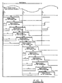
- the first waveform in Figure 3 is the current I sw fed into the resonant circuit by the switches T.
- the output voltage V M , V s1-s5 and current I M , I s1-s5 of each inverter 2, 2a is monitored by the digital control circuitry so that the required voltage and phase relationship can be established.
- the master inverter 2 of Figure 1 is shown with associated digital control circuitry (indicated generally by reference numeral 6) which is also connected to each of the slave inverters 2a.
- the output of the master inverter 2 governs the operation of the slave inverters 2a.
- the switching of each inverter 2, 2a is controlled by a respective switching control circuit 7 which is responsive to control signals received from the digital control circuitry 6.
- the switching control circuit 7 of each inverter 2, 2a generates a pulse when the current I n the inductor of its resonant circuit crosses zero. These pulses are transmitted to the digital control circuit 6.
- the pulse P Z is that generated by the master inverter 2.
- the resonant inverter circuit 2 shown in Figure 2 is of conventional form and its structure and mode of operation will not therefore be described in detail in this document. It will be appreciated however that its frequency of operation will be a function of output voltage and current that will in turn be dependent upon the load.
- the digital control circuit 6 comprises a fast digital signal processor 8 coupled to an external control system via, for example, a VME bus 9, a control signal generator 10 and a voltage and phase monitor circuit 11.
- the control signal generator 10 transmits control signals to the switching control circuit 7 of each inverter 2, 2a and receives the current zero crossing pulses P Z from the master inverter 2.
- the voltage and phase monitor circuit 11 receives signals from each inverter 2, 2a indicative of their output voltages V M , V S1 - V S5 , and their output currents I M , I S1 - I S5 .
- the control signal generator 10 comprises delay generation logic which is activated by receipt of the master inverter current zero crossing pulse P Z and which combine to produce a control pulse of a calculated time delay t (relative to the leading edge of the pulse P Z ) and width w for each inverter 2, 2a. This control pulse is then transmitted to the appropriate switching control circuit 7 so that switch-on of the IGBT's of the inverter 2, 2a occurs on the leading edge of the control pulse and switch-off occurs on the trailing edge.
- FIG 3 shows sets of control signal pulses generated in response to current zero crossing pulses P Z of the master inverter 2 for each half cycle of the master inverter output. It will be seen that each slave inverter 2a control pulse is delayed by a time T 1 - T 5 with respect to the zero crossing pulse P Z of the master inverter 2 and is of a duration that will deliver an output voltage equal to that delivered by the master inverter.
- the period of the master inverter waveform is shown as 40 ⁇ s. This period will vary as the circuitry responds to fluctuating operating condition and typically the period could range from 25 to 67 ⁇ s.
- Figure 3 shows successive "ON" control pulses for each half cycle of the inverters separately to simplify the illustration but it will be appreciated that in practice successive control pulses may be generated by a single circuit.
- Figure 4 shows in detail the control signal generator circuit 10 for each inverter 2, 2a. It comprises a group of four registers DHN, DCN, WHN and WCN, each being 12 bits long and therefore capable of storing numbers up to 4096. Registers DHN and WHN are respectively delay hold and width hold registers connected to the signal processor 8 via a data bus 13 and which respectively feed delay and width counting registers DCN and WCN. The control signal pulse is generated at the output of the width counting register WCN.
- the delay and width hold registers DHN and WHN are each loaded at any time with a number from the signal processor 8. These numbers are calculated by the signal processor 8 in response to information received from the outputs of the inverters 2, 2a and the demanded output voltage of the complete power converter.
- the number stored in delay hold register DHN is copied into delay counting register DCN. Provided this number is greater than zero, this number is decremented by one each time a pulse from a crystal controlled clock oscillator is received. Thus for a clock frequency of 100Mhz the register counts down in units of 10 nanoseconds.
- the width counting register WCN When the value in the delay counting register DCN reaches one, the width counting register WCN is loaded with the contents of width holding register WHN and its output changes from LOW to HIGH. The value in register WCN is then decremented in accordance with the clock pulse until the value reaches zero, whereupon its output reverts to LOW.
- the value in the delay hold register DHN governs the delay between the zero crossing pulse P Z of the master inverter 2 being detected and the output control pulse being generated, whereas the value in width hold register WHN governs the width w of that pulse.
- control pulses are generated by identical circuitry for each inverter 2, 2a.
- each inverter 2, 2a In order to control the phase of each inverter 2, 2a, the operating frequency of the master inverter 2 is monitored and the appropriate delay between the switching of each slave inverter 2a is calculated by the signal processor 8. The calculated delay value T 1 - T 5 for each inverter 2a is loaded into the appropriate delay hold register DHN for that inverter as described above. The actual switching delay T 1 - T 5 of each slave inverter 2a is monitored (as described below) and fed to the signal processor 8 which maintains the correct phase by closed loop control.
- a period counting register PCR and holding register PHR monitor the master inverter, and five holding registers PHN (only one of which is shown) monitor the slave inverters.
- the value present in the counting register PCR is continually incremented in response to a clock pulse and the count is made available to the period count holding registers PHR and all holding registers PHN via a private data bus.
- Counting is performed with reference to the receipt of the current zero crossing pulse P Z for the master inverter 2 and the current zero crossing pulses for the slave inverters 2a, each pulse being synchronised with the clock pulse by conventional circuitry.
- the contents of the period counting register PCR are copied to holding register PHR and a one is loaded into the reset counting register PCR to compensate for the loss of a clock count during the copying process.
- the value in counting register PCR is then continually incremented in response to the clock pulses until the next current zero crossing pulse P Z is received half a period later, whereupon the counter is reset again. It will be understood that the value present in holding register PHR at any time reflects the half period of the master inverter output current waveform I M .
- each hold register PHN will contain a value reflecting the delay in the zero crossing of the respective slave inverter with reference to the zero crossing of the master inverter.
- the values stored in each hold register PHR, PHN are made available for transmission to the signal processor 8 every half cycle of the master inverter 2. These values can be processed by the signal processor 8 to calculate the delay time T N required for each of the switching control signals.
- the voltage and phase monitoring circuit 11 receives the voltage output of a potential divider connected across the main output, and the voltage outputs V M , V S1 -V S5 of each inverter 2, 2a.
- Each of these analogue signals is converted to digital by an analogue to digital converter ADC (not shown).
- the output of each ADC is in serial form, is stored in a shift register (not shown), and is read out in parallel by the digital signal processor 8. If a slave inverter should fail, the voltage and phase of the remaining inverters can be re-optimised to continue running with reduced output and slightly greater ripple until it is convenient to shut down and replace it.
- Transmission of data from the holding registers to the digital signal processor 8 is achieved by using fast communication ports working in direct memory access mode. This enables the processor 8 to read the latest values of the inverter parameters without delay, enabling compensatory action to be taken where necessary.
- a fast overcurrent detector (not shown) is provided in the main output. In the event of an overcurrent being detected, the system is quickly shut down by removing an enable output signal from each of the bridge controls 7.
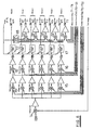
- FIG. 6 is a schematic representation of the feedback control loops and computational processes implemented in the described system.
- the total output voltage of the system as delivered to the load is compared with a "demanded" voltage represented by a voltage setpoint by a comparator 14.
- the resultant "difference" output is amplified to provide a signal representing a voltage demand for each of the six inverters and that signal is applied to each of the six comparators 15 which also receive respective voltage outputs V M , V S1 - V S5 from the inverters.
- the outputs of the comparators 15 are amplified to provide signals representing current demand signals for each inverter, and those signals are applied to respective comparators 16.
- the comparators 16 also receive the respective inverter current signals I M , I S1 - I S5 .
- the outputs of the comparators 16 are amplified to provide signals representing duty cycle demand signals for each inverter.
- the amplified outputs of the comparators 16 and a signal representing the period of the pulse P Z are used as the basis of the computation represented by boxes 17 which compute a pulse width for each inverter.
- the pulse period signal is also used to compute a delay setpoint for each of the slave inverters in a process represented by box 18, the delay setpoints being compared with the actual slave inverter delays T 1 - T 5 to generate a signal which is amplified to provide the required pulse delay signals for the slave inverters.
- the power converter design may be modular in nature and can be adapted to different numbers of inverters according to the power output required.
- the rectified outputs are connected in series to provide a high voltage output at a modest current. It is equally possible to produce a high current, low voltage power converter with low inherent ripple by connecting the rectifier outputs in parallel.
- Other alternatives include for example combining the outputs in a series/parallel matrix, or providing three inverters with phases of 0°, 120° and 240° with each inverter feeding a respective winding of a three phase transformer and the outputs of the transformer being applied to a three phase bridge rectifier.
- FIG 1 shows a circuit in which each inverter is coupled to a transformer 4 having a single output winding connected to a single rectifier bridge.
- the circuit components shown in Figure 7 are capable of producing a 4 amp output at a voltage of 12kV. Typically an assembly of eight such circuits would be provided in a four in series, two in parallel, array to generate an 8 amp output at a voltage of 48kV.
- a first inverter (not shown) drives an input winding 19 of a transformer 20 having three output windings 21. Each output winding is connected to a respective bridge recitifier 22.
- a second inverter (not shown) drives an input winding 23 of a transformer 24 having three output windings 25. Each output winding 25 is connected to a respective bridge rectifier 26.
- the second inverter is phase shifted by 90° relative to the first, and the rectifiers 22, 26 are connected together in pairs. Small filters formed by components 27, 28 ensure a smooth DC output of 4kV from each of the three rectifier pairs.
Landscapes
- Engineering & Computer Science (AREA)
- Power Engineering (AREA)
- Inverter Devices (AREA)
Description
Claims (4)
- A DC power converter comprising a plurality of resonant inverters (2, 2a) each generating an AC output which is applied to a respective transformer (4), a rectifier circuit (5) for rectifying the outputs of the transformers (4) and combining the rectified outputs, a controller (7) for monitoring the outputs of each of the inverters and generating signals to control the phase of each of the inverters (2, 2a) such that a regular predetermined phase relationship is maintained between the inverters which maintain a stable DC output, characterized by means (6) for monitoring the operation of one inverter (2), and means for controlling the operation of the other inverters (2a) in synchronism with the operation of the said one inverter such that the predetermined phase relationship is maintained.
- A DC power converter according to claim 1, wherein the rectified outputs are combined in series.
- A DC power converter according to claim 1 or 2, comprising means for monitoring the direction of current in a reactive component of the said one inverter, means for generating a timing pulse in response to detection of the reversal of the direction of the monitored current, and means for generating control pulses for controlling the operation of the inverters, each control pulse having a predetermined phase relationship to the timing pulse.
- A DC power converter according to claim 3, wherein each control pulse which is applied to one of the said other inverters is out of phase with the timing pulse by a multiple of the period of the timing pulse divided by the total number of inverters.
Applications Claiming Priority (3)
| Application Number | Priority Date | Filing Date | Title |
|---|---|---|---|
| GBGB9607381.2A GB9607381D0 (en) | 1996-04-04 | 1996-04-04 | Dc power converter |
| GB9607381 | 1996-04-04 | ||
| PCT/GB1997/000947 WO1997038479A1 (en) | 1996-04-04 | 1997-04-03 | Dc power converter |
Publications (2)
| Publication Number | Publication Date |
|---|---|
| EP0891649A1 EP0891649A1 (en) | 1999-01-20 |
| EP0891649B1 true EP0891649B1 (en) | 2002-12-18 |
Family
ID=10791783
Family Applications (1)
| Application Number | Title | Priority Date | Filing Date |
|---|---|---|---|
| EP97916513A Expired - Lifetime EP0891649B1 (en) | 1996-04-04 | 1997-04-03 | Dc power converter |
Country Status (5)
| Country | Link |
|---|---|
| EP (1) | EP0891649B1 (en) |
| AU (1) | AU2513697A (en) |
| DE (1) | DE69717979D1 (en) |
| GB (1) | GB9607381D0 (en) |
| WO (1) | WO1997038479A1 (en) |
Cited By (2)
| Publication number | Priority date | Publication date | Assignee | Title |
|---|---|---|---|---|
| FR2914685A1 (en) * | 2007-04-05 | 2008-10-10 | Renault Sas | ELECTRIC POWER SUPPLY SYSTEM OF A PLASMA DEPOLLUTION DEVICE FOR MOUNTING ON A MOTOR VEHICLE |
| CN100517935C (en) * | 2006-12-26 | 2009-07-22 | 中国电子科技集团公司第十四研究所 | Integrated device of transformer and voltage doubler rectifier circuit |
Families Citing this family (33)
| Publication number | Priority date | Publication date | Assignee | Title |
|---|---|---|---|---|
| US6160725A (en) * | 1999-03-12 | 2000-12-12 | Nmb Usa Inc. | System and method using phase detection to equalize power from multiple power sources |
| US6738275B1 (en) | 1999-11-10 | 2004-05-18 | Electromed Internationale Ltee. | High-voltage x-ray generator |
| EP2605393A3 (en) * | 1999-11-10 | 2014-08-13 | EMD Technologies, Inc. | High-voltage X-ray generator |
| US8571179B2 (en) | 1999-11-10 | 2013-10-29 | Robert Beland | Computed tomography systems |
| US7615893B2 (en) * | 2000-05-11 | 2009-11-10 | Cameron International Corporation | Electric control and supply system |
| DE20115473U1 (en) * | 2001-09-19 | 2003-02-20 | Biester, Klaus, 29342 Wienhausen | Universal energy supply system |
| DE20115474U1 (en) | 2001-09-19 | 2003-02-20 | Biester, Klaus, 29342 Wienhausen | DC converter device |
| DE20018560U1 (en) | 2000-10-30 | 2002-03-21 | CAMERON GmbH, 29227 Celle | Control and supply system |
| DE20115471U1 (en) | 2001-09-19 | 2003-02-20 | Biester, Klaus, 29342 Wienhausen | Universal energy supply system |
| BR0200298A (en) | 2001-02-05 | 2002-10-29 | Faiveley Transport | Power converter |
| FR2825847B1 (en) * | 2001-06-12 | 2003-09-12 | Faiveley Transport | ELECTRONIC CONNECTION CIRCUIT IN SERIES AND / OR PARALLEL OF GENERATORS |
| FR2820562B1 (en) * | 2001-02-05 | 2003-04-11 | Faiveley Transport | ELECTRONIC CONNECTION CIRCUIT IN SERIES AND / OR PARALLEL OF GENERATORS |
| FR2820561A1 (en) * | 2001-02-05 | 2002-08-09 | Faiveley Transport | AC/DC electrical energy conversion circuit uses a group of series and/or parallel connected transformers with controlled switched primary and rectified secondary circuits |
| US8710765B2 (en) | 2010-05-08 | 2014-04-29 | Robert Beland | LED illumination systems |
| EP1845755A3 (en) | 2006-04-10 | 2014-04-02 | EMD Technologies, Inc. | Illumination systems |
| GB2449427B (en) | 2007-05-19 | 2012-09-26 | Converteam Technology Ltd | Control methods for the synchronisation and phase shift of the pulse width modulation (PWM) strategy of power converters |
| US10892140B2 (en) | 2018-07-27 | 2021-01-12 | Eagle Harbor Technologies, Inc. | Nanosecond pulser bias compensation |
| US10978955B2 (en) | 2014-02-28 | 2021-04-13 | Eagle Harbor Technologies, Inc. | Nanosecond pulser bias compensation |
| US11004660B2 (en) | 2018-11-30 | 2021-05-11 | Eagle Harbor Technologies, Inc. | Variable output impedance RF generator |
| US11430635B2 (en) | 2018-07-27 | 2022-08-30 | Eagle Harbor Technologies, Inc. | Precise plasma control system |
| GB2551824A (en) * | 2016-06-30 | 2018-01-03 | Univ Nottingham | High frequency high power converter system |
| EP3665775B1 (en) | 2017-08-25 | 2025-08-20 | Eagle Harbor Technologies, Inc. | Arbitrary waveform generation using nanosecond pulses |
| US11532457B2 (en) | 2018-07-27 | 2022-12-20 | Eagle Harbor Technologies, Inc. | Precise plasma control system |
| US11222767B2 (en) | 2018-07-27 | 2022-01-11 | Eagle Harbor Technologies, Inc. | Nanosecond pulser bias compensation |
| US11810761B2 (en) | 2018-07-27 | 2023-11-07 | Eagle Harbor Technologies, Inc. | Nanosecond pulser ADC system |
| KR102499709B1 (en) | 2018-08-10 | 2023-02-16 | 이글 하버 테크놀로지스, 인코포레이티드 | Plasma sheath control for RF plasma reactors |
| US12456604B2 (en) | 2019-12-24 | 2025-10-28 | Eagle Harbor Technologies, Inc. | Nanosecond pulser RF isolation for plasma systems |
| EP3977616A4 (en) * | 2019-05-24 | 2023-06-14 | Eagle Harbor Technologies, Inc. | Klystron driver |
| TWI778449B (en) | 2019-11-15 | 2022-09-21 | 美商鷹港科技股份有限公司 | High voltage pulsing circuit |
| KR20230150396A (en) | 2019-12-24 | 2023-10-30 | 이글 하버 테크놀로지스, 인코포레이티드 | Nanosecond pulser rf isolation for plasma systems |
| US11967484B2 (en) | 2020-07-09 | 2024-04-23 | Eagle Harbor Technologies, Inc. | Ion current droop compensation |
| US11824542B1 (en) | 2022-06-29 | 2023-11-21 | Eagle Harbor Technologies, Inc. | Bipolar high voltage pulser |
| CN119998919A (en) | 2022-09-29 | 2025-05-13 | 鹰港科技有限公司 | High pressure plasma control |
Family Cites Families (4)
| Publication number | Priority date | Publication date | Assignee | Title |
|---|---|---|---|---|
| US3832622A (en) * | 1973-07-11 | 1974-08-27 | Avionic Instr Inc | Parallel phase lock circuitry for inverters and the like |
| US4695933A (en) * | 1985-02-11 | 1987-09-22 | Sundstrand Corporation | Multiphase DC-DC series-resonant converter |
| FR2633115B1 (en) * | 1988-06-17 | 1993-02-12 | Gen Electric Cgr | STABILIZED POWER SUPPLY WITH REDUCED ROPE RATE |
| US5418707A (en) * | 1992-04-13 | 1995-05-23 | The United States Of America As Represented By The United States Department Of Energy | High voltage dc-dc converter with dynamic voltage regulation and decoupling during load-generated arcs |
-
1996
- 1996-04-04 GB GBGB9607381.2A patent/GB9607381D0/en active Pending
-
1997
- 1997-04-03 WO PCT/GB1997/000947 patent/WO1997038479A1/en not_active Ceased
- 1997-04-03 DE DE69717979T patent/DE69717979D1/en not_active Expired - Lifetime
- 1997-04-03 AU AU25136/97A patent/AU2513697A/en not_active Abandoned
- 1997-04-03 EP EP97916513A patent/EP0891649B1/en not_active Expired - Lifetime
Cited By (3)
| Publication number | Priority date | Publication date | Assignee | Title |
|---|---|---|---|---|
| CN100517935C (en) * | 2006-12-26 | 2009-07-22 | 中国电子科技集团公司第十四研究所 | Integrated device of transformer and voltage doubler rectifier circuit |
| FR2914685A1 (en) * | 2007-04-05 | 2008-10-10 | Renault Sas | ELECTRIC POWER SUPPLY SYSTEM OF A PLASMA DEPOLLUTION DEVICE FOR MOUNTING ON A MOTOR VEHICLE |
| WO2008139087A3 (en) * | 2007-04-05 | 2009-02-19 | Renault Sa | Power supply system for a plasma pollution control device to be mounted on an automobile |
Also Published As
| Publication number | Publication date |
|---|---|
| EP0891649A1 (en) | 1999-01-20 |
| GB9607381D0 (en) | 1996-06-12 |
| AU2513697A (en) | 1997-10-29 |
| WO1997038479A1 (en) | 1997-10-16 |
| DE69717979D1 (en) | 2003-01-30 |
Similar Documents
| Publication | Publication Date | Title |
|---|---|---|
| WO1997038479A1 (en) | Dc power converter | |
| KR101205279B1 (en) | Method and apparatus for converting direct current to alternating current | |
| EP0851567B1 (en) | Multiparalleling system of voltage source power converters | |
| US4730242A (en) | Static power conversion and apparatus having essentially zero switching losses | |
| EP3240174B1 (en) | System and method for operating a power converter | |
| EP2214301B1 (en) | Power conversion systems and methods for controlling harmonic distortion | |
| CA2689503C (en) | Prediction scheme for step wave power converter and inductive inverter topology | |
| US7428158B2 (en) | System and method for reducing harmonic effects on a power delivery system | |
| US5450306A (en) | Closed loop pulse width modulator inverter with volt-seconds feedback control | |
| US5719759A (en) | DC/AC converter with equally loaded switches | |
| JPH0638696B2 (en) | Power converter | |
| US6144191A (en) | Voltage regulator | |
| EP1450476B1 (en) | Power converter circuit | |
| CN119182272A (en) | Device for current sharing of parallel-connected converters | |
| GB2350244A (en) | Voltage converter | |
| US20210297000A1 (en) | Dc-to-dc converter and operation thereof | |
| US12438445B2 (en) | Method, system, and apparatus for power conversion | |
| JPH11233298A (en) | Power supply and particle accelerator | |
| Prasai et al. | Zero-energy sag corrector with reduced device count | |
| GB2051507A (en) | Selective commutation circuit for an inverter | |
| Backman et al. | Modern circuit topology enables compact power factor corrected three-phase rectifier module | |
| Benedetti et al. | New high-performance thyristor gate control set for line-commutated converters | |
| Loh et al. | A time-based double band hysteresis current regulation strategy for single-phase multilevel inverters | |
| JP2830619B2 (en) | Static var compensator | |
| Tsai et al. | Interleaving control schemes for critical-mode boost PFC |
Legal Events
| Date | Code | Title | Description |
|---|---|---|---|
| PUAI | Public reference made under article 153(3) epc to a published international application that has entered the european phase |
Free format text: ORIGINAL CODE: 0009012 |
|
| 17P | Request for examination filed |
Effective date: 19981016 |
|
| AK | Designated contracting states |
Kind code of ref document: A1 Designated state(s): DE FR NL |
|
| GRAG | Despatch of communication of intention to grant |
Free format text: ORIGINAL CODE: EPIDOS AGRA |
|
| 17Q | First examination report despatched |
Effective date: 20011219 |
|
| GRAG | Despatch of communication of intention to grant |
Free format text: ORIGINAL CODE: EPIDOS AGRA |
|
| GRAH | Despatch of communication of intention to grant a patent |
Free format text: ORIGINAL CODE: EPIDOS IGRA |
|
| GRAH | Despatch of communication of intention to grant a patent |
Free format text: ORIGINAL CODE: EPIDOS IGRA |
|
| GRAA | (expected) grant |
Free format text: ORIGINAL CODE: 0009210 |
|
| AK | Designated contracting states |
Kind code of ref document: B1 Designated state(s): DE FR NL |
|
| PG25 | Lapsed in a contracting state [announced via postgrant information from national office to epo] |
Ref country code: NL Free format text: LAPSE BECAUSE OF FAILURE TO SUBMIT A TRANSLATION OF THE DESCRIPTION OR TO PAY THE FEE WITHIN THE PRESCRIBED TIME-LIMIT Effective date: 20021218 Ref country code: FR Free format text: LAPSE BECAUSE OF FAILURE TO SUBMIT A TRANSLATION OF THE DESCRIPTION OR TO PAY THE FEE WITHIN THE PRESCRIBED TIME-LIMIT Effective date: 20021218 |
|
| REF | Corresponds to: |
Ref document number: 69717979 Country of ref document: DE Date of ref document: 20030130 Kind code of ref document: P Ref document number: 69717979 Country of ref document: DE Date of ref document: 20030130 |
|
| PG25 | Lapsed in a contracting state [announced via postgrant information from national office to epo] |
Ref country code: DE Free format text: LAPSE BECAUSE OF FAILURE TO SUBMIT A TRANSLATION OF THE DESCRIPTION OR TO PAY THE FEE WITHIN THE PRESCRIBED TIME-LIMIT Effective date: 20030319 |
|
| PLBE | No opposition filed within time limit |
Free format text: ORIGINAL CODE: 0009261 |
|
| STAA | Information on the status of an ep patent application or granted ep patent |
Free format text: STATUS: NO OPPOSITION FILED WITHIN TIME LIMIT |
|
| EN | Fr: translation not filed | ||
| 26N | No opposition filed |
Effective date: 20030919 |