EP0890230B1 - Chromatic dispersion compensating node - Google Patents
Chromatic dispersion compensating node Download PDFInfo
- Publication number
- EP0890230B1 EP0890230B1 EP97906258A EP97906258A EP0890230B1 EP 0890230 B1 EP0890230 B1 EP 0890230B1 EP 97906258 A EP97906258 A EP 97906258A EP 97906258 A EP97906258 A EP 97906258A EP 0890230 B1 EP0890230 B1 EP 0890230B1
- Authority
- EP
- European Patent Office
- Prior art keywords
- dispersion compensating
- optical
- node
- optical path
- compensating elements
- Prior art date
- Legal status (The legal status is an assumption and is not a legal conclusion. Google has not performed a legal analysis and makes no representation as to the accuracy of the status listed.)
- Expired - Lifetime
Links
- 239000006185 dispersion Substances 0.000 title claims description 105
- 230000003287 optical effect Effects 0.000 claims description 109
- 239000000835 fiber Substances 0.000 claims description 36
- 230000005540 biological transmission Effects 0.000 claims description 17
- 238000004891 communication Methods 0.000 claims description 10
- 238000000034 method Methods 0.000 claims description 5
- 230000008878 coupling Effects 0.000 claims description 4
- 238000010168 coupling process Methods 0.000 claims description 4
- 238000005859 coupling reaction Methods 0.000 claims description 4
- 230000000903 blocking effect Effects 0.000 claims description 3
- 230000001419 dependent effect Effects 0.000 claims 1
- 239000013307 optical fiber Substances 0.000 description 11
- 238000010586 diagram Methods 0.000 description 8
- 238000001069 Raman spectroscopy Methods 0.000 description 1
- 238000007796 conventional method Methods 0.000 description 1
- 230000000694 effects Effects 0.000 description 1
- 239000011159 matrix material Substances 0.000 description 1
- 238000002310 reflectometry Methods 0.000 description 1
Images


Classifications
-
- G—PHYSICS
- G02—OPTICS
- G02B—OPTICAL ELEMENTS, SYSTEMS OR APPARATUS
- G02B6/00—Light guides; Structural details of arrangements comprising light guides and other optical elements, e.g. couplings
- G02B6/24—Coupling light guides
- G02B6/26—Optical coupling means
- G02B6/28—Optical coupling means having data bus means, i.e. plural waveguides interconnected and providing an inherently bidirectional system by mixing and splitting signals
- G02B6/293—Optical coupling means having data bus means, i.e. plural waveguides interconnected and providing an inherently bidirectional system by mixing and splitting signals with wavelength selective means
- G02B6/29304—Optical coupling means having data bus means, i.e. plural waveguides interconnected and providing an inherently bidirectional system by mixing and splitting signals with wavelength selective means operating by diffraction, e.g. grating
- G02B6/29316—Light guides comprising a diffractive element, e.g. grating in or on the light guide such that diffracted light is confined in the light guide
- G02B6/29317—Light guides of the optical fibre type
- G02B6/29319—With a cascade of diffractive elements or of diffraction operations
- G02B6/2932—With a cascade of diffractive elements or of diffraction operations comprising a directional router, e.g. directional coupler, circulator
-
- G—PHYSICS
- G02—OPTICS
- G02B—OPTICAL ELEMENTS, SYSTEMS OR APPARATUS
- G02B6/00—Light guides; Structural details of arrangements comprising light guides and other optical elements, e.g. couplings
- G02B6/24—Coupling light guides
- G02B6/26—Optical coupling means
- G02B6/28—Optical coupling means having data bus means, i.e. plural waveguides interconnected and providing an inherently bidirectional system by mixing and splitting signals
- G02B6/293—Optical coupling means having data bus means, i.e. plural waveguides interconnected and providing an inherently bidirectional system by mixing and splitting signals with wavelength selective means
- G02B6/29379—Optical coupling means having data bus means, i.e. plural waveguides interconnected and providing an inherently bidirectional system by mixing and splitting signals with wavelength selective means characterised by the function or use of the complete device
- G02B6/29392—Controlling dispersion
- G02B6/29394—Compensating wavelength dispersion
-
- H—ELECTRICITY
- H04—ELECTRIC COMMUNICATION TECHNIQUE
- H04B—TRANSMISSION
- H04B10/00—Transmission systems employing electromagnetic waves other than radio-waves, e.g. infrared, visible or ultraviolet light, or employing corpuscular radiation, e.g. quantum communication
- H04B10/25—Arrangements specific to fibre transmission
- H04B10/2507—Arrangements specific to fibre transmission for the reduction or elimination of distortion or dispersion
- H04B10/2513—Arrangements specific to fibre transmission for the reduction or elimination of distortion or dispersion due to chromatic dispersion
- H04B10/2519—Arrangements specific to fibre transmission for the reduction or elimination of distortion or dispersion due to chromatic dispersion using Bragg gratings
Definitions
- the present invention relates to a structure for dispersion compensating a wavelength division multiplexed (WDM) signal in an optical network.
- WDM wavelength division multiplexed
- optical multiplexing offers many potential advantages in the provision of coarse traffic routing, simplified switching architectures and advanced restoration facilities.
- chromatic dispersion is a key limiting factor.
- a number of techniques for compensating chromatic dispersion are known. In one conventional technique, fibre gratings are used to perform dispersion compensation. Other techniques include the use of dispersion compensating fibre or dispersion tolerant transmission formats.
- Optical multiplexers/demultiplexers are provided in WDM networks to drop or insert one or more wavelengths at a node. Again, it is known that fibre gratings may be used to perform this drop and insert function.
- dispersion compensation and drop and insert functions in WDM networks are carried out separately. Furthermore, any flexibility in routing is provided by a further functional block including electro-optic switches or electro-mechanical optical switches. Accordingly, at present at least three functional blocks are required in a given system.
- the document US-A-5,048,909 discloses a chromatic dispersion compensating device having a chirped fibre grating for selectively dropping and dispersion compensating at least one channel within a WDM optical signal.
- a chromatic dispersion compensating node for connection to a transmission medium carrying a wavelength division multiplexed optical signal having N channels corresponding to N different wavelengths, comprising:
- an optical communication network comprises a number of chromatic dispersion compensating nodes in accordance with the first aspect of the present invention.
- wavelength division multiplexed transmission functions of chromatic dispersion compensation and channel drop are performed by a node having a number of wavelength selective dispersion compensating elements and switching means.
- the switching means is arranged to select or bypass each wavelength selective dispersion compensating element. If a wavelength selective dispersion compensating element is selected, the corresponding channel is dispersion compensated and reflected to one of a number of drop ports. Any remaining channels are circulated by the switching means to the remaining dispersion compensating elements where they are dispersion compensated and reflected to the optical output.
- the node includes an insert port to allow multiplexing of additional channels. This allows the node to perform both drop and insert functions in addition to dispersion compensation and so forms a dispersion compensating drop and insert node.
- the wavelength selective compensating elements are chirped fibre gratings. These fibre gratings are reflective and may be tuned to a desired wavelength corresponding to one of the N channels. As each of the chirped fibre gratings is independent, characteristics of the fibre gratings can be tailored to suit particular transmission formats of that channel. Thus each channel may offer services at different bit rates and with different modulation schemes, examples of which include standard NRZ binary formats and RZ optically time division multiplexed formats. Furthermore, each grating may be individually tuned in dispersion to allow for variations in transmission line dispersion with wavelength.
- the optical input, optical output and drop ports are optical circulators.
- Power splitters and optical isolators are alternatives.
- the switching means comprises a series of discrete 2x2 non-blocking optical switches.
- a single MxN multi-point switch is used.
- the switching state of each of the switches is controlled by a network node controller.
- the network node controller determines the switch configuration to perform the routing of the received channels.
- the network node controller may be local or remote.
- additional optical amplifiers may be used to boost signal power and thereby overcome any loss problems associated with the switching elements.
- a cross-point switch for an optical network comprises two chromatic dispersion compensating nodes according to the first aspect of the present invention, in which a drop port of each node is connected to the other node.
- the drop ports of the two cross-connected dispersion compensating nodes of the first aspect of the present invention are used to perform an insert function to route a channel from one transmission line to another.
- the drop port of one node is connected to the insert port of the other node.
- corresponding switches in the two connected nodes are arranged to be set to the same switch state to ensure that the same wavelengths are exchanged. In this configuration, all channels are dispersion compensated only once.
- the switch states of corresponding switches are independent of each other and an optical circulator is provided in each of the drop ports connecting the two nodes to provide a local drop facility.
- corresponding switches are those switching elements within two dispersion compensating nodes which have the effect of coupling a wavelength selective dispersion-compensating element tuned to a particular channel to the optical output or a drop port so that the two nodes mirror each other's behaviour.
- an optical communication network comprises a number of cross-point switches in accordance with the third aspect of the present invention.
- an optical communication network comprises a combination of one or more chromatic dispersion compensating nodes according to the first aspect of the present invention and one or more cross-point switches according to the third aspect of the present invention.
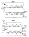
- FIG. 1 shows a schematic diagram of the present invention for a three channel optical transmission line.
- the dispersion compensation node comprises a first optical fibre 1 having an optical circulator input 2 which provides a drop port 3, and a second optical fibre 4 having an optical circulator output 5 which provides a return path to the first optical fibre 1.
- the first optical fibre 1 includes a concatenated series of 2 x 2 non-blocking switches S 1 - S 4 and chirped fibre gratings F 1 - F 3 , each of which is tuned to a respective one of the three possible wavelengths ⁇ 1 - ⁇ 3 .
- the optical circulator input 2 serves as a drop port 3 and the free end of the optical fibre of the first optical fibre 1 is utilised as an insert port 6.
- Suitable switch is the JDS Fitel SR 22 switch.
- Suitable fibre gratings are described by Raman Kashap et al in a paper entitled “A novel method of producing all fibre photo-induced chirped gratings", Electronic Letters, 1994. These gratings, unlike conventional fibre gratings, have a distributed period.
- an example of an optical circulator is the JDS Fitel CR 1500 optical circulator.
- Channels to be reflected are selected by the appropriate switch to the left of the respective grating.
- the final switch S4 ensures that any remaining channels are circulated around the second optical fibre 4 and optical circulator 5 to the input of the chain of fibre gratings.
- the switch positions then ensure that all of the remaining wavelengths are reflected back to the optical circulator output 5 by the previously unused fibre gratings. In this manner, all three channels of the transmission line are reflected from a respective fibre grating and are thus dispersion compensated, and are directed either to the optical output 5 or drop port 3.
- any channels corresponding to those previously dropped from the drop port 3 are directed to the output circulator 5, thus performing an insert function, whilst any channels not previously dropped are reflected straight back to the insert port 6 from the appropriate fibre grating.
- a three channel WDM signal in an optical transmission line is received at the first input circulator 2.
- Channel 1 ( ⁇ 1 ) is reflected from the first grating F 1 in a first optical path whilst channels 2 ( ⁇ 2 ) and 3 ( ⁇ 3 ) pass through unmodified.
- Channel 1 is thus dispersion compensated and directed to the drop port 3 by the optical circulator input 2.
- the switch S 2 is set so that channels 2 and 3 bypass their fibre grating F 2 and F 3 , respectively, circulated around the second optical fibre 4, and are subsequently reflected back to the optical circulator output 5 via switch S 2 by their respective gratings in a second optical path. Accordingly, channels 2 and 3 are dispersion compensated and routed to the node output 5.
- a WDM signal input to the insert port 6 can replace channels which have previously been dropped. For example, with the switch states shown, a signal introduced at the insert port 6 corresponding to channel 1 passes through gratings F 2 and F 3 undisturbed and emerges at the optical circulator output 5. However, channels 2 and 3 will be reflected from their respective gratings and will return to the insert port 6.
- Additional channels may be added simply by inserting an additional 2 x 2 switch and an appropriate chirped fibre grating.
- Figure 3 shows an extension of the dispersion compensation node of Figures 1 and 2 to provide a 2 x 2 cross-point switch.
- the cross-point switch comprises two identical nodes with the drop port fibres 7 and 8 of each dispersion compensation node cross-connected to the first optical fibre 1 of the other i.e. the drop ports 3 and insert ports 6 of the two nodes are cross-connected.
- corresponding switches of the device i.e those with the same switch numbers, are set to the same state to ensure that the same channel is exchanged by the two halves of the cross connect.
- Corresponding chirped fibre gratings are tuned to reflect the same channel ( ⁇ ), but the degree of dispersion compensation provided by each grating may be tuned to take account of the individual transmission line dispersion characteristics.
- FIG. 3 illustrates an example where optical circulators 9 and 10 are provided to achieve this.
- channel 3 on the first compensating node is dropped.
- the drop is set by arranging the first dispersion compensating node to drop channel 1 and 3 and the second dispersion compensating node to drop channel 1.
- the insert port 6 on this node will accept channel 1 from the drop port 3 of the second dispersion compensating node.
- channel 3 has not been dropped from the second dispersion compensating node
- this channel is offered to the insert port 6 of the second dispersion compensating node it is reflected to the local drop port 11 of the optical circulator 9 as shown in the Figure.
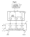
- Figure 5 shows a block diagram of a system for implementing dispersion compensation and drop and insert functions in a two channel transmission line.
- the system comprises a network node controller 12, an XOR logic array 13, and a dispersion compensation node 14 having an optical input 15, an optical output 16, a drop port 17 and an insert port 18.
- the network management controller 12 controls the state of the switches S 1 - S 3 within the dispersion compensating node 14 through the XOR logic array 13. Setting an input to channel 1 ( ⁇ 1 ) or channel 2 ( ⁇ 2 ) to logic "1" in the logic array means that the channel is to be dropped to the drop port 17.
- Channel 0 ( ⁇ 0 ) and channel 3 ( ⁇ 3 ) of the XOR logic array 13 are held at logic "1" and "0", respectively, to implement the required switch settings.
- Figure 6 shows a second example of the present invention where the dispersion compensating node is formed from a single multipoint switch 19 and a number of chirped fibre gratings 20.
- An example of a suitable switch is that sold under the trade name JDS Fitel SG Series MxN Single Mode Matrix Switch.
- the outputs of each fibre grating 20 are connected to the input of the succeeding switching element within the multipoint switch 19.
- the inputs of each of the switching elements are selectively connectable to any of the outputs of the switching elements to perform the required dispersion compensation and any drop and insert function.
- An optical circulator 21 is connected to the input of the first switching element and so provides an optical input 22 and a drop port 23.
- a further optical circulator 24 forms an optical output 25.
- the output of the sixth switching element provides an insert port 26.
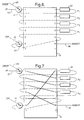
- Figure 7 shows the switch states for an operation which performs dispersion compensation for each of four channels received at the optical input 22 and drops channels 2 and 4.
- the switch states are selected so that the chirped fibre gratings F 2 and F 4 are within a first optical path. Channels 2 and 4 are dispersion compensated in this first optical path and reflected to the drop port 23. The remaining channels pass through these fibre gratings undisturbed and are circulated to a second optical path which includes chirped fibre gratings F 1 and F 3 where channels 1 and 3, respectively, are dispersion compensated and reflected to the optical output 25.
- channels 2 and 4 can be introduced at the insert port 26 from a second transmission line to perform a multiplexing operation. Again, any channels introduced at the insert port 26 which have not been previously dropped will be reflected by their corresponding chirped fibre grating 20 and returned to the insert port 26.
- Figure 8 illustrates the dispersion compensation of all four channels received at the optical input 22 and a drop operation with respect to channel 3.
- Figure 9 shows the dispersion compensation of all four channels received at the optical input 22 and transmission of all four channels to the optical output port 25.
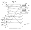
- FIG 10 shows a third example of the present invention which is an extension of the multipoint switch architecture of the second example described with reference to Figures 6 to 10 of the accompanying drawings.
- this third example in addition to the drop port 23 and output port 25, second and third optical circulators 27 and 28, respectively, are provided as drop ports 29 and 30, respectively. This allows the dispersion compensating node to drop channels to more than one other transmission line for routing across an optical network.
- Figure 11 shows the switch states for an operation which performs dispersion compensation for each of four channels received at the optical input 22 and drops channel 2 ( ⁇ 2 ) from drop port 23, drops channel 4 ( ⁇ 4 ) from drop port 29, and transmits channel 1 ( ⁇ 1 ) and channel 3 ( ⁇ 3 ) from the optical output 25.
- insert port 26 is arranged to multiplex channels from other transmission lines (not shown). In this example, drop port 30 is unused.
- the switch states in the dispersion compensating node of Figure 11 are selected so that the chirped fibre grating F 2 is in a first optical path, chirped fibre grating F 4 is in a second optical path, and chirped fibre gratings F 1 and F 3 are in a third optical path.
- Channels tuned to any of the one or more chirped fibre gratings in a particular optical path are reflected by a respective chirped fibre grating to whichever of the optical circulators is coupled via the switching elements to the one or more chirped fibre gratings in that path.
- Channels which are transmitted undisturbed through chirped fibre gratings in an optical path are circulated to the next optical path. In this manner, all of the received channels are circulated within the dispersion compensating node until they reach a corresponding chirped fibre grating and are reflected to the optical output or a drop port, as determined by the switch states.
Landscapes
- Physics & Mathematics (AREA)
- General Physics & Mathematics (AREA)
- Optics & Photonics (AREA)
- Chemical & Material Sciences (AREA)
- Dispersion Chemistry (AREA)
- Electromagnetism (AREA)
- Engineering & Computer Science (AREA)
- Computer Networks & Wireless Communication (AREA)
- Signal Processing (AREA)
- Optical Communication System (AREA)
- Prostheses (AREA)
Description
- "0" = bar
- "1" = cross
| Wavelength | Switch | |||
| 1 (λ1) | 2 (λ2) | S1 | S2 | S3 |
| 0 | 0 | 1 | 0 | 0 |
| 0 | 1 | 1 | 1 | 1 |
| 1 | 0 | 0 | 1 | 0 |
| 1 | 1 | 0 | 0 | 1 |
| Wavelength | Switch | |||||
| 1(λ1) | 2(λ2) | 3(λ3) | S1 | S2 | S3 | S4 |
| 0 | 0 | 0 | 1 | 0 | 0 | 0 |
| 0 | 0 | 1 | 1 | 0 | 1 | 1 |
| 0 | 1 | 0 | 1 | 1 | 1 | 0 |
| 0 | 1 | 1 | 1 | 1 | 0 | 1 |
| 1 | 0 | 0 | 0 | 1 | 0 | 0 |
| 1 | 0 | 1 | 0 | 1 | 1 | 1 |
| 1 | 1 | 0 | 0 | 0 | 1 | 0 |
| 1 | 1 | 1 | 0 | 0 | 0 | 1 |
- Sn=λn-1 XOR λn
- λo= 1 , λN+1=0
Claims (20)
- A chromatic dispersion compensating node for connection to a transmission medium carrying a wavelength division multiplexed optical signal having N channels corresponding to N different wavelengths, comprising:(a) an optical input (2);(b) an optical output (5);(c) at least one drop port (3);(d) a series of N wavelength selective dispersion compensating elements (F1, F2, F3), each of which is tuned to a respective one of N wavelengths, the dispersion compensating elements thereby dispersion compensating all of the N wavelength channels; characterised by(e) switching means (S1, S2, S3, S4) for selectively coupling in a configurable manner each of the N wavelength selective dispersion compensating elements to one of the drop port (3) and the optical output (5), the node thereby selectively dropping one or more of the N channels.
- A dispersion compensating node according to claim 1, comprising a first optical path and a second optical path, wherein the switching means (S1, S2, S3, S4) are arranged selectively to switch a number of the wavelength selective dispersion compensating elements (F1, F2, F3) into the first optical path and selectively switch a number of the remaining wavelength selective dispersion compensating elements (F1, F2, F3) into the second optical path so that signals reflected from dispersion compensating elements in the first optical path are coupled to one of the drop port (3) and the optical output (5), one or more signals transmitted by the dispersion compensating elements (F1, F2, F3) in the first optical path are circulated within the node onto others of the dispersion compensating elements in the second optical path, and signals reflected from dispersion compensating elements (F1, F2, F3) in the second optical path are coupled to the other of the optical output (5) and the drop port (3).
- A dispersion compensating node according to claim 1 or claim 2, comprising a plurality of drop ports (3,11).
- A dispersion compensating node according to any preceding claim, further comprising an insert port (6).
- A dispersion compensating node according to any preceding claim, in which the wavelength selective compensating elements (F1, F2, F3) are chirped fibre gratings.
- A dispersion compensating node according to any preceding claim, in which the optical input (2) and optical output (5) are optical circulators.
- A dispersion compensating node according to any preceding claim, in which the switching means (S1, S2, S3, S4) are a number of discrete 2x2 non-blocking optical switches.
- A dispersion compensating node according to any of claims 1 to 6, in which the switching means comprises an MxN multi-point switch.
- A dispersion compensating node according to any preceding claim, comprising a concatenated series of N wavelength selective dispersion compensating elements (F1, F2, F3) and switching means (S1, S2, S3, S4).
- An optical communication network comprising a number of chromatic dispersion compensating nodes in accordance with any preceding claim.
- An optical communication network according to claim 10, further comprising a network node controller (13) for controlling the switch state of each of the switching elements.
- A cross-point switch for an optical network comprising two chromatic dispersion compensating nodes according to any of claims 1 to 9, in which a drop port (3) of each node is connected to an optical path of the other node.
- A cross-point switch according to claim 12, in which a drop port (3) of one node is connected to an insert port (6) of the other node.
- A cross-point switch according to claim 12 or 13, in which the switch states of the switching means (S1, S2, S3, S4) in the two connected nodes are dependent upon each other.
- A cross-point switch according to claim 12 or 13, in which the switch states of the switching means (S1, S2, S3, S4) are independent of each other.
- A cross-point switch according to claim 15, in which the drop ports (3) include optical circulators to provide a local drop facility.
- An optical communication network comprising a number of cross point switches in accordance with any of claims 12 to 16.
- An optical communication network comprising a combination of one or more chromatic dispersion compensating nodes according to any of claims 1 to 9 and one or more cross point switches according to any of claims 12 to 16.
- A method of dispersion compensating an optical signal having N channels corresponding to N different wavelengths, comprising the steps of:(a) introducing the optical signal to an optical input (2); and(b) communicating the optical signal from the optical input to a series of N wavelength selective dispersion compensating elements (F1, F2, F3) each of which is tuned to a respective one of N wavelengths, the dispersion compensating elements thereby dispersion compensating all of the N wavelength channels; characterised by(c) selectively coupling in a configurable manner each of the N wavelength selective dispersion compensating elements to one of a drop port (3) and an optical output (5), the node thereby selectively dropping one or more of the N channels.
- A method according to claim 19, further comprising the steps of:wherein signals reflected from dispersion compensating elements (F1, F2, F3) in the first optical path are coupled to one of the drop port (3) and the optical output (5), one or more signals transmitted by the dispersion compensating elements (F1, F2, F3) in the first optical path are circulated onto others of the dispersion compensating elements (F1, F2, F3) in the second optical path, and signals reflected from dispersion compensating elements (F1, F2, F3) in the second optical path are coupled to the other of the optical output (5) and the drop port (3).(d) selectively switching a number of the wavelength selective dispersion compensating elements (F1, F2, F3) into a first optical path; and,(e) selectively switching a number of the remaining wavelength selective dispersion compensating elements (F1, F2, F3) into a second optical path,
Priority Applications (1)
| Application Number | Priority Date | Filing Date | Title |
|---|---|---|---|
| EP97906258A EP0890230B1 (en) | 1996-03-29 | 1997-03-05 | Chromatic dispersion compensating node |
Applications Claiming Priority (6)
| Application Number | Priority Date | Filing Date | Title |
|---|---|---|---|
| GBGB9606671.7A GB9606671D0 (en) | 1996-03-29 | 1996-03-29 | Chromatic dispersion compensation |
| GB9606671 | 1996-03-29 | ||
| EP96303452 | 1996-05-15 | ||
| EP96303452 | 1996-05-15 | ||
| EP97906258A EP0890230B1 (en) | 1996-03-29 | 1997-03-05 | Chromatic dispersion compensating node |
| PCT/GB1997/000616 WO1997037446A1 (en) | 1996-03-29 | 1997-03-05 | Chromatic dispersion compensating node |
Publications (2)
| Publication Number | Publication Date |
|---|---|
| EP0890230A1 EP0890230A1 (en) | 1999-01-13 |
| EP0890230B1 true EP0890230B1 (en) | 2001-01-10 |
Family
ID=26143706
Family Applications (1)
| Application Number | Title | Priority Date | Filing Date |
|---|---|---|---|
| EP97906258A Expired - Lifetime EP0890230B1 (en) | 1996-03-29 | 1997-03-05 | Chromatic dispersion compensating node |
Country Status (8)
| Country | Link |
|---|---|
| US (1) | US6122418A (en) |
| EP (1) | EP0890230B1 (en) |
| JP (1) | JP3977430B2 (en) |
| AU (1) | AU728733B2 (en) |
| CA (1) | CA2248081C (en) |
| DE (1) | DE69703880T2 (en) |
| ES (1) | ES2155247T3 (en) |
| WO (1) | WO1997037446A1 (en) |
Families Citing this family (27)
| Publication number | Priority date | Publication date | Assignee | Title |
|---|---|---|---|---|
| IT1283372B1 (en) * | 1996-07-31 | 1998-04-17 | Pirelli Cavi S P A Ora Pirelli | DEVICE FOR THE INSERTION AND EXTRACTION OF OPTICAL SIGNALS |
| JP3492524B2 (en) * | 1998-05-29 | 2004-02-03 | 三菱電機株式会社 | Dispersion compensator |
| US6542275B1 (en) * | 1998-06-29 | 2003-04-01 | Ciena Corporation | Dispersion compensating element having substantially uniform spectral nonlinearity |
| US6304691B1 (en) * | 1998-09-24 | 2001-10-16 | Lucent Technologies,Inc | Wavelength division multiplexed optical communication system having reduced short wavelength loss |
| US6304351B1 (en) * | 1998-10-28 | 2001-10-16 | Tycom (Us) Inc. | Universal branching unit |
| KR100302634B1 (en) * | 1998-12-10 | 2001-11-30 | 서평원 | Modules that monitor and compensate for WDM fiber channel and optical amplifiers |
| JP2000236297A (en) | 1999-02-16 | 2000-08-29 | Fujitsu Ltd | Method and system for optical transmission applied with dispersion compensation |
| US6355886B1 (en) * | 1999-05-21 | 2002-03-12 | Tycom (Us) Inc. | Undersea trunk-and-branch logical ring networks |
| US6295396B1 (en) * | 1999-06-04 | 2001-09-25 | Qtera Corporation | Method and apparatus for higher-order chromatic dispersion compensation |
| GB9915233D0 (en) | 1999-06-30 | 1999-09-01 | Marconi Comm Ltd | Optical system |
| US6317539B1 (en) * | 1999-09-17 | 2001-11-13 | Jds Uniphase Corporation | Interleaved sampled and chirped optical waveguide gratings for WDM channel operations and resulting devices |
| CA2419852A1 (en) * | 2000-08-10 | 2002-02-14 | Siemens Aktiengesellschaft | Optical add drop and dispersion compensation apparatus |
| US7113704B1 (en) * | 2000-11-28 | 2006-09-26 | Kotura, Inc. | Tunable add/drop node for optical network |
| US20040247239A1 (en) * | 2001-03-12 | 2004-12-09 | Louay Eldada | Hitless errorless trimmable dynamic optical add/drop multiplexer devices |
| EP1855132A3 (en) * | 2001-03-12 | 2007-12-26 | E.I.Du pont de nemours and company | Trimmable optical add/drop multiplexer devices |
| GB0108084D0 (en) * | 2001-03-30 | 2001-05-23 | Marconi Comm Ltd | Method and apparatus for providing dispersion in dispersion compensation modules |
| US6944372B2 (en) | 2001-09-21 | 2005-09-13 | Broadband Royalty Corporation | Tunable dispersion compensating bandwidth device for fiber optics system |
| US6738536B2 (en) * | 2001-12-20 | 2004-05-18 | Optinel Systems, Inc. | Wavelength tunable filter device for fiber optic systems |
| US20030219198A1 (en) * | 2002-05-22 | 2003-11-27 | Sycamore Networks, Inc. | Routing in optical networks considering transmission impairments |
| US6810168B1 (en) | 2002-05-30 | 2004-10-26 | Kotura, Inc. | Tunable add/drop node |
| US6931176B2 (en) * | 2002-11-21 | 2005-08-16 | Tropic Networks Inc. | Reconfigurable optical add/drop multiplexer with buried dispersion compensation module |
| US6847763B2 (en) * | 2002-12-17 | 2005-01-25 | Fitel U.S.A. Corp | Colorless tunable dispersion compensator |
| US20050008287A1 (en) * | 2003-07-11 | 2005-01-13 | Red Sky Systems, Inc. | Modular dispersion compensator |
| ES2396784B2 (en) | 2011-03-15 | 2014-07-23 | Medlumics, S.L. | INTEGRABLE ACTIVE EQUALIZATION SYSTEM OF CHROMATIC DISPERSION. |
| US11764872B2 (en) | 2018-09-21 | 2023-09-19 | Telefonaktiebolaget Lm Ericsson (Publ) | Optical dispersion compensator |
| US20230084066A1 (en) * | 2021-09-14 | 2023-03-16 | Huawei Technologies Co., Ltd. | System and method for dispersion compensation in fibered optical communication paths |
| CN113904726B (en) * | 2021-11-15 | 2022-09-16 | 东南大学 | Large time delay difference dispersion waveguide structure |
Family Cites Families (4)
| Publication number | Priority date | Publication date | Assignee | Title |
|---|---|---|---|---|
| US5048909A (en) * | 1990-07-27 | 1991-09-17 | At&T Bell Laboratories | Adiabatic reflection apparatus |
| US5414548A (en) * | 1992-09-29 | 1995-05-09 | Nippon Telegraph And Telephone Corporation | Arrayed-wave guide grating multi/demultiplexer with loop-back optical paths |
| EP0732819A3 (en) * | 1995-03-15 | 1998-03-11 | Sumitomo Electric Industries, Ltd. | Chromatic dispersion compensator and chromatic dispersion compensating optical communication system |
| IT1283405B1 (en) * | 1996-03-11 | 1998-04-21 | Pirelli Cavi S P A Ora Pirelli | METHOD OF SELECTIVE COMPENSATION OF THE CHROMATIC DISPERSION OF OPTICAL SIGNALS |
-
1997
- 1997-03-05 JP JP53499997A patent/JP3977430B2/en not_active Expired - Fee Related
- 1997-03-05 EP EP97906258A patent/EP0890230B1/en not_active Expired - Lifetime
- 1997-03-05 WO PCT/GB1997/000616 patent/WO1997037446A1/en active IP Right Grant
- 1997-03-05 AU AU21003/97A patent/AU728733B2/en not_active Ceased
- 1997-03-05 CA CA002248081A patent/CA2248081C/en not_active Expired - Fee Related
- 1997-03-05 DE DE69703880T patent/DE69703880T2/en not_active Expired - Lifetime
- 1997-03-05 US US09/142,134 patent/US6122418A/en not_active Expired - Lifetime
- 1997-03-05 ES ES97906258T patent/ES2155247T3/en not_active Expired - Lifetime
Also Published As
| Publication number | Publication date |
|---|---|
| ES2155247T3 (en) | 2001-05-01 |
| JP3977430B2 (en) | 2007-09-19 |
| JP2000508138A (en) | 2000-06-27 |
| WO1997037446A1 (en) | 1997-10-09 |
| AU2100397A (en) | 1997-10-22 |
| CA2248081A1 (en) | 1997-10-09 |
| CA2248081C (en) | 2002-12-03 |
| DE69703880T2 (en) | 2001-07-19 |
| US6122418A (en) | 2000-09-19 |
| DE69703880D1 (en) | 2001-02-15 |
| AU728733B2 (en) | 2001-01-18 |
| EP0890230A1 (en) | 1999-01-13 |
Similar Documents
| Publication | Publication Date | Title |
|---|---|---|
| EP0890230B1 (en) | Chromatic dispersion compensating node | |
| US5712932A (en) | Dynamically reconfigurable WDM optical communication systems with optical routing systems | |
| US6115517A (en) | Optical communication network apparatus and optical switching network | |
| EP3410737B1 (en) | Scalable optical switching node | |
| AU626985B2 (en) | Communication network | |
| US6208443B1 (en) | Dynamic optical add-drop multiplexers and wavelength-routing networks with improved survivability and minimized spectral filtering | |
| US7657181B2 (en) | Optical add/drop multiplexer and optical network system | |
| US6519064B1 (en) | Scalable add/drop architecture for lightwave communication system | |
| CA2300886A1 (en) | Wavelength-selective optical switching apparatus, optical communications apparatus using the same, and method for use in the optical communications apparatus | |
| US20030128985A1 (en) | Modular optical network node | |
| CA2332626A1 (en) | Configurable optical add/drop device | |
| US6304351B1 (en) | Universal branching unit | |
| US6859576B2 (en) | Optical cross-connect system | |
| US20020071151A1 (en) | Module and method for reconfiguring optical networks | |
| EP1043847B1 (en) | Wavelength-division multiplex transmission network device using a transceiver having a 2-input/2-output optical switch | |
| EP1407567B1 (en) | Optical filtering by using an add-drop node | |
| JP3444548B2 (en) | Light switch | |
| CA2340148A1 (en) | Optical switch for routing signals and a network incorporating same | |
| EP1017243A2 (en) | Optical switch and optical switched network | |
| AU1498800A (en) | Reconfigurable optical filtering apparatus and a drop-and- insert multiplexer incorporating such apparatus | |
| JP3444543B2 (en) | Optical matrix switch | |
| JP3444544B2 (en) | Optical matrix switch | |
| JPH09224268A (en) | Optical cross connect device | |
| JP2000324052A (en) | Wavelength multiplex type add/drop device and wavelength multiplex type add/drop method |
Legal Events
| Date | Code | Title | Description |
|---|---|---|---|
| PUAI | Public reference made under article 153(3) epc to a published international application that has entered the european phase |
Free format text: ORIGINAL CODE: 0009012 |
|
| 17P | Request for examination filed |
Effective date: 19980831 |
|
| AK | Designated contracting states |
Kind code of ref document: A1 Designated state(s): BE CH DE DK ES FI FR GB IE IT LI NL PT SE |
|
| 17Q | First examination report despatched |
Effective date: 19990406 |
|
| GRAG | Despatch of communication of intention to grant |
Free format text: ORIGINAL CODE: EPIDOS AGRA |
|
| GRAG | Despatch of communication of intention to grant |
Free format text: ORIGINAL CODE: EPIDOS AGRA |
|
| GRAH | Despatch of communication of intention to grant a patent |
Free format text: ORIGINAL CODE: EPIDOS IGRA |
|
| GRAH | Despatch of communication of intention to grant a patent |
Free format text: ORIGINAL CODE: EPIDOS IGRA |
|
| GRAA | (expected) grant |
Free format text: ORIGINAL CODE: 0009210 |
|
| AK | Designated contracting states |
Kind code of ref document: B1 Designated state(s): BE CH DE DK ES FI FR GB IE IT LI NL PT SE |
|
| PG25 | Lapsed in a contracting state [announced via postgrant information from national office to epo] |
Ref country code: SE Free format text: THE PATENT HAS BEEN ANNULLED BY A DECISION OF A NATIONAL AUTHORITY Effective date: 20010110 Ref country code: NL Free format text: LAPSE BECAUSE OF FAILURE TO SUBMIT A TRANSLATION OF THE DESCRIPTION OR TO PAY THE FEE WITHIN THE PRESCRIBED TIME-LIMIT Effective date: 20010110 Ref country code: FI Free format text: LAPSE BECAUSE OF FAILURE TO SUBMIT A TRANSLATION OF THE DESCRIPTION OR TO PAY THE FEE WITHIN THE PRESCRIBED TIME-LIMIT Effective date: 20010110 |
|
| REG | Reference to a national code |
Ref country code: CH Ref legal event code: EP |
|
| REG | Reference to a national code |
Ref country code: IE Ref legal event code: FG4D |
|
| REF | Corresponds to: |
Ref document number: 69703880 Country of ref document: DE Date of ref document: 20010215 |
|
| PG25 | Lapsed in a contracting state [announced via postgrant information from national office to epo] |
Ref country code: IE Free format text: LAPSE BECAUSE OF NON-PAYMENT OF DUE FEES Effective date: 20010305 |
|
| ITF | It: translation for a ep patent filed | ||
| PG25 | Lapsed in a contracting state [announced via postgrant information from national office to epo] |
Ref country code: PT Free format text: LAPSE BECAUSE OF FAILURE TO SUBMIT A TRANSLATION OF THE DESCRIPTION OR TO PAY THE FEE WITHIN THE PRESCRIBED TIME-LIMIT Effective date: 20010410 Ref country code: DK Free format text: LAPSE BECAUSE OF FAILURE TO SUBMIT A TRANSLATION OF THE DESCRIPTION OR TO PAY THE FEE WITHIN THE PRESCRIBED TIME-LIMIT Effective date: 20010410 |
|
| REG | Reference to a national code |
Ref country code: CH Ref legal event code: NV Representative=s name: JACOBACCI & PERANI S.A. |
|
| REG | Reference to a national code |
Ref country code: ES Ref legal event code: FG2A Ref document number: 2155247 Country of ref document: ES Kind code of ref document: T3 |
|
| ET | Fr: translation filed | ||
| NLV1 | Nl: lapsed or annulled due to failure to fulfill the requirements of art. 29p and 29m of the patents act | ||
| PLBE | No opposition filed within time limit |
Free format text: ORIGINAL CODE: 0009261 |
|
| STAA | Information on the status of an ep patent application or granted ep patent |
Free format text: STATUS: NO OPPOSITION FILED WITHIN TIME LIMIT |
|
| REG | Reference to a national code |
Ref country code: GB Ref legal event code: IF02 |
|
| 26N | No opposition filed | ||
| REG | Reference to a national code |
Ref country code: IE Ref legal event code: MM4A |
|
| PGFP | Annual fee paid to national office [announced via postgrant information from national office to epo] |
Ref country code: CH Payment date: 20020214 Year of fee payment: 6 |
|
| PGFP | Annual fee paid to national office [announced via postgrant information from national office to epo] |
Ref country code: ES Payment date: 20020308 Year of fee payment: 6 Ref country code: BE Payment date: 20020308 Year of fee payment: 6 |
|
| REG | Reference to a national code |
Ref country code: GB Ref legal event code: 732E |
|
| PG25 | Lapsed in a contracting state [announced via postgrant information from national office to epo] |
Ref country code: ES Free format text: LAPSE BECAUSE OF NON-PAYMENT OF DUE FEES Effective date: 20030306 |
|
| PG25 | Lapsed in a contracting state [announced via postgrant information from national office to epo] |
Ref country code: LI Free format text: LAPSE BECAUSE OF NON-PAYMENT OF DUE FEES Effective date: 20030331 Ref country code: CH Free format text: LAPSE BECAUSE OF NON-PAYMENT OF DUE FEES Effective date: 20030331 Ref country code: BE Free format text: LAPSE BECAUSE OF NON-PAYMENT OF DUE FEES Effective date: 20030331 |
|
| BERE | Be: lapsed |
Owner name: BRITISH *TELECOMMUNICATIONS P.L.C. Effective date: 20030331 |
|
| REG | Reference to a national code |
Ref country code: CH Ref legal event code: PL |
|
| REG | Reference to a national code |
Ref country code: ES Ref legal event code: FD2A Effective date: 20030306 |
|
| PG25 | Lapsed in a contracting state [announced via postgrant information from national office to epo] |
Ref country code: IT Free format text: LAPSE BECAUSE OF NON-PAYMENT OF DUE FEES Effective date: 20050305 |
|
| REG | Reference to a national code |
Ref country code: FR Ref legal event code: PLFP Year of fee payment: 19 |
|
| PGFP | Annual fee paid to national office [announced via postgrant information from national office to epo] |
Ref country code: DE Payment date: 20150320 Year of fee payment: 19 |
|
| PGFP | Annual fee paid to national office [announced via postgrant information from national office to epo] |
Ref country code: GB Payment date: 20150319 Year of fee payment: 19 Ref country code: FR Payment date: 20150319 Year of fee payment: 19 |
|
| REG | Reference to a national code |
Ref country code: DE Ref legal event code: R119 Ref document number: 69703880 Country of ref document: DE |
|
| GBPC | Gb: european patent ceased through non-payment of renewal fee |
Effective date: 20160305 |
|
| REG | Reference to a national code |
Ref country code: FR Ref legal event code: ST Effective date: 20161130 |
|
| PG25 | Lapsed in a contracting state [announced via postgrant information from national office to epo] |
Ref country code: DE Free format text: LAPSE BECAUSE OF NON-PAYMENT OF DUE FEES Effective date: 20161001 Ref country code: FR Free format text: LAPSE BECAUSE OF NON-PAYMENT OF DUE FEES Effective date: 20160331 Ref country code: GB Free format text: LAPSE BECAUSE OF NON-PAYMENT OF DUE FEES Effective date: 20160305 |