EP0889350A1 - Photoluminescent display devices (I) - Google Patents
Photoluminescent display devices (I) Download PDFInfo
- Publication number
- EP0889350A1 EP0889350A1 EP97111229A EP97111229A EP0889350A1 EP 0889350 A1 EP0889350 A1 EP 0889350A1 EP 97111229 A EP97111229 A EP 97111229A EP 97111229 A EP97111229 A EP 97111229A EP 0889350 A1 EP0889350 A1 EP 0889350A1
- Authority
- EP
- European Patent Office
- Prior art keywords
- polarized
- display device
- layer
- light
- thin
- Prior art date
- Legal status (The legal status is an assumption and is not a legal conclusion. Google has not performed a legal analysis and makes no representation as to the accuracy of the status listed.)
- Withdrawn
Links
- 238000010521 absorption reaction Methods 0.000 claims abstract description 46
- 230000010287 polarization Effects 0.000 claims abstract description 32
- 239000004973 liquid crystal related substance Substances 0.000 claims description 26
- 239000000463 material Substances 0.000 claims description 20
- 229920000642 polymer Polymers 0.000 claims description 19
- 238000000034 method Methods 0.000 claims description 12
- 238000000862 absorption spectrum Methods 0.000 claims description 7
- 238000000295 emission spectrum Methods 0.000 claims description 6
- 239000000126 substance Substances 0.000 claims description 6
- 210000002858 crystal cell Anatomy 0.000 claims description 3
- 230000005693 optoelectronics Effects 0.000 claims description 2
- 238000003491 array Methods 0.000 claims 1
- 238000005424 photoluminescence Methods 0.000 description 147
- 230000009102 absorption Effects 0.000 description 42
- 210000004027 cell Anatomy 0.000 description 31
- 239000003086 colorant Substances 0.000 description 19
- 239000004698 Polyethylene Substances 0.000 description 18
- 239000000203 mixture Substances 0.000 description 18
- 230000005284 excitation Effects 0.000 description 17
- 230000000694 effects Effects 0.000 description 16
- 229920000785 ultra high molecular weight polyethylene Polymers 0.000 description 14
- 230000008859 change Effects 0.000 description 13
- 230000008901 benefit Effects 0.000 description 10
- 238000004519 manufacturing process Methods 0.000 description 9
- 229920000109 alkoxy-substituted poly(p-phenylene vinylene) Polymers 0.000 description 8
- 239000000975 dye Substances 0.000 description 8
- 239000007788 liquid Substances 0.000 description 8
- 230000003287 optical effect Effects 0.000 description 8
- 229920002959 polymer blend Polymers 0.000 description 8
- 239000002178 crystalline material Substances 0.000 description 7
- 230000005684 electric field Effects 0.000 description 7
- 230000006870 function Effects 0.000 description 7
- 230000005540 biological transmission Effects 0.000 description 5
- 239000007850 fluorescent dye Substances 0.000 description 5
- 230000000052 comparative effect Effects 0.000 description 4
- 229920002495 polyphenylene ethynylene polymer Polymers 0.000 description 4
- 238000002360 preparation method Methods 0.000 description 4
- 241000894007 species Species 0.000 description 4
- 238000001228 spectrum Methods 0.000 description 4
- 238000005266 casting Methods 0.000 description 3
- 239000003795 chemical substances by application Substances 0.000 description 3
- 230000006872 improvement Effects 0.000 description 3
- 239000011159 matrix material Substances 0.000 description 3
- 239000000243 solution Substances 0.000 description 3
- CTQNGGLPUBDAKN-UHFFFAOYSA-N O-Xylene Chemical compound CC1=CC=CC=C1C CTQNGGLPUBDAKN-UHFFFAOYSA-N 0.000 description 2
- 239000004699 Ultra-high molecular weight polyethylene Substances 0.000 description 2
- 125000003545 alkoxy group Chemical group 0.000 description 2
- 230000009286 beneficial effect Effects 0.000 description 2
- 230000008033 biological extinction Effects 0.000 description 2
- 238000007872 degassing Methods 0.000 description 2
- 238000004090 dissolution Methods 0.000 description 2
- 239000002019 doping agent Substances 0.000 description 2
- 239000000499 gel Substances 0.000 description 2
- 229910010272 inorganic material Inorganic materials 0.000 description 2
- 239000011147 inorganic material Substances 0.000 description 2
- 229920002521 macromolecule Polymers 0.000 description 2
- 239000011368 organic material Substances 0.000 description 2
- 230000001443 photoexcitation Effects 0.000 description 2
- 238000000103 photoluminescence spectrum Methods 0.000 description 2
- -1 poly(tetrafluoroethylene) Polymers 0.000 description 2
- 238000007639 printing Methods 0.000 description 2
- 239000007787 solid Substances 0.000 description 2
- 239000008096 xylene Substances 0.000 description 2
- IIZPXYDJLKNOIY-JXPKJXOSSA-N 1-palmitoyl-2-arachidonoyl-sn-glycero-3-phosphocholine Chemical compound CCCCCCCCCCCCCCCC(=O)OC[C@H](COP([O-])(=O)OCC[N+](C)(C)C)OC(=O)CCC\C=C/C\C=C/C\C=C/C\C=C/CCCCC IIZPXYDJLKNOIY-JXPKJXOSSA-N 0.000 description 1
- ROFVEXUMMXZLPA-UHFFFAOYSA-N Bipyridyl Chemical compound N1=CC=CC=C1C1=CC=CC=N1 ROFVEXUMMXZLPA-UHFFFAOYSA-N 0.000 description 1
- 239000004986 Cholesteric liquid crystals (ChLC) Substances 0.000 description 1
- VYZAMTAEIAYCRO-UHFFFAOYSA-N Chromium Chemical compound [Cr] VYZAMTAEIAYCRO-UHFFFAOYSA-N 0.000 description 1
- 239000004705 High-molecular-weight polyethylene Substances 0.000 description 1
- 238000001074 Langmuir--Blodgett assembly Methods 0.000 description 1
- OAICVXFJPJFONN-UHFFFAOYSA-N Phosphorus Chemical compound [P] OAICVXFJPJFONN-UHFFFAOYSA-N 0.000 description 1
- 239000004642 Polyimide Substances 0.000 description 1
- XUIMIQQOPSSXEZ-UHFFFAOYSA-N Silicon Chemical compound [Si] XUIMIQQOPSSXEZ-UHFFFAOYSA-N 0.000 description 1
- 239000007983 Tris buffer Substances 0.000 description 1
- 238000004847 absorption spectroscopy Methods 0.000 description 1
- 229910052782 aluminium Inorganic materials 0.000 description 1
- XAGFODPZIPBFFR-UHFFFAOYSA-N aluminium Chemical compound [Al] XAGFODPZIPBFFR-UHFFFAOYSA-N 0.000 description 1
- 239000004411 aluminium Substances 0.000 description 1
- 238000004458 analytical method Methods 0.000 description 1
- 238000000149 argon plasma sintering Methods 0.000 description 1
- 125000000732 arylene group Chemical group 0.000 description 1
- 238000012512 characterization method Methods 0.000 description 1
- 229910052804 chromium Inorganic materials 0.000 description 1
- 239000011651 chromium Substances 0.000 description 1
- 239000011248 coating agent Substances 0.000 description 1
- 238000000576 coating method Methods 0.000 description 1
- 239000000084 colloidal system Substances 0.000 description 1
- 239000012141 concentrate Substances 0.000 description 1
- 239000002322 conducting polymer Substances 0.000 description 1
- 229920001940 conductive polymer Polymers 0.000 description 1
- 230000001419 dependent effect Effects 0.000 description 1
- 238000000151 deposition Methods 0.000 description 1
- 230000008021 deposition Effects 0.000 description 1
- 238000013461 design Methods 0.000 description 1
- 239000006185 dispersion Substances 0.000 description 1
- 238000006073 displacement reaction Methods 0.000 description 1
- 239000007772 electrode material Substances 0.000 description 1
- 238000005516 engineering process Methods 0.000 description 1
- 230000007613 environmental effect Effects 0.000 description 1
- 238000001704 evaporation Methods 0.000 description 1
- 230000008020 evaporation Effects 0.000 description 1
- 238000001914 filtration Methods 0.000 description 1
- 239000012530 fluid Substances 0.000 description 1
- 238000005286 illumination Methods 0.000 description 1
- 238000010348 incorporation Methods 0.000 description 1
- AMGQUBHHOARCQH-UHFFFAOYSA-N indium;oxotin Chemical compound [In].[Sn]=O AMGQUBHHOARCQH-UHFFFAOYSA-N 0.000 description 1
- 229940067606 lecithin Drugs 0.000 description 1
- 235000010445 lecithin Nutrition 0.000 description 1
- 239000000787 lecithin Substances 0.000 description 1
- 230000031700 light absorption Effects 0.000 description 1
- 238000005259 measurement Methods 0.000 description 1
- 238000002156 mixing Methods 0.000 description 1
- 230000007935 neutral effect Effects 0.000 description 1
- 239000003921 oil Substances 0.000 description 1
- 230000008520 organization Effects 0.000 description 1
- 239000002245 particle Substances 0.000 description 1
- 229920001721 polyimide Polymers 0.000 description 1
- 229920001343 polytetrafluoroethylene Polymers 0.000 description 1
- 239000010453 quartz Substances 0.000 description 1
- 230000005855 radiation Effects 0.000 description 1
- 230000010076 replication Effects 0.000 description 1
- YAYGSLOSTXKUBW-UHFFFAOYSA-N ruthenium(2+) Chemical compound [Ru+2] YAYGSLOSTXKUBW-UHFFFAOYSA-N 0.000 description 1
- SBIBMFFZSBJNJF-UHFFFAOYSA-N selenium;zinc Chemical compound [Se]=[Zn] SBIBMFFZSBJNJF-UHFFFAOYSA-N 0.000 description 1
- 229910052710 silicon Inorganic materials 0.000 description 1
- 239000010703 silicon Substances 0.000 description 1
- VYPSYNLAJGMNEJ-UHFFFAOYSA-N silicon dioxide Inorganic materials O=[Si]=O VYPSYNLAJGMNEJ-UHFFFAOYSA-N 0.000 description 1
- 150000003384 small molecules Chemical class 0.000 description 1
- 125000006850 spacer group Chemical group 0.000 description 1
- 238000004544 sputter deposition Methods 0.000 description 1
- 239000000758 substrate Substances 0.000 description 1
- 239000004094 surface-active agent Substances 0.000 description 1
- 229920002994 synthetic fiber Polymers 0.000 description 1
- 238000012546 transfer Methods 0.000 description 1
- 230000007704 transition Effects 0.000 description 1
- 238000002834 transmittance Methods 0.000 description 1
- 239000012780 transparent material Substances 0.000 description 1
- 230000016776 visual perception Effects 0.000 description 1
- 239000011800 void material Substances 0.000 description 1
Images
Classifications
-
- G—PHYSICS
- G02—OPTICS
- G02F—OPTICAL DEVICES OR ARRANGEMENTS FOR THE CONTROL OF LIGHT BY MODIFICATION OF THE OPTICAL PROPERTIES OF THE MEDIA OF THE ELEMENTS INVOLVED THEREIN; NON-LINEAR OPTICS; FREQUENCY-CHANGING OF LIGHT; OPTICAL LOGIC ELEMENTS; OPTICAL ANALOGUE/DIGITAL CONVERTERS
- G02F1/00—Devices or arrangements for the control of the intensity, colour, phase, polarisation or direction of light arriving from an independent light source, e.g. switching, gating or modulating; Non-linear optics
- G02F1/01—Devices or arrangements for the control of the intensity, colour, phase, polarisation or direction of light arriving from an independent light source, e.g. switching, gating or modulating; Non-linear optics for the control of the intensity, phase, polarisation or colour
- G02F1/13—Devices or arrangements for the control of the intensity, colour, phase, polarisation or direction of light arriving from an independent light source, e.g. switching, gating or modulating; Non-linear optics for the control of the intensity, phase, polarisation or colour based on liquid crystals, e.g. single liquid crystal display cells
- G02F1/133—Constructional arrangements; Operation of liquid crystal cells; Circuit arrangements
- G02F1/1333—Constructional arrangements; Manufacturing methods
- G02F1/1335—Structural association of cells with optical devices, e.g. polarisers or reflectors
- G02F1/1336—Illuminating devices
- G02F1/133617—Illumination with ultraviolet light; Luminescent elements or materials associated to the cell
-
- G—PHYSICS
- G02—OPTICS
- G02F—OPTICAL DEVICES OR ARRANGEMENTS FOR THE CONTROL OF LIGHT BY MODIFICATION OF THE OPTICAL PROPERTIES OF THE MEDIA OF THE ELEMENTS INVOLVED THEREIN; NON-LINEAR OPTICS; FREQUENCY-CHANGING OF LIGHT; OPTICAL LOGIC ELEMENTS; OPTICAL ANALOGUE/DIGITAL CONVERTERS
- G02F1/00—Devices or arrangements for the control of the intensity, colour, phase, polarisation or direction of light arriving from an independent light source, e.g. switching, gating or modulating; Non-linear optics
- G02F1/01—Devices or arrangements for the control of the intensity, colour, phase, polarisation or direction of light arriving from an independent light source, e.g. switching, gating or modulating; Non-linear optics for the control of the intensity, phase, polarisation or colour
- G02F1/13—Devices or arrangements for the control of the intensity, colour, phase, polarisation or direction of light arriving from an independent light source, e.g. switching, gating or modulating; Non-linear optics for the control of the intensity, phase, polarisation or colour based on liquid crystals, e.g. single liquid crystal display cells
- G02F1/133—Constructional arrangements; Operation of liquid crystal cells; Circuit arrangements
- G02F1/1333—Constructional arrangements; Manufacturing methods
- G02F1/1335—Structural association of cells with optical devices, e.g. polarisers or reflectors
- G02F1/133528—Polarisers
-
- G—PHYSICS
- G02—OPTICS
- G02F—OPTICAL DEVICES OR ARRANGEMENTS FOR THE CONTROL OF LIGHT BY MODIFICATION OF THE OPTICAL PROPERTIES OF THE MEDIA OF THE ELEMENTS INVOLVED THEREIN; NON-LINEAR OPTICS; FREQUENCY-CHANGING OF LIGHT; OPTICAL LOGIC ELEMENTS; OPTICAL ANALOGUE/DIGITAL CONVERTERS
- G02F1/00—Devices or arrangements for the control of the intensity, colour, phase, polarisation or direction of light arriving from an independent light source, e.g. switching, gating or modulating; Non-linear optics
- G02F1/01—Devices or arrangements for the control of the intensity, colour, phase, polarisation or direction of light arriving from an independent light source, e.g. switching, gating or modulating; Non-linear optics for the control of the intensity, phase, polarisation or colour
- G02F1/13—Devices or arrangements for the control of the intensity, colour, phase, polarisation or direction of light arriving from an independent light source, e.g. switching, gating or modulating; Non-linear optics for the control of the intensity, phase, polarisation or colour based on liquid crystals, e.g. single liquid crystal display cells
- G02F1/133—Constructional arrangements; Operation of liquid crystal cells; Circuit arrangements
- G02F1/1333—Constructional arrangements; Manufacturing methods
- G02F1/1347—Arrangement of liquid crystal layers or cells in which the final condition of one light beam is achieved by the addition of the effects of two or more layers or cells
- G02F1/13471—Arrangement of liquid crystal layers or cells in which the final condition of one light beam is achieved by the addition of the effects of two or more layers or cells in which all the liquid crystal cells or layers remain transparent, e.g. FLC, ECB, DAP, HAN, TN, STN, SBE-LC cells
- G02F1/13473—Arrangement of liquid crystal layers or cells in which the final condition of one light beam is achieved by the addition of the effects of two or more layers or cells in which all the liquid crystal cells or layers remain transparent, e.g. FLC, ECB, DAP, HAN, TN, STN, SBE-LC cells for wavelength filtering or for colour display without the use of colour mosaic filters
-
- G—PHYSICS
- G02—OPTICS
- G02F—OPTICAL DEVICES OR ARRANGEMENTS FOR THE CONTROL OF LIGHT BY MODIFICATION OF THE OPTICAL PROPERTIES OF THE MEDIA OF THE ELEMENTS INVOLVED THEREIN; NON-LINEAR OPTICS; FREQUENCY-CHANGING OF LIGHT; OPTICAL LOGIC ELEMENTS; OPTICAL ANALOGUE/DIGITAL CONVERTERS
- G02F1/00—Devices or arrangements for the control of the intensity, colour, phase, polarisation or direction of light arriving from an independent light source, e.g. switching, gating or modulating; Non-linear optics
- G02F1/01—Devices or arrangements for the control of the intensity, colour, phase, polarisation or direction of light arriving from an independent light source, e.g. switching, gating or modulating; Non-linear optics for the control of the intensity, phase, polarisation or colour
- G02F1/13—Devices or arrangements for the control of the intensity, colour, phase, polarisation or direction of light arriving from an independent light source, e.g. switching, gating or modulating; Non-linear optics for the control of the intensity, phase, polarisation or colour based on liquid crystals, e.g. single liquid crystal display cells
- G02F1/133—Constructional arrangements; Operation of liquid crystal cells; Circuit arrangements
- G02F1/1333—Constructional arrangements; Manufacturing methods
- G02F1/1335—Structural association of cells with optical devices, e.g. polarisers or reflectors
- G02F1/133528—Polarisers
- G02F1/133533—Colour selective polarisers
-
- G—PHYSICS
- G02—OPTICS
- G02F—OPTICAL DEVICES OR ARRANGEMENTS FOR THE CONTROL OF LIGHT BY MODIFICATION OF THE OPTICAL PROPERTIES OF THE MEDIA OF THE ELEMENTS INVOLVED THEREIN; NON-LINEAR OPTICS; FREQUENCY-CHANGING OF LIGHT; OPTICAL LOGIC ELEMENTS; OPTICAL ANALOGUE/DIGITAL CONVERTERS
- G02F1/00—Devices or arrangements for the control of the intensity, colour, phase, polarisation or direction of light arriving from an independent light source, e.g. switching, gating or modulating; Non-linear optics
- G02F1/01—Devices or arrangements for the control of the intensity, colour, phase, polarisation or direction of light arriving from an independent light source, e.g. switching, gating or modulating; Non-linear optics for the control of the intensity, phase, polarisation or colour
- G02F1/13—Devices or arrangements for the control of the intensity, colour, phase, polarisation or direction of light arriving from an independent light source, e.g. switching, gating or modulating; Non-linear optics for the control of the intensity, phase, polarisation or colour based on liquid crystals, e.g. single liquid crystal display cells
- G02F1/133—Constructional arrangements; Operation of liquid crystal cells; Circuit arrangements
- G02F1/1333—Constructional arrangements; Manufacturing methods
- G02F1/1335—Structural association of cells with optical devices, e.g. polarisers or reflectors
- G02F1/1336—Illuminating devices
- G02F1/133614—Illuminating devices using photoluminescence, e.g. phosphors illuminated by UV or blue light
-
- G—PHYSICS
- G02—OPTICS
- G02F—OPTICAL DEVICES OR ARRANGEMENTS FOR THE CONTROL OF LIGHT BY MODIFICATION OF THE OPTICAL PROPERTIES OF THE MEDIA OF THE ELEMENTS INVOLVED THEREIN; NON-LINEAR OPTICS; FREQUENCY-CHANGING OF LIGHT; OPTICAL LOGIC ELEMENTS; OPTICAL ANALOGUE/DIGITAL CONVERTERS
- G02F1/00—Devices or arrangements for the control of the intensity, colour, phase, polarisation or direction of light arriving from an independent light source, e.g. switching, gating or modulating; Non-linear optics
- G02F1/01—Devices or arrangements for the control of the intensity, colour, phase, polarisation or direction of light arriving from an independent light source, e.g. switching, gating or modulating; Non-linear optics for the control of the intensity, phase, polarisation or colour
- G02F1/13—Devices or arrangements for the control of the intensity, colour, phase, polarisation or direction of light arriving from an independent light source, e.g. switching, gating or modulating; Non-linear optics for the control of the intensity, phase, polarisation or colour based on liquid crystals, e.g. single liquid crystal display cells
- G02F1/133—Constructional arrangements; Operation of liquid crystal cells; Circuit arrangements
- G02F1/1333—Constructional arrangements; Manufacturing methods
- G02F1/1335—Structural association of cells with optical devices, e.g. polarisers or reflectors
- G02F1/1336—Illuminating devices
- G02F1/13362—Illuminating devices providing polarized light, e.g. by converting a polarisation component into another one
-
- G—PHYSICS
- G02—OPTICS
- G02F—OPTICAL DEVICES OR ARRANGEMENTS FOR THE CONTROL OF LIGHT BY MODIFICATION OF THE OPTICAL PROPERTIES OF THE MEDIA OF THE ELEMENTS INVOLVED THEREIN; NON-LINEAR OPTICS; FREQUENCY-CHANGING OF LIGHT; OPTICAL LOGIC ELEMENTS; OPTICAL ANALOGUE/DIGITAL CONVERTERS
- G02F1/00—Devices or arrangements for the control of the intensity, colour, phase, polarisation or direction of light arriving from an independent light source, e.g. switching, gating or modulating; Non-linear optics
- G02F1/01—Devices or arrangements for the control of the intensity, colour, phase, polarisation or direction of light arriving from an independent light source, e.g. switching, gating or modulating; Non-linear optics for the control of the intensity, phase, polarisation or colour
- G02F1/13—Devices or arrangements for the control of the intensity, colour, phase, polarisation or direction of light arriving from an independent light source, e.g. switching, gating or modulating; Non-linear optics for the control of the intensity, phase, polarisation or colour based on liquid crystals, e.g. single liquid crystal display cells
- G02F1/133—Constructional arrangements; Operation of liquid crystal cells; Circuit arrangements
- G02F1/1333—Constructional arrangements; Manufacturing methods
- G02F1/1337—Surface-induced orientation of the liquid crystal molecules, e.g. by alignment layers
- G02F1/133711—Surface-induced orientation of the liquid crystal molecules, e.g. by alignment layers by organic films, e.g. polymeric films
Definitions
- the present invention relates to display devices and in particular to displays comprising at least one photoluminescent layer that is characterized in a high degree of polarization in its absorption.
- Optoelectronic display devices such as those based on the Electrically Controlled Birefringence (ECB) effect, the Twisted Nematic (TN) effect and Super-Twisted Nematic (STN) effect (S. W. Depp et al., Sci. Am., Vol. 268, p. 40 (1993); T. Scheffer et al., in "Liquid Crystals, Applications and Uses", Vol. 1, B. Bahadur, Ed., Chapter 10, pp. 231-274 (1990), Worlds Scientific, Singapore; S. Morozumi, ibid., Chapter 7, pp. 171-194), are well known in the art and are of major importance in a large variety of applications.
- EBCB Electrically Controlled Birefringence
- TN Twisted Nematic
- STN Super-Twisted Nematic
- a liquid crystalline material is sandwiched in a cell ( 3 ) between two light-polarizing means ( 4 ) and the liquid crystalline material is used to electrically rotate the polarization direction of polarized light and, thus, the structure functions as a light valve.
- Polarized light is produced in these devices by a first polarizer, and a second polarizer (also referred to as analyzer) is used to generate visual perception of the electrical switching of the liquid crystalline material.
- a thin layer of well-ordered liquid crystalline material has the ability to change the state of polarization of light that passes through it.
- the LC order can be controlled by means of an electrical field, electric switching can modulate the polarization of the transmitted light.
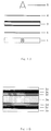
- a cell structure cf. Figs. 1 A, B
- spacered transparent carrier plates 3b
- two transparent electrodes 3c
- the transparent electrode material can be, for instance, indium tin oxide, but may also consist of a transparent conducting polymer.
- the molecular organization within the liquid crystal layer is planar and well-controlled by orientation layers ( 3d ) applied on the electrodes and/or by the presence of small amounts of chiral dopants in the liquid crystal mixture.
- the LC material is aligned perfectly perpendicular to the electrode surfaces and behaves isotropically for the light which passes parallel to the field lines. This means that the state of polarization of light that passes the cell remains unaffected.
- intermediate voltages also intermediate states of orientation can be achieved in which the director, being the local direction of the average orientation of the LC molecules, describes a complicated pattern over the thickness of the cell, which can be used to create intermediate scales between the fully-off and the fully-on state.
- a common dichroic sheet polarizer usually absorbs at least 50 % of the incident light. In a typical TN display, more than 80 % of the incident light is absorbed by the polarizers and color filters and, consequently, the brightness of the displays is very limited. The poor light efficiency of these displays, generally, is compensated by rather intense backlighting which limits the life-time of batteries in devices such as lap-top computers and portable telephones. Moreover, conventional polarizers transfer the absorbed light into heat and, consequently, exhibit excessive heating-up when used in combination with high-intensity light sources. These high-intensity light sources are employed in applications such as projection televisions, and the polarizers limit the life-time of the displays in these applications.
- a display device that comprises an at least partially mirrored polymer plate (cf. Fig. 2, ( A )) in which a fluorescent dye is dissolved and that further comprises a means ( B ) positioned behind the polymer plate ( A ), from the light-exit direction, that allows transmission of only that part of the light spectrum that is absorbed by the fluorescent plate ( A ).
- a plate ( A ) can be used in which form-anisotropic fluorescent molecules are dissolved in a uniform orientation within the polymer plate.
- the proposed display configurations suffer a number of drawbacks, most of which are directly related to the dimensions of the plate.
- the light collection area of the fluorescent plate must be substantially larger than the area of the electrooptical light valve to provide enough of the necessary radiation.
- These displays are therefore only suitable for applications where there is enough room for such a plate such as measuring instruments or digital clocks (M. Bechter et. al., Electronics, December 8, pp. 113-116 (1977)).
- G. Baur et al. Appl. Phys. Lett., Vol. 31, pp. 4-6 (1977); W. Greubel et. al., Elektronik, pp.
- the fluorescent plate needs to be thick (> 1 mm) to generate a high absorption of environmental light.
- the dye concentration in the plate must be low to avoid "self-absorption” and consequently the plate thickness must be high to generate a light absorption close to 100 %.
- the plates act as waveguides for the fluorescent light and the light travels distances between 1 to 100 cm in the plate before it is coupled out. Consequently, the light output (brightness) is strongly reduced by the overlap of the absorption and emission spectrum of the fluorescent dyes.
- plates have to be produced from highly transparent materials with perfect optical surfaces and perfectly reflecting layers at the narrow sides are required.
- One object of the present invention to overcome the problems of the prior art displays. Is to provide a display device that comprises at least one thin, photoluminescent layer that is characterized in a high degree of polarization in its absorption and that is characterized by an emission which Is either polarized or not polarized.
- Another object of the present invention it to provide a display device that comprises one photoluminescent layer that is characterized in a high degree of polarization in its absorption, and one polarizer or analyzer.
- Yet another object of the present invention it to provide a display device that comprises a first photoluminescent layer that is characterized in a high degree of polarization in Its absorption, and a second photoluminescent layer that is characterized in a high degree of polarization in its absorption, and that is further characterized in that the two layers have different photoemission or absorption spectra or both.
- Still another object of the present invention is to provide a display device that comprises multiple photoluminescent layers that are characterized in a high degree of polarization in their absorption, and multiple electrooptic light valves, arranged in a stacked fashion, and that is further characterized in that the layers different photoemission or absorption spectra or both.
- Another object of the present invention is to provide a display device that comprises at least one thin, photoluminescent layer that is characterized in a high degree of polarization in its absorption and that is characterized by an emission which is either polarized or not polarized and that is characterized by small dimensions in the thickness direction and area.
- the present invention is based on our surprising finding that display devices comprising at least one thin photoluminescent layer that is characterized in a high degree of polarization in its absorption are of a very high brightness and very high contrast, have an excellent viewing angle, and can be configured to exhibit one or more colors that cover the entire visible portion of the spectrum of light useful for display applications.
- the designation photoluminescent and photoluminescence are abbreviated with the designation PL
- the term polarized PL layer refers to a photoluminescent layer that is characterized in a high degree of polarization in its absorption and that is characterized in an emission which is either polarized or not polarized.
- the polarized PL layers should be thin and should exhibit a dichroic ratio that exceeds a minimum value in order to yield displays with the above desired characteristics.
- device elements such as layer, electrooptical light valve, polarizer, light source, and mirror are sometimes referred to in their singular form, which should not be construed as to imply that reference is made to only one such element.
- the dichroic ratio in absorption is defined as the ratio of the highest possible absorption of linear polarized light to the lowest possible absorption of linear polarised light. These absorptions are measured at the same single wavelength somewhere within the absorption spectrum and preferentially at an absorption maximum.
- the dichroic ratio in emission is defined as the highest possible emission of linear polarized light to the lowest possible emission of linear polarized light. These emissions are measured at the same single wavelength using unpolarized excitation light at a single wavelength somewhere within the emission spectrum and preferentially at an emission maximum.
- the present invention is based on our surprising finding that display devices comprising at least one thin highly polarized PL layer are of a very high brightness and very high contrast, have an excellent viewing angle, and can be configured to exhibit one or more colors that cover the entire visible portion of the spectrum of light useful for display applications. Most importantly, we found that the polarized PL layers should be thin and should exhibit a dichroic ratio in absorption that exceeds a minimum value in order to yield displays with the above desired characteristics.
- the polarized PL layers useful in the present invention are characterized in that they absorb light in a highly polarized fashion and, after photoexcitation, they emit light that can be polarized or not.
- Such polarized PL layers can comprise one or more different substances, and can be manufactured by a wide variety of methods.
- the substances to be selected and fabrication methods that are most appropriate for the desired application form and color or colors of the display device are known from the state of the art. To avoid any replication from the known prior art, all the below mentioned literature references in relation to appropriate substances and methods of fabrication are herewith included in and part of the present invention.
- the polarized PL layers may comprise one or more inorganic materials, such as GaInP-compounds (P. J. Pearah et al. Appl. Phys. Lett. Vol. 62, pp. 729-731), ZnSe (L. Worschech et al., "Blue Laser Light Emitting Diodes", Int. Symp. pp. 421-424, Eds. A. Yoshikawa, Tokyo, Japan, 1996), or tris(bipyridine)ruthenium(2+) intercalated cadmiumthio-hypophosphazene (E. Lifshitz et al., J. Phys. Chem. Solids, Vol. 52. pp. 1081-1086 (1991), or inorganic oligomers or polymers, or mixtures thereof.
- inorganic materials such as GaInP-compounds (P. J. Pearah et al. Appl. Phys. Lett. Vol. 62, pp
- the polarized PL layers useful in the present invention may comprise one or more organic species, such as small molecules, oligomers or polymers, or mixtures thereof or of organic and inorganic materials.
- organic species such as small molecules, oligomers or polymers, or mixtures thereof or of organic and inorganic materials.
- organic species and oligomers useful in the present invention can be found in, for example, "Organic Luminescent Materials" by B. M. Krasovitskii et al. (VCH Verlag., Weinheim, 1988).
- Oligomers and polymers that are useful in the present invention include, but are not limited to those molecules that comprise one or more of the following moieties: where Ar is an arylene group including, but not limited to the following moieties: and where R 1 -R 6 , are the same or different at each occurrence, and are composed of, for example, but not limited to: H, alkyl alkyloxy, CF 3 , CN, phenyl NH 2 , NH-alkyl, N(alkyl) 2 , NO 2 and Si(alkyl) 3 .
- Polarized PL layers for use in the present invention can be made, for example, by incorporation of appropriate photoluminescent, low molecular weight organic molecules or inorganic matter in oriented polymers, prior to or after the orientation step (J. J. Dekkers, Chem. Phys. Lett., Vol. 19, pp. 517-523 (1973); L. V. Natarajan et al., Chem. Phys. Lett., Vol. 95, pp. 525-528 (1983); R. Neuert et al., Colloid & Polymer Science, Vol. 263, pp. 392-395 (1985); M. van Gurp et al., J, Polym. Sci., Part B, Polymer Physics, Vol. 26, pp. 1613-1625 (1988); Y. Dirix et al., Macromolecules, Vol. 30, pp. 2175-2177 (1997); US Patent 4,56,953).
- Another beneficial method for the fabrication of the polarized PL layers for use in the present invention is tensile orientation if the selected photoluminescent material is a ductile polymer (C. Zhang et al., Synth. Met., Vol. 46, pp. 235-242 (1992); J. Moulton et al., Polymer, Vol. 33, pp. 2340-2348 (1992); P. Dyreklev et al., Adv. Mater., Vol. 7, pp. 43-44 (1995); U. Lemmer et al., Appl. Phys. Lett., Vol. 68 pp.
- polarized PL layers useful in the present invention can be fabricated by oriented growth of photoluminescent materials onto orienting substrates, such as, for example, oriented poly(tetrafluoroethylene) (US Patent 5,180,470; K. Pichler et al., Synth. Met., Vol. 55-57, pp. 454-459 (1993); D. Fenwick et al., J. Mater. Sci., Vol. 31, pp. 915-920 (1996); R. Gill, et al., Adv. Mater., Vol. 9, pp. 331-334 (1997)), polyimides (G. Lüssem et al., Liq. Cryst., Vol. 21, pp. 903-907 (1996) or inorganic surfaces (P. J. Pearah et al., Appl. Phys. Lett. Vol. 62, pp. 729-731 (1993)).
- oriented poly(tetrafluoroethylene) US Patent 5,180,470;
- the polarized PL layers according to the present invention are thin, and have a thickness of less than about 1 mm, preferably of less than about 300 ⁇ m, and more preferably of less than about 50 ⁇ m. Most preferably, the thickness of the polarized PL layers according to the present invention is less than about 10 ⁇ m.
- the polarized PL layers according to the present invention have a minimum thickness of at least 1 nm.
- the dichroic ratio in absorption as defined above of the thin, polarized PL layers for use in the present invention is more than about 5.
- the dichroic ratio is more than 10, and most preferred are dichroic ratios of more than 20.
- the polarized PL layers for use in the present invention may be homogeneous and continuous, and may be structured or patterned, and may comprise multiple individual elements, zones or pixels, or any array thereof, provided, however, that the dichroic ratio of the polarized PL elements are of the above minimum dichroic ratio.
- Stacks of such polarized PL layers, for example for use in multiple color displays, are also included in the present invention.
- both light from the light source employed for photoexcitation of the polarized PL layer, and light emitted from the exited polarized PL layer may be switched.
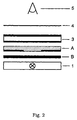
- FIG. 3 A an exploded schematic view of a possible device configuration is given.
- the arrangement when viewed from the position of the viewer ( 5 ) consists of a linear polarizer (analyzer) ( 4 ), an electrooptical light valve ( 3 ), the polarized PL layer ( 2 ) and a light source ( 1 ).
- Light emerging from the light-source ( 1 ) is at least partially absorbed in the polarized PL layer ( 2 ), from where subsequently polarized light Is emitted.
- the portion of the light emitted from the polarized PL layer ( 2 ) in the direction of the electrooptical light valve ( 3 ) either passes the combination of light valve ( 3 ) and the polarizer ( 4 ) (switching state “bright") or is blocked by the combination of light valve ( 3 ) and the polarizer ( 4 ) (switching state "dark”).
- switching states "bright” and “dark” not necessarily coincide with above referred electric switching states “on” and “off”, respectively, and the correlation also depends on the precise device configuration.
- the polarizer ( 4 ) is oriented such that it allows transmission of the light emitted by the polarized PL layer ( 2 ) in its polarization direction when the switching state of the light valve ( 3 ) is "bright".
- maximum contrast is obtained when (i) the polarized PL layer ( 2 ) is characterized by a high dichroic ratio for PL emission, and (ii) the portion of light visible to the human eye that is emitted by the light source ( 1 ), but not absorbed by the polarized PL layer ( 2 ), and thus exits the device in the direction of the viewer, is minimal, This can be achieved by different means.
- One example comprises a light source ( 1 ) which is characterized by an emission spectrum such that all the light emitted by the light source is absorbed by either the polarized PL layer ( 2 ), the light valve ( 3 ) or the polarizer ( 4 ).
- the use of a UV-light source can be particular advantageous in this context, since the portion of light that is emitted by the light source ( 1 ), but not absorbed by the polarized PL layer ( 2 ), is in this case usually absorbed by components ( 2 ), ( 3 ), or ( 4 ).
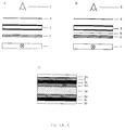
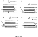
- FIG. 3 B An alternative example of a possible display device according to the present invention is shown in Fig. 3 B in an exploded schematic view.
- an additional means ( 8 ) (for clarity called “cut-off-filter"), which blocks the light that is emitted by the light source ( 1 ), but is not absorbed by the polarized PL layer ( 2 ), is positioned in the device between the polarized PL layer ( 2 ) and the viewer ( 5 ), preferably between the PL layer ( 2 ) and the light valve ( 3 ).
- This cut-off-filter ( 8 ) preferably is a wavelength-selective mirror which reflects the light generated by the lamp that was not absorbed by the polarized PL layer, but transmits the light emitted by the polarized PL layer or can, for example, be a high-pass filter or a polarizer or a combination thereof.
- Another preferred arrangement is the use of a combination layer of the polarized PL layer ( 2 ) and the cut-off-filter ( 8 ), for example, by doping or coating the polarized PL layer ( 2 ) with an additional dye.
- the display device can also be arranged, such that the polarized PL layer ( 2 ) is placed inside the electrooptical light valve ( 3 ), such as shown in an exploded schematic view in Fig. 3 C.
- the polarized PL layer ( 2 ) is positioned between the transparent electrode ( 3 c) and carrier plate ( 3b ).
- Particular advantages of this arrangement are a more compact device and an enhanced viewing angle, as well as the absence of parallax in a pixellated structure.
- the polarized PL layer ( 2 ) according to the present invention may function also as orientation layer ( 3d in Fig. 3 C) for the liquid crystalline material.
- the polar axis of the polarizer is the direction of the electrical field vector of the light that is transmitted by the polarizer films.
- the polarized PL layer axis is the direction of the electrical field vector of the light emitted by the polarized PL layer and which commonly, but not necessarily, is parallel to the direction of the electrical field vector of the excitation light that is absorbed .
- the polarizer film When these layers are placed in series with their axes crossed, the polarizer film will absorb the light generated by the polarized PL layer. In contrast, when placed parallel, the polarizer film transmits the light generated in the polarized PL layer.
- the liquid crystal cell is optimized to switch light of the wavelength of the light that is emitted by the polarized PL layer.
- the transmission is controlled by the axes of the polarized PL layer and the polarizer film, the switching state of the device field-off or -on state, the wavelength of the emitted light, the cell thickness and the optical properties of the LC material.
- the set of parameters are given below:
- the effective ⁇ n becomes smaller and the transmitted light becomes elliptically polarized.
- the polarizer film will now absorb part of the light, an effect that may be applied to generate intermediate tones.
- d ⁇ n / ⁇ becomes 0 and the light is fully extinguished by the polarizer ("dark" state).
- the axes of the polarizer and the polarized PL layer are chosen to be parallel, by which a dark field-off state and a bright and colored field-on state is obtained.
- the LC molecules have a negative dielectric anisotropy and are aligned perpendicular to the electrode surface by a surfactant type of alignment layer (e.g. lecithin).
- a surfactant type of alignment layer e.g. lecithin
- the LC film In the field-off state the LC film has a low birefringence for the passing light and a dark state is formed in case of crossed axes of the polarized PL layer and the polarizer film, respectively.
- the LC film becomes birefringent above the transition voltage, and the polarizer transmits the by the polarized PL layer emitted light.
- TN effect In the case that a multi-color display is made, containing pixel elements with basically three different polarized PL layers emitting blue, green and red light (see below), the TN effect is preferred because of its high contrast and its relative wavelength independence. This enables effective switching of the three colors with one uniform cell thickness.
- I t sin 2 ⁇ 2 1+ 2 d ⁇ n ⁇ 2 1+ 2 d ⁇ n ⁇ 2
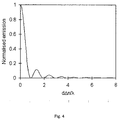
- the optimum cell thickness is 3.6 ⁇ m.
- the cell is perfectly black in the field-off state for 510 nm light and that it has a normalized emission of 0.08 for 440 nm light (blue) and of 0.06 for 620 nm light (red). Both values are sufficiently low to give the display a black appearance for all three colors.
- the axes of the polarized PL layer and the polarizer film can be chosen perpendicular.
- the inverted curve in Fig. 4 is obtained with a "bright" state, i.e. an emissive colored state for each pixel element and a white state for the integrated performance of a collection of neighboring pixels in the field-off state and a black appearance in the field-on state.
- a dichroic mirror ( 6 ) which is positioned between the polarized PL layer ( 2 ) and the light source ( 1 ), is advantageous (Fig. 3 D for an exploded schematic view).
- This dichroic mirror ( 6 ) is characterized in that it lets the light emitted by the light source ( 1 ) pass and reach the polarized PL layer ( 2 ), but reflects the portion of light which initially is emitted by the polarized PL layer ( 2 ) in a direction away from the viewer ( 5 ) and thus redirects this portion of light in the direction towards the viewer ( 5 ).
- the polarized PL layer ( 2 ) might, in addition, be mirrored ( 7 ) in order to prevent the exit of light in undesired directions and might be provided with light emergent or exit windows such as described in German patent No. DE 2640909 C2, to further concentrate the emission of light to preferred sites, and thus increase the device efficiency with respect to contrast and brightness.
- the polarized PL layer functions as a polarizing photoluminescence waveguide ( 10 ), in which the light emitted by the light source ( 1 ) is waveguided until it is absorbed and re-emitted by the photoluminescent moieties.
- the device is preferably fitted with a dichroic mirror ( 6 ) as outlined above, and with mirrors ( 7 ) and light emergent or exit windows as outlined above.
- a conventional waveguide-based backlight system is used (cf. Fig 3 F) in which the polarized PL layer ( 2 ) is arranged such that it is behind the waveguide ( 11 ) when viewed from the direction of the viewer ( 5 ).
- the waveguide ( 11 ) is characterized in that it emits the light guided from the light source ( 1 ) preferably into the direction of the polarized PL layer ( 2 ), and that it allows the transmittance of the polarized light emitted from the polarized PL layer ( 2 ).
- the polarized PL layer ( 2 ) in the display device according to Fig. 3 F may additionally function as a polarized scatterer or diffuser.
- ambient light ( 1 ) is used for illumination, entering the device in a direction from the viewer to the device, with the polarized PL layer ( 2 ) being void of mirrors on its two large faces (oriented towards the viewer and away from the viewer), but preferably mirrored ( 7 ) at all other sides.
- a dichroic mirror ( 6 ) is used, which only reflects the polarized light emitted by the the polarized PL layer ( 2 ).
- the ambient light which is not absorbed by the polarized PL layer ( 2 ) is absorbed in a nonreflective layer ( 9 ).
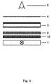
- Still another preferred arrangement according to the present invention is the use of two polarized PL layers ( 2 , 12 ), for example shown in an exploded schematic view Fig. 5.
- the two polarized PL layers ( 2 , 12 ) are characterized in that they have different emission spectra.
- These two polarized PL layers ( 2 , 12 ) may be arranged behind each other, when viewed from the direction of the viewer ( 5 ), positioned in the same place as the one polarized PL layer ( 2 ) in the above described arrangements.
- These two polarized PL layers ( 2 , 12 ) may be oriented such that their polarization directions for emission are perpendicular to each other.
- the combination of light valve ( 3 ) and the polarizer ( 4 ) no longer switches from bright to dark but lets the emitted polarized light from polarized PL layer ( 2 ) pass in the one switching state and the emitted polarized light from polarized PL layer ( 12 ) pass in the other switching state, enabling the production of a multicolor display device.
- the two polarized PL layers ( 2 , 12 ) may be oriented such that their polarization directions for emission are at an angle different from 90° to each other The latter arrangement enables switching between different multiple colors.
- the two polarized PL layers may be separated by the electrooptical light valve, or may be placed inside the electrooptical light valve (cf. Fig. 3 C).
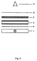
- FIG. 6 an exploded schematic view of a possible device structure is shown.
- the display device is arranged, such that the polarized PL layer is positioned between the electrooptical light valve ( 3 ) and the viewer.
- the polarizer ( 4 ) must be active in the wavelength region of the excitation wavelength.
- the particular advantage of switching this wavelength is that the LC cell can be optimized for a single wavelength regime (i.e. the excitation wavelength, for example UV) which leads to higher contrast values.
- the viewing angle is determined by the emission of the polarized PL layer and has become independent of the viewing angle-sensitive LC effects.
- 365 nm light is used for the excitation of the polarized PL layer ( 2 ).
- the optimum cell thickness is 2.1 ⁇ m.
- the polarized PL layer only absorbs light with its E-field parallel to the axis, the opposite polarization is transmitted.
- the previously described cut-off filter ( 8 ) may be used.
- two of such layers are present where the order is, coming from the backlight into the viewer's direction, a wavelength-selective mirror and a high-pass filter, respectively.
- the high-pass filter also contains other absorbing species which have a low absorption at the emission wavelength or wavelengths, but absorb visible light outside that wavelength region, thus even more improving the contrast by absorption of the light coming from the surroundings.
- an array of at least three different polarized photoluminescence pixel elements may be applied at or within the LC cell.
- the LC material within each pixel element can be addressed separately by an active or a passive electrode matrix.
- the polarized PL pixel elements are applied within the cell, for instance in between the transparent carrier plate and the transparent electrode. In another preferred embodiment the polarized PL pixel elements are applied outside the cell.
- the polarized PL pixels are applied in the cell near the LC film to avoid parallax and at the side of the viewer in order to improve the display on its viewing angle characteristics.
- Emission of white light from the display device is obtained by a balanced emission of the R, G and B pixel elements. Colors are generated by balanced mixing of the light emission of the various pixel elements.
- UV light preferably UV light of, for instance, 365 nm is used to excite the polarized PL layers.
- the appropriate white point can be obtained by adjusting the thickness of the polarized PL pixels, the concentration of the active photoluminescent moieties or the surface areas of the pixel elements.
- pixel elements In another pixillated display configuration three different pixel elements are made, two of them are provided with a red and a green emitting polarized PL layer, respectively that are exited by blue light.
- the third pixel element is provided with a neutral polarizing filter. In this case blue light is used from a backlight source.
- R and G are obtained from the polarized PL layers, B from the third pixel element by switching it to the "bright" or to the "dark" state.
- the blue pixel elements are not covered separately by the polarizer, but a polarizer film is used which covers all pixel elements.
- the axis of the polarizer is parallel to that of the polarized PL layers.
- the top polarizer absorbs that part of the light that otherwise would be reflected from the viewer's side.
- the black matrix can consist of organic material comprising a UV absorbing dye. This absorbing matrix can be applied using, for example, simple printing or lithographic techniques.
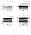
- One pixel element is able to generate multiple color if several polarized PL layers are combined as already shown above.
- two polarized PL layers are placed on top of each other, i.e. in a stacked fashion, with their axes perpendicular as shown in an exploded schematic view for a blue ( 2a ) and a red ( 2b ) emissive polarized PL layer in Fig. 7 A.
- the arrows in this Fig. 7 indicate the direction of the axes.
- the TN-type electrooptical light valve ( 3.1 ) controls the direction of the polarization of the excitation light.
- angles between the axes of the polarized PL layers other than 90° are possible in order to create special effects, or to combine, for instance, three different polarized PL layers. In that case the optical retardation of the polarized PL layer itself should also be accounted for, which might change the state of polarization of transmitted light.
- a preferred embodiment according to the present invention is shown in an exploded schematic view in Fig. 7 B.
- a combination of a dichroic mirror ( 14 ) which is reflective, for example, in the UV range and transmissive in the visible regime, and a quarter wave optical retardation film ( 13 ) can be utilized to address both colors separately.
- a polarizer active in the UV regime ( 4a ) excites the red polarized photoluminescence layer ( 2a ), while in the switching state "off” this polarized UV light is transmitted by the red polarized PL layer ( 2a ) and also by the blue one ( 2b ). However, upon reflection at the dichroic mirror ( 14 ) the polarization of the UV light is rotated and becomes absorbed and converted by the blue polarized PL layer ( 2b ).
- FIG. 7 C Another example of a preferred embodiment according to the present invention that allows display of mixed colors, intermediate tones and a dark state, is shown in an exploded schematic view in Fig. 7 C.
- different polarized PL layers ( 2b , 2c ) are addressed by separate, for example, TN-type electrooptical light valves ( 3.1 , 3.2 ).
- This configuration allows for a number of different possibilities, of which in the following two examples are given.
- the first example includes the use of a UV light source ( 1 ) and also makes use, as discussed for various examples before, of a cut-off filter (not shown in the figure) between the green polarized PL layer ( 2c ) and the viewer ( 5 ) that prevents the exit of UV excitation light in the direction of the viewer. Possible switching states and colors as observed by the viewer ( 5 ) are then: Situation # Electrooptical light valve ( 3.1 ) Electrooptical light valve ( 3.2 ) Observation by viewer ( 5 ) 1 Field on Field off Red emission 2 Field off Field on Green emission 3 Field off Field off No emission (dark)
- Intermediate tones and dark can be created in this configuration by a third TN electrooptical light valve and an additional polarizer (not shown in the figure), both positioned between the polarizer ( 4 ) and the light source ( 1 ), which modulates the intensity of the blue light.
- the double cell configuration is combined with a stack of polarized PL layers ( 2a , 2b , 2c ) with crossed axes as shown in Fig. 7 D.
- a third TN electrooptical light valve and an additional polarizer not shown in the figure, both positioned between the polarizer ( 4 ) and the light source ( 1 ).
- Another electrooptical light valve concept making use of the benefits of the polarized PL layers, is based on the so-called guest-host (GH) liquid crystal system.
- GH guest-host
- a dichroic dye added to the switching liquid crystal material, avoids the use of an additional polarizer or analyzer film.
- a dichroic dye absorbing in the wavelength region of the excitation wavelength is mixed with an ECB liquid crystal.
- the long axis of the dichroic dye organizes parallel to the liquid crystal molecules.
- the director axis of the liquid crystal is chosen to be parallel to the optical axis of the polarized PL layer. In the field-off state, one polarization direction of the excitation light becomes preferably absorbed by the dye and the polarized PL layer is not excited.
- the LC film In the field-on state, the LC film is completely transparent for the excitation light and the polarized PL layer emits light. In this embodiment only one polarization direction of the excitation light is used. Again, improvement of the light yield or brightness is obtained by adding a selective mirror which reflects in the wavelength region of the excitation light and transmits the emitted light.
- double cell arrangements can be beneficially used.
- the excitation light with the polarization that is transmitted by the first guest-host cell/polarized PL layer combination is switched by a second guest-host cell with its orientation axis perpendicular to that of the first one.
- a polarized PL layer is positioned which emits light with a different wavelength than that of the first polarized PL layer. In this way, two colors can be generated with one pixel element, thus improving the brightness and the color saturation of the display.
- the guest-host cells are placed on top of each other with their axes perpendicular. On top of these cells, the stack of polarized PL layers is positioned, also with their axes crossed. Each GH cell addresses one polarized PL layer of which the intermediate tone is controlled by the applied voltage over the cell. Bringing the GH cells in contact which each other has advantages with respect to cell manufacturing, electrical contacts and device thickness.
- a guest-host and a TN electrooptical light valve are combined.
- the light that is transmitted by a first GH-electrooptical light valve/polarized PL layer combination is automatically polarized. This polarization can be utilized to switch the second polarized PL layer with a TN effect.
- Embodiments of preferred display devices that comprise other electrooptical light valves, such as those based on, for example, super-twisted nematics, in-plane nematic and ferroelectrics, or combinations thereof, are also included in the present invention.
- light that is emitted from one polarized PL layer can be used for the excitation of another polarized PL layer leading to additional improvements and enhanced device characteristics.
- the display devices according to the present invention may optionally include one or more additional layers or elements including, but not limited to diffusers, color filters, scatterers, and/or prismated films.
- the elements constituting the display devices should have photophysical characteristics, such as transmission, absorption and refractive index, that are optimized with respect to the emission wavelength and other optical characteristics of the polarized PL layers of the present invention, and also the light source, according to the principles well known to those skilled in the art of display device design and manufacturing.
- Polymers designated, respectively, O-OPPE, substituted with only linear alkyloxy side chains, and EHO-OPPE, derivatized with linear and sterically hindered alkyloxy groups in an alternating pattern are of the following chemical structures: These substituted poly(phenyleneethynylene)s (PPEs) were synthesized according to the procedures described in Ch. Weder et al., Macromolecules, (1996) Vol. 29, p. 5157, and D. Steiger et al., Makromol. Chem. Phys., Rapid Comm., in press.
- Thin blend photoluminescent layers with contents of 1 and 2 % w/w of PPE were prepared by casting a solution of the different PPEs (5 or 10 mg) and ultra-high molecular weight polyethylene (UHMW PE, Hostalen Gur 412. Hoechst AG) (0.5 g) in xylene (50 g) (dissolution at 130 °C after degassing the mixture in vacuum at 25°C for 15 min.) into a petri-dish of 11 cm in diameter. The resulting gel layers were dried under ambient conditions for 24 h. These unoriented blend layers had a homogeneous thickness of about 70 ⁇ m.
- the oriented layers had a thickness in the range from about 1 to about 10 ⁇ m.
- thin blend layers with a content of 1% w/w of MEH-PPV were prepared by casting a solution of the MEH-PPV and ultra-high molecular weight polyethylene (UHMW PE, Hostalen Gur 412, Hoechst AG) in the identical manner as described above.
- UHMW PE ultra-high molecular weight polyethylene
- thick photoluminescent plates with a content of 1 % w/w of PPE were produced by first casting a solution of EHO-OPPE (20 mg) and high molecular weight polyethylene (HMW-PE, Hostalen GR 7255, Hoechst AG, M w of ⁇ 400,000 g mol -1 ) (2 g) in xylene (200 g) (dissolution at 135 °C after degassing the mixture in vacuum at 25°C for 15 min.) into a petri-dish of 11 cm in diameter. The resulting gels were dried for 70 h at ambient.
- EHO-OPPE 20 mg
- HMW-PE high molecular weight polyethylene
- Hostalen GR 7255 Hoechst AG
- M w of ⁇ 400,000 g mol -1 2 g
- xylene 200 g
- the resulting gels were dried for 70 h at ambient.
- the obtained blend was collected, placed between two aluminium plates, fitted with 1 mm spacers, and melt-pressed in a hot press for 5 min at temperatures of 140 - 150 °C under a pressure of 3-5 metric tons to yield plates of a thickness of approximately 1 mm.
- One plate was drawn at a temperature of 120 °C in an Instron tensile-tester equipped with a thermostatic chamber, to yield an oriented plate of a draw-ratio of 3.6 and a thickness of 1.5 mm.
- the anisotropic photophysical behavior of these oriented layers and plates was analyzed with polarized photoluminescence (PL) and polarized UV/Vis absorption spectroscopy.
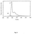
- PL photoluminescence
- UV/Vis absorption spectroscopy For the photophysical analysis, the polymer layers and plates were sandwiched between two quartz slides; silicon oil fluid was applied in order to minimize light scattering at the layer and plate surfaces. The dichroic ratios were measured as defined above.
- PL spectra were recorded on a SFEX Fluorolog 2 (Model F212 1), using unpolarized light (350 nm) for excitation and a Glan-Thomson polarizer on the detector side.
- UV/Vis absorption spectra were recorded on a Perkin Elmer Lambda 900 instrument, fitted with motor driven Glan-Thomson polarizers. Scattering effects were compensated in the absorption measurements by subtracting the spectra of pure UHMW PE films of comparable draw ratio and thickness.
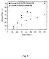
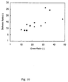
- the 80 times drawn layer containing 1 % MEH-PPV displayed a dichroic ratio, measured in emission, of 62.
- the oriented plate of a draw ratio of 3.6 and a thickness of 1.5 mm was characterized by a dichroic ratio, measured both in emission and absorption, of only about 2.
- a display device was constructed according to the schematic of Fig. 3 A.
- a UV lamp Bioblock, VL-4LC, 4 Watts
- 365 nm was employed as a light source.
- an unoriented, thick polymer blend plate of 1 mm thickness of HMW PE containing 1 % w/w of EHO-OPPE prepared according to Example A was placed in between the UV source and a commercial liquid crystal display, consisting of a patterned electrooptical light valve ( 3 ) and one absorbing polarizer ( 2 ), arranged as shown in Fig 3 A.
- Selected patterns of the display device were switched between the "on” and the "off” state, but the switching did not change the appearance of the device. Due to the isotropic emission from the unoriented plate, the entire area was illuminated by the light source, and the device in both switching states showed a dim, continuous, homogeneous yellow-green light.
- This comparative example shows that employing a thick, unoriented plate of photoluminescent material, characterized by a dichroic ratio of unity in absorption and emission, in a device configuration according to Fig. 3 A, does not yield a display device, that can be switched between two different optical states ("bright” and "dark”).
- Example B (Outside of the Invention) was repeated, but instead of an unoriented, polymer blend plate of 1 mm thickness of HMW PE containing 1 % w/w of EHO-OPPE, a 70 ⁇ m thin, unoriented layer of UHMW PE containing 1 % w/w of EHO-OPPE (prepared according to Example A) was used in the device. Selected patterns of the display device (segments) were switched between the "on” and the "off” state, but the switching did not change the appearance of the device. Due to the isotropic emission from the unoriented layer, the entire area was illuminated by the light source, and the device in both switching states showed a continuous, homogeneous yellow-green light.
- This comparative example shows that employing a thin, unoriented layer of photoluminescent material, characterized by a dichroic ratio of unity in absorption and emission, in a device configuration according to Fig. 3 A, does not yield a display device, that can be switched between two different optical states ("bright” and "dark”).
- Example B (Outside of the Invention) was repeated, but instead of an unoriented, polymer blend plate of 1 mm thickness of HMW PE containing 1 % w/w of EHO-OPPE, a 1.5 mm thick, oriented plate of the same composition, of a draw-ratio of 3.6 and a dichroic ratio, measured in emission and absorption, of about 2 (prepared according to Example A) was used in the device. Selected patterns of the display device (segments) were switched between the "on” and the "off” state. The switching, indeed, led to a change in brightness, but however, the contrast between the "on” and the "off” state, as perceived by the human eye, was extremely low. One reason for the poor contrast of this device is the fact that the switched segments in their "off” state still exhibit a significant yellow-green emission.
- This comparative example shows that employing a thick photoluminescent plate with a moderate polarized absorption and emission does not yield significantly improved characteristics of a liquid crystal display.
- Example B (Outside of the Invention) was repeated, but instead of an unoriented, polymer blend plate of 1 mm thickness of HMW PE containing 1 % w/w of EHO-OPPE, an oriented, about 30 ⁇ m thin polymer blend layer of UHMW PE containing 1 % w/w of O-OPPE of a draw ratio of about 5 and a dichroic ratio, measured in absorption, of about 3.8 (prepared according to the methods described in Example A), was used in the device. Selected patterns of the display device (segments) were switched between the "on” and the "off” state. The switching, indeed, led to a change in brightness, but however, the contrast between the "on” and the "off” state, as perceived by the human eye, was extremely low. One reason for the poor contrast of this device is the fact that the switched segments in their "off” state still exhibit a significant yellow-green emission.
- This comparative example shows that employing a thin photoluminescent layer with a moderate polarized absorption does not yield significantly improved characteristics of a liquid crystal display.
- a display device was constructed according to the schematic of Fig. 3 A.
- a UV lamp (Bioblock, VL-4LC 4 Watts), operated at 365 nm, was employed as a light source. (It should be noted that the latter was not optimized for the particular absorption band of the present photoluminescent materials).
- the polarized PL layer ( 2 ) was a highly oriented, 2 ⁇ m thin polymer blend layer of UHMW PE containing 2 % w/w of EHO-OPPE of a draw ratio of 80 and a dichroic ratio, measured in absorption, of 16, and, measured in emission, of 72 (prepared according to Example A), and was placed in between the UV source and a commercial liquid crystal display, consisting of a patterned electrooptical light valve ( 3 ) and one absorbing polarizer ( 2 ), arranged as shown in Fig 3 A. Selected patterns of the display device (segments) were switched between the "on” and the "off” state.
- the switching yielded a significant change in brightness, that was perceived by the human eye as a change from a very bright yellow-green to almost dark.
- the absolute brightness of the "on” and the "off” state were measured with a Minolta LS 100 luminance meter, which was fitted with a No 110 and a No 122 close-up lens.
- the contrast ratio which hereinafter is defined as the ratio between the brightnesses of the "on” and "off” state, of the device was in excess of 7. For the commercial direct-view LCD the contrast ratio was about 3.5.
- This example shows that employing a thin, polarized PL layer characterized in a high degree of polarization for both, absorption and emission, yields a liquid crystal display of dramatically improved contrast.
- Example 1 was repeated, but instead of the drawn blend film containing 2 w/w % of EHO-OPPE in UHMW PE, an 80 times drawn blend film containing 1 w/w % MEH-PPV in UHMW PE with a dichroic ratio, measured in emission, of 62, prepared according to Example A, was used. Selected patterns of the display device (segments) were switched between the "on” and the "off” state. The switching yielded a significant change in brightness, that was perceived by the human eye as a change from a orange-red to almost dark. The contrast and absolute brightness of the "on” and the "off” state of the device were comparable to the device in Example 1.
- a display device was constructed according to the schematic of Fig. 5.
- a UV lamp (Bioblock, VL-4LC, 4 Watts), operated at 365 nm, was employed as a light source. (It should be noted that the latter was not optimized for the particular absorption bands of the present photoluminescent materials).
- the two polarized PL layers ( 2 , 12 ), were an oriented, 2 ⁇ m thin polymer blend layer of UHMW PE containing 2 % w/w of EHO-OPPE of a draw ratio of 80 and a dichroic ratio, measured in absorption, of 16, and, measured in emission, of 72 ( 2 ) and an oriented, 2 ⁇ m thin polymer blend layer of UHMW PE containing 1% w/w MEH-PPV of a draw ratio of 80 and a dichroic ratio, measured In absorption, of 14, and, measured in emission, of 62 ( 12 ) (prepared according to Example A).
- the polarized PL layers ( 2 , 12 ) were placed with their orientation directions perpendicular to one another and in between the UV source and a commercial liquid crystal display, consisting of a patterned electrooptical light valve ( 3 ) and one absorbing polarizer ( 2 ), arranged as shown in Fig 5. Selected patterns of the display device (segments) were switched between the "on” and the "off” state. The switching, led to a significant change in color, that was perceived by the human eye as a change from a bright yellow-green to orange-red.
- a commercial liquid crystalline mixture (K15, BDH Ltd.) was placed onto the 80 times drawn blend films containing 2 % w/w of EHO-PPE in UHMW PE and containing 1 % w/w MEH-PPV in UHMW PE, respectively, prepared according to Example A were used.
- the liquid crystalline material was found to immediately adopt a uniaxial orientation.
- This example shows that the layers according to the present invention also can be placed inside a liquid crystal cell that operates as a light valve in a display device, and functions not only as the polarized PL layer but also as orientation layer ( 3d in Fig. 3 C) for the liquid crystalline material.
Landscapes
- Physics & Mathematics (AREA)
- Nonlinear Science (AREA)
- Mathematical Physics (AREA)
- Chemical & Material Sciences (AREA)
- Crystallography & Structural Chemistry (AREA)
- General Physics & Mathematics (AREA)
- Optics & Photonics (AREA)
- Polarising Elements (AREA)
- Liquid Crystal (AREA)
- Devices For Indicating Variable Information By Combining Individual Elements (AREA)
Abstract
Display devices are disclosed of a high brightness, high contrast and
large viewing angle that comprise at least one thin, photoluminescent
layer (2) that is characterized in a high degree of polarization in its
absorption.
Description
The present invention relates to display devices and in
particular to displays comprising at least one photoluminescent layer
that is characterized in a high degree of polarization in its
absorption.
Optoelectronic display devices, such as those based on the
Electrically Controlled Birefringence (ECB) effect, the Twisted
Nematic (TN) effect and Super-Twisted Nematic (STN) effect (S. W.
Depp et al., Sci. Am., Vol. 268, p. 40 (1993); T. Scheffer et al., in
"Liquid Crystals, Applications and Uses", Vol. 1, B. Bahadur, Ed.,
Chapter 10, pp. 231-274 (1990), Worlds Scientific, Singapore; S.
Morozumi, ibid., Chapter 7, pp. 171-194), are well known in the art
and are of major importance in a large variety of applications.
In these devices (cf. Fig. 1 A), typically, a liquid crystalline
material is sandwiched in a cell (3) between two light-polarizing
means (4) and the liquid crystalline material is used to electrically
rotate the polarization direction of polarized light and, thus, the
structure functions as a light valve. Polarized light is produced in
these devices by a first polarizer, and a second polarizer (also
referred to as analyzer) is used to generate visual perception of the
electrical switching of the liquid crystalline material.
As is well established in the prior art, a thin layer of well-ordered
liquid crystalline material has the ability to change the state
of polarization of light that passes through it. As the LC order can be
controlled by means of an electrical field, electric switching can
modulate the polarization of the transmitted light. Thereto, typically,
a cell structure (cf. Figs. 1 A, B), based on spacered transparent
carrier plates (3b) and provided with two transparent electrodes
(3c), is utilized where in between the thin layer of LC material (3a) is
applied. The transparent electrode material can be, for instance,
indium tin oxide, but may also consist of a transparent conducting
polymer. In the field-off state, or at low voltages below a threshold
value (switching state "off"), the molecular organization within the
liquid crystal layer is planar and well-controlled by orientation layers
(3d) applied on the electrodes and/or by the presence of small
amounts of chiral dopants in the liquid crystal mixture. Well-known
and widely used effects are: (i) Electrically Controlled Birefringence
(ECB) effect in which the molecules are aligned unidirectionally
(parallel alignment at the orientation layers, no chiral dopant); and
(ii) twisted nematic (TN) or super-twisted nematic (STN) effects in
which the molecules are rotated over, for instance, 90° (TN) by
means of a perpendicular alignment at the orientation layer. In the
field-on state (switching state "on"), the LC molecules align
themselves along the electrical field lines. In the limit, i.e. at the fully
addressed state at higher voltages, the LC material is aligned
perfectly perpendicular to the electrode surfaces and behaves
isotropically for the light which passes parallel to the field lines. This
means that the state of polarization of light that passes the cell
remains unaffected. At intermediate voltages also intermediate states
of orientation can be achieved in which the director, being the local
direction of the average orientation of the LC molecules, describes a
complicated pattern over the thickness of the cell, which can be
used to create intermediate scales between the fully-off and the fully-on
state.
When these devices comprise only conventional absorbing
polarizers, they change upon switching from a light grey to a dark
appearance. Colors are generated by using, for example, additional
color filters (US Patent 5,099,345) or a series of selective dichroic,
filtering polarizers (US Patent 5,122,887).
A common dichroic sheet polarizer usually absorbs at least 50
% of the incident light. In a typical TN display, more than 80 % of
the incident light is absorbed by the polarizers and color filters and,
consequently, the brightness of the displays is very limited. The poor
light efficiency of these displays, generally, is compensated by rather
intense backlighting which limits the life-time of batteries in
devices such as lap-top computers and portable telephones.
Moreover, conventional polarizers transfer the absorbed light into
heat and, consequently, exhibit excessive heating-up when used in
combination with high-intensity light sources. These high-intensity
light sources are employed in applications such as projection
televisions, and the polarizers limit the life-time of the displays in
these applications.
The use of photoluminescent, for example fluorescent or
phosphorescent, matter to overcome these problems has been
described. For example, US Patent 3,844,637 discloses the use of
fluorescent liquid crystals. Fluorescent material dissolved or
dispersed in liquid crystals also has been suggested (US Patent
4,336,980; H. J. Coles et al., Liq. Cryst., Vol. 14, pp. 1039-1045
(1993)). The use of fluorescent particles as a light trap was described
in US Patent 4,405,210. US Patent 4,470,666 discloses the use of a
partially transmissive fluorescent color filter. US Patent Nos.
4,113,360, 4,394,068 and 5,018,837, W. Greubel et al. (Elektronik,
Vol. 6., pp. 55-56 (1977)) and M. Bechtler et al. (Electronics,
December 8, pp. 113-116 (1977)) describe the use of a plate of
fluorescent synthetic material in displays as a light trap. US Patent
5,608,554 describes the use of a phosphor layer to enhance the
luminance and viewing angle of standard liquid crystal display
devices. Also, the use of a layer comprising fluorescent species in the
three primary colors has been disclosed (French application FR 2
600 451 - A1; US Patent 4,678,285). German patent No. DE
2640909 C2 and G. Baur et al. (Appl. Phys. Lett., Vol. 31, pp. 4-6
(1977); W. Greubel et. al., Elektronik, pp. 55-56 (1977)) disclose a
display device that comprises an at least partially mirrored polymer
plate (cf. Fig. 2, (A)) in which a fluorescent dye is dissolved and that
further comprises a means (B) positioned behind the polymer plate
(A), from the light-exit direction, that allows transmission of only
that part of the light spectrum that is absorbed by the fluorescent
plate (A). Furthermore, in the same patent, which is directed
towards the use of a fluorescent plate as a light trap in displays, it is
suggested that a plate (A) can be used in which form-anisotropic
fluorescent molecules are dissolved in a uniform orientation within
the polymer plate. The proposed display configurations suffer a
number of drawbacks, most of which are directly related to the
dimensions of the plate. First, the light collection area of the
fluorescent plate must be substantially larger than the area of the
electrooptical light valve to provide enough of the necessary
radiation. These displays are therefore only suitable for applications
where there is enough room for such a plate such as measuring
instruments or digital clocks (M. Bechter et. al., Electronics,
December 8, pp. 113-116 (1977)). Secondly, according to other
publications by the authors of the prior art patent (G. Baur et al., Appl.
Phys. Lett., Vol. 31, pp. 4-6 (1977); W. Greubel et. al., Elektronik, pp.
55-56 (1977)) the fluorescent plate needs to be thick (> 1 mm) to
generate a high absorption of environmental light. According to the
authors, the dye concentration in the plate must be low to avoid
"self-absorption" and consequently the plate thickness must be high
to generate a light absorption close to 100 %. The absorption (A) of
the incident light on the surface of the plate is:
A = 1-10-ε(λ)ct
where ε(λ) is the molar extinction coefficient of the fluorescent dye
at wavelength λ, c is the molar concentration of the fluorescent dye
and t is the plate thickness. According to publications by the authors
of the prior art patent (G. Baur et al., Appl. Phys. Lett., Vol. 31, pp. 4-6
(1977); W. Greubel et. al., Elektronik, pp. 55-56 (1977)) typical
values for the extinction coefficient of the fluorescent dye and the
dye concentration are, respectively, 104 L/mole cm and 10-3 mole/L.
Consequently, a plate with a thickness of 1.5 mm is required to
generate an absorption of 97 % of the incident light, but also plates
thicker than 7.5 mm were fabricated and used (G. Baur et al., Appl.
Phys. Lett., Vol. 31, pp. 4-6 (1977); W. Greubel et. al., Elektronik, pp.
55-56 (1977)). Hence, the large thickness of the plates increases the
dimensions of the display devices also in the thickness direction. As
a consequence, thin or, for instance, flexible displays cannot be
manufactured. In addition, again according to G. Bauer et. al. (Appl.
Phys. Lett., Vol. 31, pp. 4-6 (1977)) the plates act as waveguides for
the fluorescent light and the light travels distances between 1 to 100
cm in the plate before it is coupled out. Consequently, the light
output (brightness) is strongly reduced by the overlap of the
absorption and emission spectrum of the fluorescent dyes. To
minimize other light losses, plates have to be produced from highly
transparent materials with perfect optical surfaces and perfectly
reflecting layers at the narrow sides are required.
Unfortunately, the above improvements have failed to yield
display devices which can be used in a large range of applications in
an economical and satisfactory way, and the need continues to exist
for more efficient displays of high brightness, high contrast, a wide
viewing angle, and optional multiple colors.
One object of the present invention to overcome the problems
of the prior art displays. Is to provide a display device that comprises
at least one thin, photoluminescent layer that is characterized in a
high degree of polarization in its absorption and that is characterized
by an emission which Is either polarized or not polarized.
Another object of the present invention it to provide a display
device that comprises one photoluminescent layer that is
characterized in a high degree of polarization in its absorption, and
one polarizer or analyzer.
Yet another object of the present invention it to provide a
display device that comprises a first photoluminescent layer that is
characterized in a high degree of polarization in Its absorption, and a
second photoluminescent layer that is characterized in a high degree
of polarization in its absorption, and that is further characterized in
that the two layers have different photoemission or absorption
spectra or both.
Still another object of the present invention is to provide a
display device that comprises multiple photoluminescent layers that
are characterized in a high degree of polarization in their absorption,
and multiple electrooptic light valves, arranged in a stacked fashion,
and that is further characterized in that the layers different
photoemission or absorption spectra or both.
Another object of the the present invention is to provide a
display device that comprises at least one thin, photoluminescent
layer that is characterized in a high degree of polarization in its
absorption and that is characterized by an emission which is either
polarized or not polarized and that is characterized by small
dimensions in the thickness direction and area.
Other objects of the present invention will become apparent to
those skilled in the art in the following detailed description of the
invention and the appended claims.
The present invention is based on our surprising finding that
display devices comprising at least one thin photoluminescent layer
that is characterized in a high degree of polarization in its absorption
are of a very high brightness and very high contrast, have an
excellent viewing angle, and can be configured to exhibit one or
more colors that cover the entire visible portion of the spectrum of
light useful for display applications. Hereinafter, the designation
photoluminescent and photoluminescence are abbreviated with the
designation PL, and further, the term polarized PL layer refers to a
photoluminescent layer that is characterized in a high degree of
polarization in its absorption and that is characterized in an emission
which is either polarized or not polarized. Most importantly, we
found that the polarized PL layers should be thin and should exhibit a
dichroic ratio that exceeds a minimum value in order to yield
displays with the above desired characteristics. Hereinafter, device
elements such as layer, electrooptical light valve, polarizer, light
source, and mirror are sometimes referred to in their singular form,
which should not be construed as to imply that reference is made to
only one such element.
Herein the dichroic ratio in absorption is defined as the ratio of
the highest possible absorption of linear polarized light to the
lowest possible absorption of linear polarised light. These
absorptions are measured at the same single wavelength somewhere
within the absorption spectrum and preferentially at an absorption
maximum.
Herein, the dichroic ratio in emission is defined as the highest
possible emission of linear polarized light to the lowest possible
emission of linear polarized light. These emissions are measured at
the same single wavelength using unpolarized excitation light at a
single wavelength somewhere within the emission spectrum and
preferentially at an emission maximum.
The above objects and advantages of the present invention will
become more apparent by describing in detail preferred
embodiments thereof with reference to the attached drawings in
which:
The present invention is based on our surprising finding that
display devices comprising at least one thin highly polarized PL layer
are of a very high brightness and very high contrast, have an
excellent viewing angle, and can be configured to exhibit one or
more colors that cover the entire visible portion of the spectrum of
light useful for display applications. Most importantly, we found that
the polarized PL layers should be thin and should exhibit a dichroic
ratio in absorption that exceeds a minimum value in order to yield
displays with the above desired characteristics.
The polarized PL layers useful in the present invention are
characterized in that they absorb light in a highly polarized fashion
and, after photoexcitation, they emit light that can be polarized or
not. Such polarized PL layers can comprise one or more different
substances, and can be manufactured by a wide variety of methods.
The substances to be selected and fabrication methods that are most
appropriate for the desired application form and color or colors of
the display device are known from the state of the art. To avoid any
replication from the known prior art, all the below mentioned
literature references in relation to appropriate substances and
methods of fabrication are herewith included in and part of the
present invention.
The polarized PL layers, for example, may comprise one or
more inorganic materials, such as GaInP-compounds (P. J. Pearah et
al. Appl. Phys. Lett. Vol. 62, pp. 729-731), ZnSe (L. Worschech et al.,
"Blue Laser Light Emitting Diodes", Int. Symp. pp. 421-424, Eds. A.
Yoshikawa, Tokyo, Japan, 1996), or tris(bipyridine)ruthenium(2+)
intercalated cadmiumthio-hypophosphazene (E. Lifshitz et al., J.
Phys. Chem. Solids, Vol. 52. pp. 1081-1086 (1991), or inorganic
oligomers or polymers, or mixtures thereof.
Alternatively, the polarized PL layers useful in the present
invention may comprise one or more organic species, such as small
molecules, oligomers or polymers, or mixtures thereof or of organic
and inorganic materials. Representative examples of small organic
species and oligomers useful in the present invention can be found
in, for example, "Organic Luminescent Materials" by B. M.
Krasovitskii et al. (VCH Verlag., Weinheim, 1988).
Oligomers and polymers that are useful in the present
invention include, but are not limited to those molecules that
comprise one or more of the following moieties:
 where Ar is an arylene group including, but not limited to the
following moieties:
where Ar is an arylene group including, but not limited to the
following moieties:
 and where R1 -R6, are the same or different at each occurrence, and
are composed of, for example, but not limited to: H, alkyl alkyloxy,
CF3, CN, phenyl NH2, NH-alkyl, N(alkyl)2, NO2 and Si(alkyl)3.
and where R1 -R6, are the same or different at each occurrence, and
are composed of, for example, but not limited to: H, alkyl alkyloxy,
CF3, CN, phenyl NH2, NH-alkyl, N(alkyl)2, NO2 and Si(alkyl)3.
Polarized PL layers for use in the present invention can be
made, for example, by incorporation of appropriate
photoluminescent, low molecular weight organic molecules or
inorganic matter in oriented polymers, prior to or after the
orientation step (J. J. Dekkers, Chem. Phys. Lett., Vol. 19, pp. 517-523
(1973); L. V. Natarajan et al., Chem. Phys. Lett., Vol. 95, pp. 525-528
(1983); R. Neuert et al., Colloid & Polymer Science, Vol. 263,
pp. 392-395 (1985); M. van Gurp et al., J, Polym. Sci., Part B,
Polymer Physics, Vol. 26, pp. 1613-1625 (1988); Y. Dirix et al.,
Macromolecules, Vol. 30, pp. 2175-2177 (1997); US Patent
4,56,953).
Another beneficial method for the fabrication of the polarized
PL layers for use in the present invention is tensile orientation if the
selected photoluminescent material is a ductile polymer (C. Zhang et
al., Synth. Met., Vol. 46, pp. 235-242 (1992); J. Moulton et al.,
Polymer, Vol. 33, pp. 2340-2348 (1992); P. Dyreklev et al., Adv.
Mater., Vol. 7, pp. 43-44 (1995); U. Lemmer et al., Appl. Phys. Lett.,
Vol. 68 pp. 3007-3009 (1996), or a ductile blend of
photoluminescent polymers or oligomers with carrier polymers (US
Patent 5,204,038; J. Moulton et al., J. Polym. Sci., Polym. Phys. Ed.,
Vol. 30, pp. 871-878 (1992)).
Alternatively, polarized PL layers useful in the present
invention can be fabricated by oriented growth of photoluminescent
materials onto orienting substrates, such as, for example, oriented
poly(tetrafluoroethylene) (US Patent 5,180,470; K. Pichler et al.,
Synth. Met., Vol. 55-57, pp. 454-459 (1993); D. Fenwick et al., J.
Mater. Sci., Vol. 31, pp. 915-920 (1996); R. Gill, et al., Adv. Mater.,
Vol. 9, pp. 331-334 (1997)), polyimides (G. Lüssem et al., Liq. Cryst.,
Vol. 21, pp. 903-907 (1996) or inorganic surfaces (P. J. Pearah et al.,
Appl. Phys. Lett. Vol. 62, pp. 729-731 (1993)).
Direct deposition through friction of photoluminescent
materials (N. Tanigaki et al., Thin Solid Films, Vol. 273, pp. 263-266
(1996) or rubbing of photoluminescent materials, or the Langmuir-Blodgett
technique (V. Cimrová et al., Adv. Mater., Vol. 8, pp. 146-149
(1996); A. Bolognesi et al., Adv. Mater., Vol. 9, pp. 121-124
(1997); M. Hamaguchi et al., Appl. Phys. Lett., Vol. 67. pp. 3381
(1995)) may also be employed for the fabrication of the polarized PL
layers for use in the present invention. Other techniques, such as
photo-induced alignment. alignment in electric, magnetic or flow
fields of photoluminescent substances that yield highly polarized PL
layers may also be employed.
Unlike the photoluminescent polymer plates of the prior art
which, of need, are thick, the polarized PL layers according to the
present invention are thin, and have a thickness of less than about
1 mm, preferably of less than about 300 µm, and more preferably of
less than about 50 µm. Most preferably, the thickness of the
polarized PL layers according to the present invention is less than
about 10 µm. The polarized PL layers according to the present
invention have a minimum thickness of at least 1 nm.
The dichroic ratio in absorption as defined above of the thin,
polarized PL layers for use in the present invention is more than
about 5. Preferably, the dichroic ratio is more than 10, and most
preferred are dichroic ratios of more than 20.
The polarized PL layers for use in the present invention may be
homogeneous and continuous, and may be structured or patterned,
and may comprise multiple individual elements, zones or pixels, or
any array thereof, provided, however, that the dichroic ratio of the
polarized PL elements are of the above minimum dichroic ratio.
Stacks of such polarized PL layers, for example for use in multiple
color displays, are also included in the present invention.
In the display devices according to the present invention, both
light from the light source employed for photoexcitation of the
polarized PL layer, and light emitted from the exited polarized PL
layer may be switched. Some of the relevant basic principles of the
display devices according to the present invention and preferred
embodiments, many of which may include either one of these
switching modes, are presented hereafter.
First presented are embodiments of display devices in which
the light emitted from the polarized PL layer is switched. In this
case, the predominantly relevant polarization characteristic of the
polarized PL layer is a high degree of polarized emission. In Fig. 3 A,
an exploded schematic view of a possible device configuration is
given. The arrangement, when viewed from the position of the viewer
(5) consists of a linear polarizer (analyzer) (4), an electrooptical light
valve (3), the polarized PL layer (2) and a light source (1). Light
emerging from the light-source (1) is at least partially absorbed in
the polarized PL layer (2), from where subsequently polarized light Is
emitted. The portion of the light emitted from the polarized PL layer
(2) in the direction of the electrooptical light valve (3) either passes
the combination of light valve (3) and the polarizer (4) (switching
state "bright") or is blocked by the combination of light valve (3) and
the polarizer (4) (switching state "dark"). It should be noted, that
the switching states "bright" and "dark" not necessarily coincide
with above referred electric switching states "on" and "off",
respectively, and the correlation also depends on the precise device
configuration. The polarizer (4) is oriented such that it allows
transmission of the light emitted by the polarized PL layer (2) in its
polarization direction when the switching state of the light valve (3)
is "bright". According to the present invention, maximum contrast
is obtained when (i) the polarized PL layer (2) is characterized by a
high dichroic ratio for PL emission, and (ii) the portion of light
visible to the human eye that is emitted by the light source (1), but
not absorbed by the polarized PL layer (2), and thus exits the device
in the direction of the viewer, is minimal, This can be achieved by
different means. One example comprises a light source (1) which is
characterized by an emission spectrum such that all the light emitted
by the light source is absorbed by either the polarized PL layer (2),
the light valve (3) or the polarizer (4). The use of a UV-light source
can be particular advantageous in this context, since the portion of
light that is emitted by the light source (1), but not absorbed by the
polarized PL layer (2), is in this case usually absorbed by components
(2), (3), or (4).
An alternative example of a possible display device according to
the present invention is shown in Fig. 3 B in an exploded schematic
view. Here, an additional means (8) (for clarity called "cut-off-filter"),
which blocks the light that is emitted by the light source (1),
but is not absorbed by the polarized PL layer (2), is positioned in the
device between the polarized PL layer (2) and the viewer (5),
preferably between the PL layer (2) and the light valve (3). This cut-off-filter
(8) preferably is a wavelength-selective mirror which
reflects the light generated by the lamp that was not absorbed by the
polarized PL layer, but transmits the light emitted by the polarized PL
layer or can, for example, be a high-pass filter or a polarizer or a
combination thereof. Another preferred arrangement is the use of a
combination layer of the polarized PL layer (2) and the cut-off-filter
(8), for example, by doping or coating the polarized PL layer (2) with
an additional dye.
The display device can also be arranged, such that the
polarized PL layer (2) is placed inside the electrooptical light valve
(3), such as shown in an exploded schematic view in Fig. 3 C. In
order to keep the switching voltages low, the polarized PL layer (2)
is positioned between the transparent electrode (3c) and carrier
plate (3b). Particular advantages of this arrangement are a more
compact device and an enhanced viewing angle, as well as the
absence of parallax in a pixellated structure. In addition, the
polarized PL layer (2) according to the present invention, may
function also as orientation layer (3d in Fig. 3 C) for the liquid
crystalline material.
To define the operation of the devices that can be built based
on this configuration, a definition is given of the several axes that will
be used:
The polar axis of the polarizer is the direction of the electrical
field vector of the light that is transmitted by the polarizer films.
The polarized PL layer axis is the direction of the electrical field
vector of the light emitted by the polarized PL layer and which
commonly, but not necessarily, is parallel to the direction of the
electrical field vector of the excitation light that is absorbed.
When these layers are placed in series with their axes crossed, the
polarizer film will absorb the light generated by the polarized PL
layer. In contrast, when placed parallel, the polarizer film transmits
the light generated in the polarized PL layer.
For the above given configuration (except display devices
comprising the polarized PL layer (2) inside the electrooptical light
valve (3) as shown in Fig. 3 C, arranged such that light emerging from
the light source first passes the liquid crystal layer (3a) before
exciting the polarized PL layer (2)), the liquid crystal cell is
optimized to switch light of the wavelength of the light that is
emitted by the polarized PL layer. The transmission is controlled by
the axes of the polarized PL layer and the polarizer film, the
switching state of the device field-off or -on state, the wavelength of
the emitted light, the cell thickness and the optical properties of the
LC material. For some LC effects the set of parameters are given
below:
ECB effect: When the polar axis of the polarizer and the
polarized PL layer axis are crossed and the liquid crystal orientation
is at 45° with these axes, the maximum transmission ("bright" state)
in the field-off state depends on the thickness of the cell d, the
birefringence of the liquid crystal Δn and the wavelength λ and
occurs at
d Δn λ = k 2 with k = 1, 3, 5, 7, .....
In that case, the polarized light transmitted by the LC layer remains
linearly polarized, but the polarization axes is rotated over 90°. In a
preferred cell configuration k is 1, which, optimized for a wavelength
of 510 nm (green) and a commercial LC material Licrilite ML1001
(Merck Ltd.) with a Δn = 0.122 at the same wavelength, means that
the optimum cell thickness is 2.1 µm .
When an electrical field is applied, the effective Δn becomes
smaller and the transmitted light becomes elliptically polarized. The
polarizer film will now absorb part of the light, an effect that may be
applied to generate intermediate tones. In the fully addressed state,
where all LC molecules are aligned along the electrical field lines,
dΔn/λ becomes 0 and the light is fully extinguished by the polarizer
("dark" state).
In another configuration, the axes of the polarizer and the
polarized PL layer are chosen to be parallel, by which a dark field-off
state and a bright and colored field-on state is obtained. In again
another configuration the LC molecules have a negative dielectric
anisotropy and are aligned perpendicular to the electrode surface by
a surfactant type of alignment layer (e.g. lecithin). In the field-off
state the LC film has a low birefringence for the passing light and a
dark state is formed in case of crossed axes of the polarized PL layer
and the polarizer film, respectively. When the field is switched on,
the LC film becomes birefringent above the transition voltage, and the
polarizer transmits the by the polarized PL layer emitted light.
TN effect: In the case that a multi-color display is made,
containing pixel elements with basically three different polarized PL
layers emitting blue, green and red light (see below), the TN effect is
preferred because of its high contrast and its relative wavelength
independence. This enables effective switching of the three colors
with one uniform cell thickness. The relative intensity (It ) of the
light transmitted by the TN with the axes of the polarized PL layer
and the polarizer film parallel and the orientation at one boundary of
the LC film parallel with the axis of the polarized PL layer is
described by
It = sin2 π2 1+ 2d Δn λ 2 1+ 2d Δn λ 2
When It is plotted versus dΔn/λ, in which Δn is wavelength
dependent because of the refractive index dispersion, this yields the
curve drawn in Fig. 4.
For a preferred embodiment the unaddressed state the
parameters of the TN cell are chosen such that on the average for the
wavelengths of interest dΔn/λ are close to the first minimum,
i.e. d Δn /λ = 1/ 2√3 . In this TN cell configuration, optimized for a
wavelength of 510 nm (green) and a commercial LC material Licrilite
ML1001 (Merck Ltd.) with a Δn = 0.122 at the same wavelength, the
optimum cell thickness is 3.6 µm. This means that the cell is
perfectly black in the field-off state for 510 nm light and that it has a
normalized emission of 0.08 for 440 nm light (blue) and of 0.06 for
620 nm light (red). Both values are sufficiently low to give the display
a black appearance for all three colors.
Also at the TN display the axes of the polarized PL layer and the
polarizer film can be chosen perpendicular. In that the inverted
curve in Fig. 4 is obtained with a "bright" state, i.e. an emissive
colored state for each pixel element and a white state for the
integrated performance of a collection of neighboring pixels in the
field-off state and a black appearance in the field-on state.
For many possible devices structures, including the examples
given in Fig. 3 A, 3 B and 3 C the use of a dichroic mirror (6), which
is positioned between the polarized PL layer (2) and the light source
(1), is advantageous (Fig. 3 D for an exploded schematic view). This
dichroic mirror (6) is characterized in that it lets the light emitted
by the light source (1) pass and reach the polarized PL layer (2), but
reflects the portion of light which initially is emitted by the polarized
PL layer (2) in a direction away from the viewer (5) and thus
redirects this portion of light in the direction towards the viewer (5).
The polarized PL layer (2) might, in addition, be mirrored (7) in
order to prevent the exit of light in undesired directions and might
be provided with light emergent or exit windows such as described
in German patent No. DE 2640909 C2, to further concentrate the
emission of light to preferred sites, and thus increase the device
efficiency with respect to contrast and brightness.
Another example for a preferred device structure is given in an
exploded schematic view Fig. 3 E. Here, the polarized PL layer
functions as a polarizing photoluminescence waveguide (10), in
which the light emitted by the light source (1) is waveguided until it
is absorbed and re-emitted by the photoluminescent moieties. The
device is preferably fitted with a dichroic mirror (6) as outlined
above, and with mirrors (7) and light emergent or exit windows as
outlined above.
Alternatively a conventional waveguide-based backlight system
is used (cf. Fig 3 F) in which the polarized PL layer (2) is arranged
such that it is behind the waveguide (11) when viewed from the
direction of the viewer (5). Preferably, the waveguide (11) is
characterized in that it emits the light guided from the light source
(1) preferably into the direction of the polarized PL layer (2), and
that it allows the transmittance of the polarized light emitted from
the polarized PL layer (2). The polarized PL layer (2) in the display
device according to Fig. 3 F may additionally function as a polarized
scatterer or diffuser.
Yet another example of a preferred device structure is given in
an exploded schematic view Figure 3 G. Here, ambient light (1) is
used for illumination, entering the device in a direction from the
viewer to the device, with the polarized PL layer (2) being void of
mirrors on its two large faces (oriented towards the viewer and away
from the viewer), but preferably mirrored (7) at all other sides.
Behind the polarized PL layer (2) (viewed from the direction of the
viewer), preferably a dichroic mirror (6) is used, which only reflects
the polarized light emitted by the the polarized PL layer (2). The
ambient light which is not absorbed by the polarized PL layer (2), is
absorbed in a nonreflective layer (9).
Still another preferred arrangement according to the present
invention is the use of two polarized PL layers (2, 12), for example
shown in an exploded schematic view Fig. 5. In this particular
embodiment the two polarized PL layers (2, 12) are characterized in
that they have different emission spectra. These two polarized PL
layers (2, 12) may be arranged behind each other, when viewed from
the direction of the viewer (5), positioned in the same place as the
one polarized PL layer (2) in the above described arrangements.
These two polarized PL layers (2, 12) may be oriented such that their
polarization directions for emission are perpendicular to each other.
Thus, the combination of light valve (3) and the polarizer (4) no
longer switches from bright to dark but lets the emitted polarized
light from polarized PL layer (2) pass in the one switching state and
the emitted polarized light from polarized PL layer (12) pass in the
other switching state, enabling the production of a multicolor display
device. Alternatively, the two polarized PL layers (2, 12) may be
oriented such that their polarization directions for emission are at an
angle different from 90° to each other The latter arrangement
enables switching between different multiple colors. In related
embodiments, the two polarized PL layers may be separated by the
electrooptical light valve, or may be placed inside the electrooptical
light valve (cf. Fig. 3 C).
Next presented is an embodiment of a display device in which
light from the light source employed for excitation of the polarized
PL layer is switched. In this case, the predominantly relevant
polarization characteristic of the polarized PL layer is a high degree
of polarized absorption. In this embodiment, the emission of
unpolarized light from the polarized PL layer can be beneficial. In
Fig. 6 an exploded schematic view of a possible device structure is
shown. Here, the display device is arranged, such that the polarized
PL layer is positioned between the electrooptical light valve (3) and
the viewer. Of course, In this case the polarizer (4) must be active in
the wavelength region of the excitation wavelength. The particular
advantage of switching this wavelength is that the LC cell can be
optimized for a single wavelength regime (i.e. the excitation
wavelength, for example UV) which leads to higher contrast values.
Another particularly important advantage is that, in this case, the
viewing angle is determined by the emission of the polarized PL layer
and has become independent of the viewing angle-sensitive LC
effects.
In a typical device, for example. 365 nm light is used for the
excitation of the polarized PL layer (2). When use is made of the TN
effect to switch the 365 nm light and a commercial UV stable LC
material Licrilite ML1001 (Merck Ltd.) with a Δn = 0.149 at the same
wavelength, the optimum cell thickness is 2.1 µm.
As in this set-up the polarized PL layer only absorbs light with
its E-field parallel to the axis, the opposite polarization is
transmitted. In order to avoid that this light reaches the viewer's eye,
the previously described cut-off filter (8) may be used. In a preferred
embodiment two of such layers are present where the order is,
coming from the backlight into the viewer's direction, a wavelength-selective
mirror and a high-pass filter, respectively. In another
preferred embodiment the high-pass filter also contains other
absorbing species which have a low absorption at the emission
wavelength or wavelengths, but absorb visible light outside that
wavelength region, thus even more improving the contrast by
absorption of the light coming from the surroundings.
In order to make a multi-colored image, an array of at least
three different polarized photoluminescence pixel elements (for
example red, green and blue: R, G, B) may be applied at or within the
LC cell. The LC material within each pixel element can be addressed
separately by an active or a passive electrode matrix. In a preferred
embodiment, the polarized PL pixel elements are applied within the
cell, for instance in between the transparent carrier plate and the
transparent electrode. In another preferred embodiment the
polarized PL pixel elements are applied outside the cell. In that case,
it is preferred to apply the polarized PL layer at the viewer's side of
the cell and to use collimated light in order to avoid parallax caused
by the relatively large distance between the emitting polarized PL
layer and the electrooptic light valve. In another preferred
embodiment the polarized PL pixels are applied in the cell near the
LC film to avoid parallax and at the side of the viewer in order to
improve the display on its viewing angle characteristics. Emission of
white light from the display device is obtained by a balanced emission
of the R, G and B pixel elements. Colors are generated by balanced
mixing of the light emission of the various pixel elements. In this
case, preferably UV light of, for instance, 365 nm is used to excite
the polarized PL layers. When the photoluminescence efficiencies
differ for the different colors, the appropriate white point can be
obtained by adjusting the thickness of the polarized PL pixels, the
concentration of the active photoluminescent moieties or the surface
areas of the pixel elements.
In another pixillated display configuration three different pixel
elements are made, two of them are provided with a red and a green
emitting polarized PL layer, respectively that are exited by blue light.
The third pixel element is provided with a neutral polarizing filter. In
this case blue light is used from a backlight source. R and G are
obtained from the polarized PL layers, B from the third pixel element
by switching it to the "bright" or to the "dark" state. In a preferred
embodiment the blue pixel elements are not covered separately by
the polarizer, but a polarizer film is used which covers all pixel
elements. The axis of the polarizer is parallel to that of the polarized
PL layers. In the above embodiment of the present invention, in the
production of the patterned pixel elements, one lithographic or
printing step is avoided. On addition the contrast of the display
device is further enhanced because the top polarizer absorbs that
part of the light that otherwise would be reflected from the viewer's
side.
In order to avoid the problem of cross talk between the
different colored polarized PL pixel elements, small absorbing
elements can be placed in between them. It is common practice in
the art that in conventional liquid crystal displays this is
accomplished by evaporation or sputtering of, for example, a
chromium pattern. This technique also is useful for embodiments of
the present invention. Another advantage of embodiments of the
present invention in which light from the light source, preferably in
the UV range, employed for excitation of the polarized PL layer is
switched, is that the black matrix can consist of organic material
comprising a UV absorbing dye. This absorbing matrix can be applied
using, for example, simple printing or lithographic techniques.
One pixel element is able to generate multiple color if several
polarized PL layers are combined as already shown above. In another
preferred embodiment according to the present invention, two
polarized PL layers are placed on top of each other, i.e. in a stacked
fashion, with their axes perpendicular as shown in an exploded
schematic view for a blue (2a) and a red (2b) emissive polarized PL
layer in Fig. 7 A. The arrows in this Fig. 7 indicate the direction of
the axes. The TN-type electrooptical light valve (3.1) controls the
direction of the polarization of the excitation light. In the two
extreme switching states, either the blue polarized PL layer (2a) is
excited and emits blue light (switching state "off"), or the red
polarized PL layer (2b) is excited (switching state "on") and emits
red light. At intermediate voltages the linearly polarized incident
light is converted into elliptical polarized light, exciting both
polarized PL layers (2a and 2b) of which the mixed color of the
combined emission can be tuned by the voltage over the TN-type
electrooptical light valve (3.1).
Also, angles between the axes of the polarized PL layers other
than 90° are possible in order to create special effects, or to
combine, for instance, three different polarized PL layers. In that
case the optical retardation of the polarized PL layer itself should also
be accounted for, which might change the state of polarization of
transmitted light.
In some specific manufacturing technologies for the polarized
PL layers, e.g. epitaxial growth at oriented surfaces, it might be more
preferable to arrange the stack of polarized PL layers with their axes
parallel rather than perpendicular to each other. A preferred
embodiment according to the present invention is shown in an
exploded schematic view in Fig. 7 B. In this arrangement a
combination of a dichroic mirror (14) which is reflective, for
example, in the UV range and transmissive in the visible regime, and
a quarter wave optical retardation film (13) can be utilized to address
both colors separately. In the switching state "on", UV light -in this
example- from the light source (1) and polarized by a UV polarizer.
i.e. a polarizer active in the UV regime (4a), excites the red
polarized photoluminescence layer (2a), while in the switching state
"off" this polarized UV light is transmitted by the red polarized PL
layer (2a) and also by the blue one (2b). However, upon reflection at
the dichroic mirror (14) the polarization of the UV light is rotated
and becomes absorbed and converted by the blue polarized PL layer
(2b).
Another example of a preferred embodiment according to the
present invention that allows display of mixed colors, intermediate
tones and a dark state, is shown in an exploded schematic view in
Fig. 7 C. In this arrangement, different polarized PL layers (2b, 2c)
are addressed by separate, for example, TN-type electrooptical light
valves (3.1, 3.2). This configuration allows for a number of different
possibilities, of which in the following two examples are given. i) The
first example includes the use of a UV light source (1) and also makes
use, as discussed for various examples before, of a cut-off filter (not
shown in the figure) between the green polarized PL layer (2c) and
the viewer (5) that prevents the exit of UV excitation light in the
direction of the viewer. Possible switching states and colors as
observed by the viewer (5) are then:
| Situation # | Electrooptical light valve (3.1) | Electrooptical light valve (3.2) | Observation by viewer (5) |
| 1 | Field on | Field off | Red emission |
| 2 | Field off | Field on | Green emission |
| 3 | Field off | Field off | No emission (dark) |
In case the arrangement does not include a cut-off-filter, and a
blue light source (1) is combined with polarized PL layers (2b, 2c)
that are characterized in that they can be excited by the blue light
emitted by the light source (1), possible switching states and colors
as observed by the viewer (5) are then:
The benefit of the above embodiment of the present invention is that
all three principal colors are generated with one pixel element,
which leads to a display with an improved brightness because the
whole pixillated surface can be used to create a colored image.
Intermediate tones and dark can be created in this configuration by a
third TN electrooptical light valve and an additional polarizer (not
shown in the figure), both positioned between the polarizer (4) and
the light source (1), which modulates the intensity of the blue light.
| Situation # | Electrooptical light valve (3.1) | Electrooptical light valve (3.2) | Observation by viewer (5) |
| 1 | Field on | Field off | Red emission |
| 2 | Field off | Field on | Green emission |
| 3 | Field off | Field off | Blue emission |
In yet another embodiment the double cell configuration is
combined with a stack of polarized PL layers (2a, 2b, 2c) with
crossed axes as shown in Fig. 7 D. Possible switching states and
colors as observed by the viewer (5), when, for example a UV light
source (1) is used, are then:
As above, intermediate tones and dark can be created in this
configuration by a third TN electrooptical light valve and an
additional polarizer (not shown in the figure), both positioned
between the polarizer (4) and the light source (1).
| Situation # | Electrooptical light valve (3.1) | Electrooptical light valve (3.2) | Observation by viewer (5) |
| 1 | Field on | Field off | Red emission |
| 2 | Field off | Field on | Green emission |
| 3 | Field off | Field off | Blue emission |
Another electrooptical light valve concept, making use of the
benefits of the polarized PL layers, is based on the so-called guest-host
(GH) liquid crystal system. The use of a dichroic dye, added to
the switching liquid crystal material, avoids the use of an additional
polarizer or analyzer film. In a preferred embodiment, a dichroic dye
absorbing in the wavelength region of the excitation wavelength is
mixed with an ECB liquid crystal. The long axis of the dichroic dye
organizes parallel to the liquid crystal molecules. The director axis of
the liquid crystal is chosen to be parallel to the optical axis of the
polarized PL layer. In the field-off state, one polarization direction of
the excitation light becomes preferably absorbed by the dye and the
polarized PL layer is not excited. In the field-on state, the LC film is
completely transparent for the excitation light and the polarized PL
layer emits light. In this embodiment only one polarization direction
of the excitation light is used. Again, improvement of the light yield
or brightness is obtained by adding a selective mirror which reflects
in the wavelength region of the excitation light and transmits the
emitted light.
Also in the case of a guest-host electrooptical light valve, double
cell arrangements can be beneficially used. Hereto the excitation
light with the polarization that is transmitted by the first guest-host
cell/polarized PL layer combination, is switched by a second guest-host
cell with its orientation axis perpendicular to that of the first
one. On the top of the second guest-host cell, a polarized PL layer is
positioned which emits light with a different wavelength than that of
the first polarized PL layer. In this way, two colors can be generated
with one pixel element, thus improving the brightness and the color
saturation of the display.
In another embodiment the guest-host cells are placed on top
of each other with their axes perpendicular. On top of these cells, the
stack of polarized PL layers is positioned, also with their axes
crossed. Each GH cell addresses one polarized PL layer of which the
intermediate tone is controlled by the applied voltage over the cell.
Bringing the GH cells in contact which each other has advantages
with respect to cell manufacturing, electrical contacts and device
thickness.
In yet another embodiment, a guest-host and a TN
electrooptical light valve are combined. Here, the light that is
transmitted by a first GH-electrooptical light valve/polarized PL layer
combination is automatically polarized. This polarization can be
utilized to switch the second polarized PL layer with a TN effect.
Embodiments of preferred display devices that comprise other
electrooptical light valves, such as those based on, for example,
super-twisted nematics, in-plane nematic and ferroelectrics, or
combinations thereof, are also included in the present invention.
Furthermore, it is envisaged that, in preferred devices which
comprise multiple polarized PL layers, light that is emitted from one
polarized PL layer can be used for the excitation of another polarized
PL layer leading to additional improvements and enhanced device
characteristics.
It is envisaged that the display devices according to the
present invention may optionally include one or more additional
layers or elements including, but not limited to diffusers, color
filters, scatterers, and/or prismated films.
In order to maximally benefit from the advantages set forth in
the description of the present invention, the elements constituting
the display devices should have photophysical characteristics, such as
transmission, absorption and refractive index, that are optimized
with respect to the emission wavelength and other optical
characteristics of the polarized PL layers of the present invention,
and also the light source, according to the principles well known to
those skilled in the art of display device design and manufacturing.
The following examples are set forth to further illustrate the
present invention and should not be construed as limiting the spirit
or scope of the invention.
Polymers designated, respectively, O-OPPE, substituted with
only linear alkyloxy side chains, and EHO-OPPE, derivatized with
linear and sterically hindered alkyloxy groups in an alternating
pattern are of the following chemical structures:
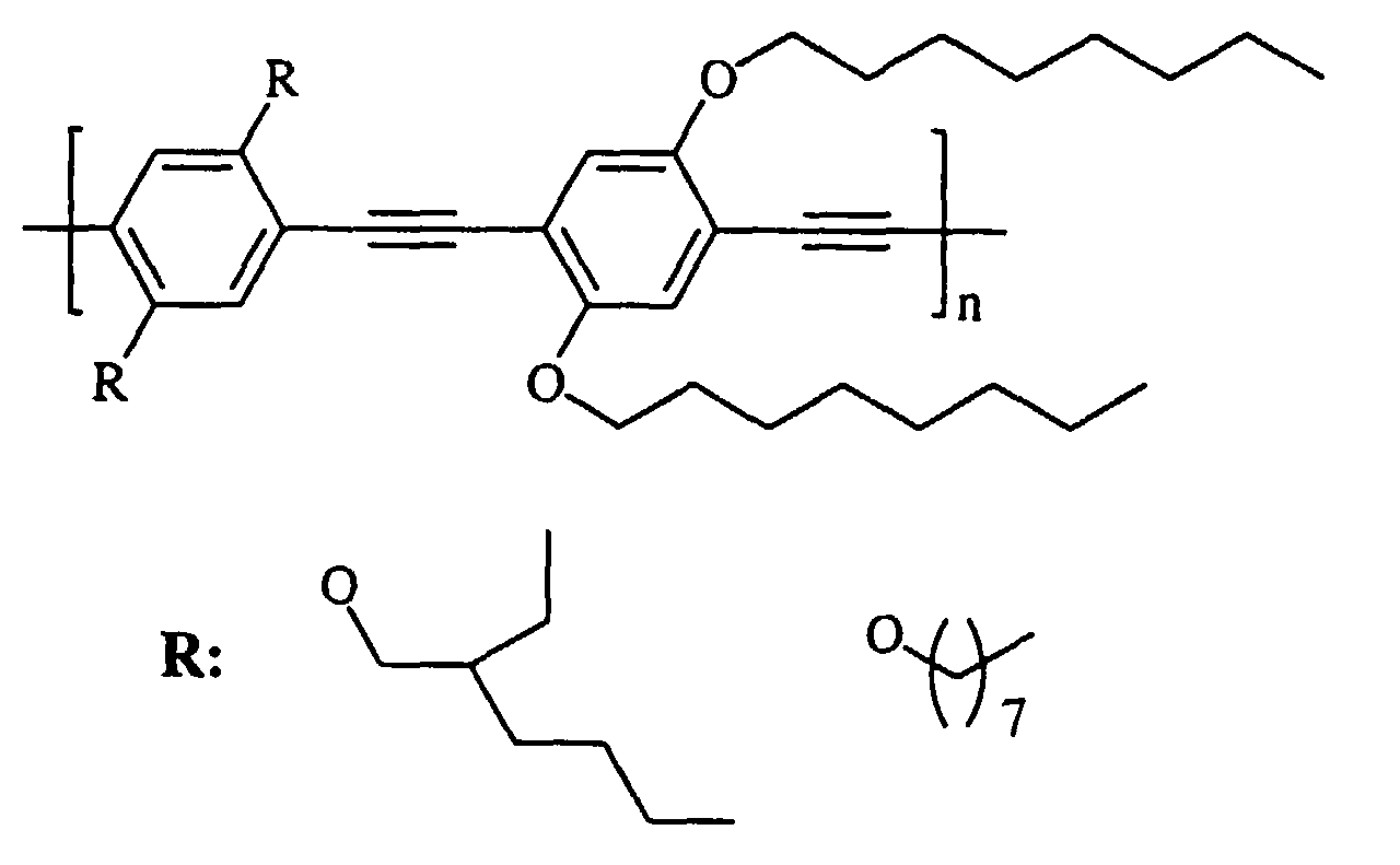 These substituted poly(phenyleneethynylene)s (PPEs) were
synthesized according to the procedures described in Ch. Weder et
al., Macromolecules, (1996) Vol. 29, p. 5157, and D. Steiger et al.,
Makromol. Chem. Phys., Rapid Comm., in press. The O-OPPE sample
had a number-average molecular weight, Mn, of 10,000 g mol-1, and
EHO-OPPE was of Mn = 84,000 g mol-1.
These substituted poly(phenyleneethynylene)s (PPEs) were
synthesized according to the procedures described in Ch. Weder et
al., Macromolecules, (1996) Vol. 29, p. 5157, and D. Steiger et al.,
Makromol. Chem. Phys., Rapid Comm., in press. The O-OPPE sample
had a number-average molecular weight, Mn, of 10,000 g mol-1, and
EHO-OPPE was of Mn = 84,000 g mol-1.
In addition, the polymer designated poly(1-methoxy-4-ethylhexyloxy-2,5-phenylenevinylene)
(MEH-PPV), synthesized according
to the procedure described in US Patent 5,204,038, was used. The
MEH-PPV was of a weight-average molecular weight Mw = 450,000 g
mol-1.
Thin blend photoluminescent layers with contents of 1 and 2
% w/w of PPE were prepared by casting a solution of the different
PPEs (5 or 10 mg) and ultra-high molecular weight polyethylene
(UHMW PE, Hostalen Gur 412. Hoechst AG) (0.5 g) in xylene (50 g)
(dissolution at 130 °C after degassing the mixture in vacuum at 25°C
for 15 min.) into a petri-dish of 11 cm in diameter. The resulting
gel layers were dried under ambient conditions for 24 h. These
unoriented blend layers had a homogeneous thickness of about 70
µm. The layers were drawn at temperatures of 90 - 120 °C on a
thermostatically controlled hot shoe to a series of different draw-ratios
(λ= final length/initial length) that ranged from 10 to 80.
Draw ratios were calculated from the displacement of distance marks
printed on the films prior to drawing. The oriented layers had a
thickness in the range from about 1 to about 10 µm.
In addition, thin blend layers with a content of 1% w/w of
MEH-PPV were prepared by casting a solution of the MEH-PPV and
ultra-high molecular weight polyethylene (UHMW PE, Hostalen Gur
412, Hoechst AG) in the identical manner as described above.
For reference purposes, also thick photoluminescent plates
with a content of 1 % w/w of PPE were produced by first casting a
solution of EHO-OPPE (20 mg) and high molecular weight
polyethylene (HMW-PE, Hostalen GR 7255, Hoechst AG, Mw of
∼400,000 g mol-1) (2 g) in xylene (200 g) (dissolution at 135 °C after
degassing the mixture in vacuum at 25°C for 15 min.) into a petri-dish
of 11 cm in diameter. The resulting gels were dried for 70 h at
ambient. Subsequently, the obtained blend was collected, placed
between two aluminium plates, fitted with 1 mm spacers, and melt-pressed
in a hot press for 5 min at temperatures of 140 - 150 °C
under a pressure of 3-5 metric tons to yield plates of a thickness of
approximately 1 mm. One plate was drawn at a temperature of 120
°C in an Instron tensile-tester equipped with a thermostatic
chamber, to yield an oriented plate of a draw-ratio of 3.6 and a
thickness of 1.5 mm.
The anisotropic photophysical behavior of these oriented layers
and plates was analyzed with polarized photoluminescence (PL) and
polarized UV/Vis absorption spectroscopy. For the photophysical
analysis, the polymer layers and plates were sandwiched between
two quartz slides; silicon oil fluid was applied in order to minimize
light scattering at the layer and plate surfaces. The dichroic ratios
were measured as defined above.
PL spectra were recorded on a SFEX Fluorolog 2 (Model F212
1), using unpolarized light (350 nm) for excitation and a Glan-Thomson
polarizer on the detector side.
UV/Vis absorption spectra were recorded on a Perkin Elmer
Lambda 900 instrument, fitted with motor driven Glan-Thomson
polarizers. Scattering effects were compensated in the absorption
measurements by subtracting the spectra of pure UHMW PE films of
comparable draw ratio and thickness.
Highly-polarized absorption and emission were observed for
the oriented layers, as visualized for emission in Figure 8 for a layer
containing 2 % w/w of EHO-PPE with a draw ratio of 80. The
polarized emission spectra of this particular layer show that this
layer is characterized by a dichroic ratio, measured in emission, of
72. The dichroic ratio of this particular layer, measured in
absorption, was 16. The influence of the draw ratio, the structure of
the side chains, and the composition of the blends on the dichroic
ratio measured in emission and absorption for PPEs are summarized
in Figures 9 and 10.
The 80 times drawn layer containing 1 % MEH-PPV displayed
a dichroic ratio, measured in emission, of 62.
By contrast, the oriented plate of a draw ratio of 3.6 and a
thickness of 1.5 mm was characterized by a dichroic ratio, measured
both in emission and absorption, of only about 2.
A display device was constructed according to the schematic of
Fig. 3 A. A UV lamp (Bioblock, VL-4LC, 4 Watts), operated at 365 nm,
was employed as a light source. Instead of the polarized PL layer (2),
an unoriented, thick polymer blend plate of 1 mm thickness of HMW
PE containing 1 % w/w of EHO-OPPE (prepared according to
Example A) was placed in between the UV source and a commercial
liquid crystal display, consisting of a patterned electrooptical light
valve (3) and one absorbing polarizer (2), arranged as shown in Fig 3
A. Selected patterns of the display device (segments) were switched
between the "on" and the "off" state, but the switching did not
change the appearance of the device. Due to the isotropic emission
from the unoriented plate, the entire area was illuminated by the
light source, and the device in both switching states showed a dim,
continuous, homogeneous yellow-green light.
This comparative example shows that employing a thick,
unoriented plate of photoluminescent material, characterized by a
dichroic ratio of unity in absorption and emission, in a device
configuration according to Fig. 3 A, does not yield a display device,
that can be switched between two different optical states ("bright"
and "dark").
Example B (Outside of the Invention) was repeated, but instead
of an unoriented, polymer blend plate of 1 mm thickness of HMW PE
containing 1 % w/w of EHO-OPPE, a 70 µm thin, unoriented layer of
UHMW PE containing 1 % w/w of EHO-OPPE (prepared according to
Example A) was used in the device. Selected patterns of the display
device (segments) were switched between the "on" and the "off"
state, but the switching did not change the appearance of the device.
Due to the isotropic emission from the unoriented layer, the entire
area was illuminated by the light source, and the device in both
switching states showed a continuous, homogeneous yellow-green
light.
This comparative example shows that employing a thin,
unoriented layer of photoluminescent material, characterized by a
dichroic ratio of unity in absorption and emission, in a device
configuration according to Fig. 3 A, does not yield a display device,
that can be switched between two different optical states ("bright"
and "dark").
Example B (Outside of the Invention) was repeated, but instead
of an unoriented, polymer blend plate of 1 mm thickness of HMW PE
containing 1 % w/w of EHO-OPPE, a 1.5 mm thick, oriented plate of
the same composition, of a draw-ratio of 3.6 and a dichroic ratio,
measured in emission and absorption, of about 2 (prepared according
to Example A) was used in the device. Selected patterns of the
display device (segments) were switched between the "on" and the
"off" state. The switching, indeed, led to a change in brightness, but
however, the contrast between the "on" and the "off" state, as
perceived by the human eye, was extremely low. One reason for the
poor contrast of this device is the fact that the switched segments in
their "off" state still exhibit a significant yellow-green emission.
This comparative example shows that employing a thick
photoluminescent plate with a moderate polarized absorption and
emission does not yield significantly improved characteristics of a
liquid crystal display.
Example B (Outside of the Invention) was repeated, but instead
of an unoriented, polymer blend plate of 1 mm thickness of HMW PE
containing 1 % w/w of EHO-OPPE, an oriented, about 30 µm thin
polymer blend layer of UHMW PE containing 1 % w/w of O-OPPE of a
draw ratio of about 5 and a dichroic ratio, measured in absorption, of
about 3.8 (prepared according to the methods described in Example
A), was used in the device. Selected patterns of the display device
(segments) were switched between the "on" and the "off" state. The
switching, indeed, led to a change in brightness, but however, the
contrast between the "on" and the "off" state, as perceived by the
human eye, was extremely low. One reason for the poor contrast of
this device is the fact that the switched segments in their "off" state
still exhibit a significant yellow-green emission.
This comparative example shows that employing a thin
photoluminescent layer with a moderate polarized absorption does
not yield significantly improved characteristics of a liquid crystal
display.
A display device was constructed according to the schematic of
Fig. 3 A. For convenience, a UV lamp (Bioblock, VL-4LC 4 Watts),
operated at 365 nm, was employed as a light source. (It should be
noted that the latter was not optimized for the particular absorption
band of the present photoluminescent materials). The polarized PL
layer (2), was a highly oriented, 2 µm thin polymer blend layer of
UHMW PE containing 2 % w/w of EHO-OPPE of a draw ratio of 80
and a dichroic ratio, measured in absorption, of 16, and, measured in
emission, of 72 (prepared according to Example A), and was placed
in between the UV source and a commercial liquid crystal display,
consisting of a patterned electrooptical light valve (3) and one
absorbing polarizer (2), arranged as shown in Fig 3 A. Selected
patterns of the display device (segments) were switched between the
"on" and the "off" state. The switching yielded a significant change
in brightness, that was perceived by the human eye as a change from
a very bright yellow-green to almost dark. In order to quantify the
observed outstanding contrast, the absolute brightness of the "on"
and the "off" state were measured with a Minolta LS 100 luminance
meter, which was fitted with a No 110 and a No 122 close-up lens.
The contrast ratio, which hereinafter is defined as the ratio between
the brightnesses of the "on" and "off" state, of the device was in
excess of 7. For the commercial direct-view LCD the contrast ratio
was about 3.5.
This example shows that employing a thin, polarized PL layer
characterized in a high degree of polarization for both, absorption
and emission, yields a liquid crystal display of dramatically improved
contrast.
Example 1 was repeated, but instead of the drawn blend film
containing 2 w/w % of EHO-OPPE in UHMW PE, an 80 times drawn
blend film containing 1 w/w % MEH-PPV in UHMW PE with a
dichroic ratio, measured in emission, of 62, prepared according to
Example A, was used. Selected patterns of the display device
(segments) were switched between the "on" and the "off" state. The
switching yielded a significant change in brightness, that was
perceived by the human eye as a change from a orange-red to almost
dark. The contrast and absolute brightness of the "on" and the "off"
state of the device were comparable to the device in Example 1.
This examples illustrates that by appropriately selecting the
photoluminescent material, devices of high brightness and high
contrast can be prepared that exhibit a different color.
A display device was constructed according to the schematic of
Fig. 5. For convenience, a UV lamp (Bioblock, VL-4LC, 4 Watts),
operated at 365 nm, was employed as a light source. (It should be
noted that the latter was not optimized for the particular absorption
bands of the present photoluminescent materials). The two polarized
PL layers (2, 12), were an oriented, 2 µm thin polymer blend layer of
UHMW PE containing 2 % w/w of EHO-OPPE of a draw ratio of 80
and a dichroic ratio, measured in absorption, of 16, and, measured in
emission, of 72 (2) and an oriented, 2 µm thin polymer blend layer of
UHMW PE containing 1% w/w MEH-PPV of a draw ratio of 80 and a
dichroic ratio, measured In absorption, of 14, and, measured in
emission, of 62 (12) (prepared according to Example A). The
polarized PL layers (2, 12) were placed with their orientation
directions perpendicular to one another and in between the UV
source and a commercial liquid crystal display, consisting of a
patterned electrooptical light valve (3) and one absorbing polarizer
(2), arranged as shown in Fig 5. Selected patterns of the display
device (segments) were switched between the "on" and the "off"
state. The switching, led to a significant change in color, that was
perceived by the human eye as a change from a bright yellow-green
to orange-red.
This examples illustrates that by appropriately selecting and
employing two polarized PL layers, display devices of high brightness
and high contrast can be prepared that exhibit two different colors
in the "on" and "off" state.
A commercial liquid crystalline mixture (K15, BDH Ltd.) was
placed onto the 80 times drawn blend films containing 2 % w/w of
EHO-PPE in UHMW PE and containing 1 % w/w MEH-PPV in
UHMW PE, respectively, prepared according to Example A were
used. The liquid crystalline material was found to immediately adopt
a uniaxial orientation.
This example shows that the layers according to the present
invention also can be placed inside a liquid crystal cell that operates
as a light valve in a display device, and functions not only as the
polarized PL layer but also as orientation layer (3d in Fig. 3 C) for the
liquid crystalline material.
Claims (20)
- An optoelectronic display device of high brightness and high contrast comprising at least one thin photoluminescent layer that is characterized in a high degree of polarization in its absorption and that is characterized in an emission which is either polarized or not, wherein said layer has a thickness of less than about 1 mm and a dichroic ratio of more than about 5.
- A display device according to claim 1 wherein said display device additionally comprises at least one electrooptical light valve.
- A display device according to claim 2 wherein said electrooptical light valve includes a liquid crystal cell having a liquid crystal layer which is electrically switchable between an operative state and inoperative state.
- A display device according to claims 1-3 wherein said device comprises at least one absorbing polarizer.
- A display device according to claims 1-4 wherein said photoluminescent layer is located between the viewer and the electrooptical light valve.
- A display device according to claims 1-5 wherein said device comprises two thin layers of material that are characterized in a high degree of polarization in their absorption, wherein said layers:i) have a thickness of less than about 1 mm and a dichroic ratio of more than 5;ii) have unequal photoemission or absorption spectra or both; andiii) have unequal absorption polarization directions.
- A display device according to claims 1-6, wherein said thin, polarized photoluminescent layer has a thickness of less than 300 µm.
- A display device according to claims 1-7, wherein said thin, polarized photoluminescent layer has a thickness of less than 50 µm.
- A display device according to claims 1-8, wherein said thin, polarized photoluminescent layer has a thickness of less than 10 µm.
- A display device according to claims 1-9, wherein said thin, polarized photoluminescent layer has a dichroic ratio of more than 10.
- A display device according to claims 1-10, wherein said thin, polarized photoluminescent layer has a dichroic ratio of more than 20.
- A display device according to claims 2-11, wherein said thin, polarized photoluminescent layer is located inside said electrooptical light valve.
- A display device according to claims 2-12, wherein said thin, polarized photoluminescent layer is located inside said electrooptical light valve and acts as orientation layer.
- A display device according to claims 1-13 wherein said thin, polarized photoluminescent layers are patterned.
- A display device according to claims 1-14 that is characterized in that said device comprises multiple polarized photoluminescent layer elements, pixels or arrays thereof.
- A display device according to claims 1-15 that is characterized in that said device additionally comprises multiple electrooptical light valves.
- A display device according to claims 1-16 that additionally comprises a light source wherein said light source is characterized in that it emission spectrum overlaps with the absorption spectrum of said photoluminescent layer.
- A display device according to claims 1-17 that additionally comprises at least one dichroic mirror.
- A display device according to claims 1-18 wherein said thin layer is made by a technique selected from the group consisting of tensile orientation, oriented growth, friction, photo-induced alignment and alignment in electric, magnetic and flow fields or combinations thereof, of photoluminescent substances.
- A display device according to claims 1-19 wherein said thin layer comprises a polymer.
Priority Applications (7)
| Application Number | Priority Date | Filing Date | Title |
|---|---|---|---|
| EP97111229A EP0889350A1 (en) | 1997-07-03 | 1997-07-03 | Photoluminescent display devices (I) |
| AU77843/98A AU7784398A (en) | 1997-07-03 | 1998-06-29 | Photoluminescent display devices and methods for making |
| JP50678799A JP2002508859A (en) | 1997-07-03 | 1998-06-29 | Photoluminescence display device and method of manufacturing the same |
| KR1019997012634A KR20010020612A (en) | 1997-07-03 | 1998-06-29 | Photoluminescent display devices and methods for making |
| PCT/IB1998/000998 WO1999001792A1 (en) | 1997-07-03 | 1998-06-29 | Photoluminescent display devices and methods for making |
| EP98925885A EP0991976A1 (en) | 1997-07-03 | 1998-06-29 | Photoluminescent display devices and methods for making |
| US09/476,358 US6891583B1 (en) | 1997-07-03 | 2000-01-03 | Photoluminescent display devices having a photoluminescent layer with a high degree of polarization in its absorption, and methods for making the same |
Applications Claiming Priority (1)
| Application Number | Priority Date | Filing Date | Title |
|---|---|---|---|
| EP97111229A EP0889350A1 (en) | 1997-07-03 | 1997-07-03 | Photoluminescent display devices (I) |
Publications (1)
| Publication Number | Publication Date |
|---|---|
| EP0889350A1 true EP0889350A1 (en) | 1999-01-07 |
Family
ID=8227009
Family Applications (2)
| Application Number | Title | Priority Date | Filing Date |
|---|---|---|---|
| EP97111229A Withdrawn EP0889350A1 (en) | 1997-07-03 | 1997-07-03 | Photoluminescent display devices (I) |
| EP98925885A Withdrawn EP0991976A1 (en) | 1997-07-03 | 1998-06-29 | Photoluminescent display devices and methods for making |
Family Applications After (1)
| Application Number | Title | Priority Date | Filing Date |
|---|---|---|---|
| EP98925885A Withdrawn EP0991976A1 (en) | 1997-07-03 | 1998-06-29 | Photoluminescent display devices and methods for making |
Country Status (5)
| Country | Link |
|---|---|
| EP (2) | EP0889350A1 (en) |
| JP (1) | JP2002508859A (en) |
| KR (1) | KR20010020612A (en) |
| AU (1) | AU7784398A (en) |
| WO (1) | WO1999001792A1 (en) |
Cited By (103)
| Publication number | Priority date | Publication date | Assignee | Title |
|---|---|---|---|---|
| US6645401B2 (en) | 2001-08-17 | 2003-11-11 | Merck Patent Gmbh | Conjugated copolymers of dithienothiophene with vinylene or acetylene |
| US6676857B2 (en) | 2001-07-25 | 2004-01-13 | Merck Patent Gesellschaft Mit | Mono-, oligo- and poly-4-fluorothiophenes and their use as charge transport materials |
| US6695978B2 (en) | 2001-09-29 | 2004-02-24 | Merck Patent Gesellschaft Mit Beschraenkter Haftung | Mono-, oligo- and polymers of benzo[b]thiophene and 2,2′-bisbenzo[b]thiophene and their use as charge transport materials |
| WO2003085608A3 (en) * | 2002-04-04 | 2004-02-26 | Landqart | Device for verifying security features |
| WO2003085609A3 (en) * | 2002-04-04 | 2004-02-26 | Landqart | Device for checking security elements |
| US6806374B2 (en) | 2001-07-25 | 2004-10-19 | Merck Patent Gmbh | Mono-, oligo- and poly-3-(1,1-difluoroalkyl)thiophenes and their use as charge transport materials |
| US6805922B2 (en) | 2001-08-17 | 2004-10-19 | Merck Patent Gmbh | Mono-, oligo-and polyalkylidenefluorenes and their use as charge transport materials |
| US6824706B2 (en) | 2001-07-25 | 2004-11-30 | Merck Patent Gesellschaft Mit Beschrank Haftung | Mono-, Oligo- and poly-difluorovinyl-(hetero)arylenes, their synthesis and their use as charge transport materials |
| EP1136871A3 (en) * | 2000-03-14 | 2004-12-01 | Philips Intellectual Property & Standards GmbH | Colour liquid crystal display device |
| US6863841B2 (en) | 2001-12-13 | 2005-03-08 | Merck Patent Gmbh | Oxadiazole derivative and its use as charge transport and light emitting material |
| US6913710B2 (en) | 2002-04-24 | 2005-07-05 | Merck Patent Gmbh | Reactive mesogenic benzodithiophenes |
| EP1754736A1 (en) | 2005-08-16 | 2007-02-21 | Merck Patent GmbH | Process for the polymerisation of thiophene or selenophene derivatives |
| US7294288B2 (en) | 2003-08-06 | 2007-11-13 | Merck Patent Gesellschaft Mit Beschrankter Haftung | Process of preparing regioregular polymers |
| DE112006002830T5 (en) | 2005-11-24 | 2008-09-25 | Merck Patent Gmbh | Process for the preparation of regioregular polymers |
| DE112006002690T5 (en) | 2005-11-24 | 2008-10-23 | Merck Patent Gmbh | Regioregular polyselenophene |
| WO2010028728A1 (en) * | 2008-09-10 | 2010-03-18 | Merck Patent Gmbh | Liquid crystal display with a fluorescent backlight emitting polarised light |
| WO2011018144A2 (en) | 2009-08-12 | 2011-02-17 | Merck Patent Gmbh | Phenanthro[1,10,9,8-c,d,e,f,g]carbazole polymers and their use as organic semiconductors |
| DE112009001505T5 (en) | 2008-08-18 | 2011-07-14 | Merck Patent GmbH, 64293 | Indacenodithiophene and indacenodiselenophene polymers and their use as organic semiconductors |
| DE112009001782T5 (en) | 2008-09-19 | 2011-07-28 | Merck Patent GmbH, 64293 | Bis (thienocyclopenta) benzothiadiazole-derived polymers and their use as organic semiconductors |
| DE112009001784T5 (en) | 2008-09-19 | 2011-07-28 | Merck Patent GmbH, 64293 | Benzo-bis (silo-thiophene) derived polymers and their use as organic semiconductors |
| WO2011098113A2 (en) | 2010-02-15 | 2011-08-18 | Merck Patent Gmbh | Semiconducting polymers |
| WO2011116866A1 (en) | 2010-03-24 | 2011-09-29 | Merck Patent Gmbh | Polymers of 8,9-dihydrobenzo[def]carbazole and their use as organic semiconductors |
| WO2011131280A1 (en) | 2010-04-19 | 2011-10-27 | Merck Patent Gmbh | Polymers of benzodithiophene and their use as organic semiconductors |
| WO2012003919A2 (en) | 2010-07-08 | 2012-01-12 | Merck Patent Gmbh | Semiconducting polymers |
| WO2012019683A2 (en) | 2010-08-13 | 2012-02-16 | Merck Patent Gmbh | Anthra[2,3-b:7,6-b']dithiophene derivatives and their use as organic semiconductors |
| WO2012028246A1 (en) | 2010-09-04 | 2012-03-08 | Merck Patent Gmbh | Conjugated polymers |
| WO2012031659A1 (en) | 2010-09-10 | 2012-03-15 | Merck Patent Gmbh | Anthra[2,3-b:7,6b']dithiophene derivatives and their use as organic semiconductors |
| WO2012052099A1 (en) | 2010-10-20 | 2012-04-26 | Merck Patent Gmbh | Conjugated polymers |
| WO2012076092A1 (en) | 2010-12-06 | 2012-06-14 | Merck Patent Gmbh | Non-linear acene derivatives and their use as organic semiconductors |
| WO2012079675A2 (en) | 2010-12-17 | 2012-06-21 | Merck Patent Gmbh | Conjugated polymers |
| WO2012100900A1 (en) | 2011-01-28 | 2012-08-02 | Merck Patent Gmbh | Flavanthrene derivatives and their use as organic semiconductors |
| WO2012123058A1 (en) | 2011-03-11 | 2012-09-20 | Merck Patent Gmbh | Dinaphtho[2,3-a:2',3'-h]phenazines and their use as organic semiconductors |
| WO2012123060A1 (en) | 2011-03-11 | 2012-09-20 | Merck Patent Gmbh | Conjugated polymers |
| WO2012130365A1 (en) | 2011-03-25 | 2012-10-04 | Merck Patent Gmbh | Pyrrolo[3,2-b]pyrrole-2,5-diones and their use as organic semiconductors |
| WO2012143081A1 (en) | 2011-04-18 | 2012-10-26 | Merck Patent Gmbh | Conjugated polymers |
| WO2012156022A1 (en) | 2011-05-16 | 2012-11-22 | Merck Patent Gmbh | Conjugated polymers |
| WO2013000532A1 (en) | 2011-06-28 | 2013-01-03 | Merck Patent Gmbh | Indaceno derivatives as organic semiconductors |
| WO2013007334A2 (en) | 2011-07-08 | 2013-01-17 | Merck Patent Gmbh | Conjugated polymers |
| WO2013010614A2 (en) | 2011-07-19 | 2013-01-24 | Merck Patent Gmbh | Organic semiconductors |
| WO2013010615A1 (en) | 2011-07-21 | 2013-01-24 | Merck Patent Gmbh | Conjugated polymers |
| WO2013013765A1 (en) | 2011-07-27 | 2013-01-31 | Merck Patent Gmbh | Small molecules and their use as organic semiconductors |
| WO2013045014A1 (en) | 2011-09-28 | 2013-04-04 | Merck Patent Gmbh | Conjugated polymers |
| WO2013056775A1 (en) | 2011-10-20 | 2013-04-25 | Merck Patent Gmbh | Organic semiconductors |
| DE112011102301T5 (en) | 2010-07-09 | 2013-05-16 | Merck Patent Gmbh | Semiconducting polymers |
| US8501902B2 (en) | 2005-08-16 | 2013-08-06 | Merck Patent Gmbh | Process for the polymerisation of thiophene or selenophene compounds |
| WO2013120575A1 (en) | 2012-02-16 | 2013-08-22 | Merck Patent Gmbh | Organic semiconducting polymers |
| WO2013120590A1 (en) | 2012-02-15 | 2013-08-22 | Merck Patent Gmbh | Conjugated polymers |
| WO2013120591A2 (en) | 2012-02-15 | 2013-08-22 | Merck Patent Gmbh | Conjugated polymers |
| WO2013135339A2 (en) | 2012-03-16 | 2013-09-19 | Merck Patent Gmbh | Conjugated polymers |
| WO2013159863A1 (en) | 2012-04-25 | 2013-10-31 | Merck Patent Gmbh | Conjugated polymers |
| WO2013159862A1 (en) | 2012-04-25 | 2013-10-31 | Merck Patent Gmbh | Conjugated polymers |
| WO2013182262A1 (en) | 2012-06-04 | 2013-12-12 | Merck Patent Gmbh | Organic semiconductors |
| WO2013182264A1 (en) | 2012-06-05 | 2013-12-12 | Merck Patent Gmbh | Small molecules and their use as organic semiconductors |
| WO2014005667A1 (en) | 2012-07-02 | 2014-01-09 | Merck Patent Gmbh | Conjugated polymers |
| WO2014029453A1 (en) | 2012-08-24 | 2014-02-27 | Merck Patent Gmbh | Conjugated polymers |
| WO2014086457A1 (en) | 2012-12-07 | 2014-06-12 | Merck Patent Gmbh | Polymer comprising a naphthalene group and its use in organic electronic devices |
| WO2014094955A1 (en) | 2012-12-18 | 2014-06-26 | Merck Patent Gmbh | Polymer comprising a thiadiazol group, the production of such polymer and its use in organic electronic devices |
| WO2014202184A1 (en) | 2013-06-21 | 2014-12-24 | Merck Patent Gmbh | Conjugated polymers |
| WO2015036075A1 (en) | 2013-09-11 | 2015-03-19 | Merck Patent Gmbh | Cyclohexadiene fullerene derivatives |
| WO2015043722A1 (en) | 2013-09-30 | 2015-04-02 | Merck Patent Gmbh | Azaborinine derivatives, their synthesis and use in organic electronic devices |
| WO2015058827A1 (en) | 2013-10-22 | 2015-04-30 | Merck Patent Gmbh | Conjugated polymers |
| WO2015067336A2 (en) | 2013-11-06 | 2015-05-14 | Merck Patent Gmbh | Conjugated polymers |
| WO2015078551A1 (en) | 2013-11-28 | 2015-06-04 | Merck Patent Gmbh | Novel polycyclic polymer comprising thiophene units, a method of producing and uses of such polymer |
| WO2015139802A1 (en) | 2014-03-17 | 2015-09-24 | Merck Patent Gmbh | Organic semiconducting compounds |
| WO2015149905A1 (en) | 2014-03-31 | 2015-10-08 | Merck Patent Gmbh | Fused bis-aryl fullerene derivatives |
| WO2015192942A1 (en) | 2014-06-17 | 2015-12-23 | Merck Patent Gmbh | Fullerene derivatives |
| WO2016015804A1 (en) | 2014-07-29 | 2016-02-04 | Merck Patent Gmbh | Tetra-heteroaryl indacenodithiophene-based polycyclic polymers and their use |
| EP3070756A1 (en) | 2015-03-18 | 2016-09-21 | Merck Patent GmbH | Semiconductor mixtures comprising nanoparticles |
| WO2016180515A1 (en) | 2015-05-12 | 2016-11-17 | Merck Patent Gmbh | Thiadiazolopyridine polymers, their synthesis and their use |
| WO2017020988A1 (en) | 2015-08-06 | 2017-02-09 | Merck Patent Gmbh | Organic semiconductor compositions and their use in the production of organic electronic devices |
| EP3151297A1 (en) | 2015-09-30 | 2017-04-05 | InnovationLab GmbH | Conjugated polymers with thermally splittable oxalate side groups |
| WO2017157782A1 (en) | 2016-03-15 | 2017-09-21 | Merck Patent Gmbh | Organic semiconductors |
| WO2017157504A1 (en) | 2016-03-15 | 2017-09-21 | Merck Patent Gmbh | Organic semiconductors |
| WO2018007479A1 (en) | 2016-07-08 | 2018-01-11 | Merck Patent Gmbh | Organic semiconducting compounds |
| WO2018007431A1 (en) | 2016-07-08 | 2018-01-11 | Merck Patent Gmbh | Fused dithienothiophene derivatives and their use as organic semiconductors |
| WO2018029159A1 (en) | 2016-08-11 | 2018-02-15 | Merck Patent Gmbh | Organic semiconducting compounds comprising a tetraazapyrene core |
| WO2018036914A1 (en) | 2016-08-22 | 2018-03-01 | Merck Patent Gmbh | Organic semiconducting compounds |
| WO2018041768A1 (en) | 2016-08-29 | 2018-03-08 | Merck Patent Gmbh | 1,3-dithiolo[5,6-f]benzo-2,1,3-thiadiazole or 1,3-dithiolo[6,7-g]quinoxaline based organic semiconductors |
| EP3306690A1 (en) | 2016-10-05 | 2018-04-11 | Merck Patent GmbH | Organic semiconducting compounds |
| WO2018065356A1 (en) | 2016-10-05 | 2018-04-12 | Merck Patent Gmbh | Organic semiconducting compounds |
| WO2018065350A1 (en) | 2016-10-05 | 2018-04-12 | Merck Patent Gmbh | Organic semiconducting compounds |
| WO2018078080A1 (en) | 2016-10-31 | 2018-05-03 | Merck Patent Gmbh | Organic semiconducting compounds |
| EP3333170A1 (en) | 2016-12-06 | 2018-06-13 | Merck Patent GmbH | Asymmetrical polycyclic compounds for use in organic semiconductors |
| WO2018162447A1 (en) | 2017-03-09 | 2018-09-13 | Merck Patent Gmbh | Organic semiconducting compounds |
| WO2019030382A1 (en) | 2017-08-11 | 2019-02-14 | Merck Patent Gmbh | Organic semiconducting polymer |
| WO2019052935A1 (en) | 2017-09-13 | 2019-03-21 | Merck Patent Gmbh | Organic semiconducting compounds |
| WO2019086400A1 (en) | 2017-11-02 | 2019-05-09 | Merck Patent Gmbh | Organic semiconducting compounds |
| WO2019091995A1 (en) | 2017-11-10 | 2019-05-16 | Merck Patent Gmbh | Organic semiconducting compounds |
| WO2019154973A1 (en) | 2018-02-12 | 2019-08-15 | Merck Patent Gmbh | Organic semiconducting compounds |
| WO2019185578A1 (en) | 2018-03-28 | 2019-10-03 | Merck Patent Gmbh | Organic semiconducting compounds |
| WO2019185580A1 (en) | 2018-03-28 | 2019-10-03 | Merck Patent Gmbh | Organic semiconducting compounds |
| WO2019206926A1 (en) | 2018-04-27 | 2019-10-31 | Merck Patent Gmbh | Organic semiconducting polymers |
| WO2020011831A1 (en) | 2018-07-13 | 2020-01-16 | Merck Patent Gmbh | Organic semiconducting compounds |
| WO2020048939A1 (en) | 2018-09-06 | 2020-03-12 | Merck Patent Gmbh | Organic semiconducting compounds |
| US10636974B2 (en) | 2014-04-24 | 2020-04-28 | The Trustees Of Columbia University In The City Of New York | Molecular compositions, materials, and methods for efficient multiple exciton generation |
| WO2020161052A1 (en) | 2019-02-06 | 2020-08-13 | Merck Patent Gmbh | Organic semiconducting polymers |
| WO2020178298A1 (en) | 2019-03-07 | 2020-09-10 | Raynergy Tek Inc. | Organic semiconducting composition |
| WO2020187867A1 (en) | 2019-03-19 | 2020-09-24 | Raynergy Tek Inc. | Organic semiconductors |
| FR3097685A1 (en) | 2019-06-24 | 2020-12-25 | Isorg | A formulation comprising a p-type organic semiconductor material and an n-type semiconductor material |
| FR3097686A1 (en) | 2019-06-24 | 2020-12-25 | Isorg | A formulation comprising a p-type organic semiconductor material and an n-type semiconductor material |
| FR3097684A1 (en) | 2019-06-24 | 2020-12-25 | Isorg | A formulation comprising a p-type organic semiconductor material and an n-type semiconductor material |
| FR3097687A1 (en) | 2019-06-24 | 2020-12-25 | Isorg | A formulation comprising a p-type organic semiconductor material and an n-type semiconductor material |
| US11930694B2 (en) | 2020-06-08 | 2024-03-12 | University Of Waterloo | Polymer semiconductors containing acrylyl or acrylyl-like side chain and their devices |
Families Citing this family (3)
| Publication number | Priority date | Publication date | Assignee | Title |
|---|---|---|---|---|
| DE60027754T2 (en) * | 1999-07-22 | 2007-05-03 | Landqart | PROCESS FOR PREPARING PHOTOLUMINESCENT POLARIZERS |
| KR100516296B1 (en) | 2003-01-21 | 2005-09-21 | 주식회사 팬택앤큐리텔 | Usb interface device by using function of switch |
| US7557876B2 (en) * | 2003-07-25 | 2009-07-07 | Nitto Denko Corporation | Anisotropic fluorescent thin crystal film and backlight system and liquid crystal display incorporating the same |
Citations (2)
| Publication number | Priority date | Publication date | Assignee | Title |
|---|---|---|---|---|
| DE2640909A1 (en) * | 1976-09-10 | 1978-03-23 | Siemens Ag | Passive light amplification in electro-optic display - uses filter plate located behind fluorescent plate for ambient light amplification (SW 27.6.77) |
| US4142781A (en) * | 1975-12-03 | 1979-03-06 | Siemens Aktiengesellschaft | Electro-optical display device with electro-optical light valves |
-
1997
- 1997-07-03 EP EP97111229A patent/EP0889350A1/en not_active Withdrawn
-
1998
- 1998-06-29 JP JP50678799A patent/JP2002508859A/en active Pending
- 1998-06-29 WO PCT/IB1998/000998 patent/WO1999001792A1/en not_active Ceased
- 1998-06-29 AU AU77843/98A patent/AU7784398A/en not_active Abandoned
- 1998-06-29 EP EP98925885A patent/EP0991976A1/en not_active Withdrawn
- 1998-06-29 KR KR1019997012634A patent/KR20010020612A/en not_active Withdrawn
Patent Citations (2)
| Publication number | Priority date | Publication date | Assignee | Title |
|---|---|---|---|---|
| US4142781A (en) * | 1975-12-03 | 1979-03-06 | Siemens Aktiengesellschaft | Electro-optical display device with electro-optical light valves |
| DE2640909A1 (en) * | 1976-09-10 | 1978-03-23 | Siemens Ag | Passive light amplification in electro-optic display - uses filter plate located behind fluorescent plate for ambient light amplification (SW 27.6.77) |
Cited By (119)
| Publication number | Priority date | Publication date | Assignee | Title |
|---|---|---|---|---|
| EP1136871A3 (en) * | 2000-03-14 | 2004-12-01 | Philips Intellectual Property & Standards GmbH | Colour liquid crystal display device |
| US6676857B2 (en) | 2001-07-25 | 2004-01-13 | Merck Patent Gesellschaft Mit | Mono-, oligo- and poly-4-fluorothiophenes and their use as charge transport materials |
| US6806374B2 (en) | 2001-07-25 | 2004-10-19 | Merck Patent Gmbh | Mono-, oligo- and poly-3-(1,1-difluoroalkyl)thiophenes and their use as charge transport materials |
| US6824706B2 (en) | 2001-07-25 | 2004-11-30 | Merck Patent Gesellschaft Mit Beschrank Haftung | Mono-, Oligo- and poly-difluorovinyl-(hetero)arylenes, their synthesis and their use as charge transport materials |
| US6645401B2 (en) | 2001-08-17 | 2003-11-11 | Merck Patent Gmbh | Conjugated copolymers of dithienothiophene with vinylene or acetylene |
| US6805922B2 (en) | 2001-08-17 | 2004-10-19 | Merck Patent Gmbh | Mono-, oligo-and polyalkylidenefluorenes and their use as charge transport materials |
| US6695978B2 (en) | 2001-09-29 | 2004-02-24 | Merck Patent Gesellschaft Mit Beschraenkter Haftung | Mono-, oligo- and polymers of benzo[b]thiophene and 2,2′-bisbenzo[b]thiophene and their use as charge transport materials |
| US6863841B2 (en) | 2001-12-13 | 2005-03-08 | Merck Patent Gmbh | Oxadiazole derivative and its use as charge transport and light emitting material |
| WO2003085608A3 (en) * | 2002-04-04 | 2004-02-26 | Landqart | Device for verifying security features |
| WO2003085609A3 (en) * | 2002-04-04 | 2004-02-26 | Landqart | Device for checking security elements |
| US6913710B2 (en) | 2002-04-24 | 2005-07-05 | Merck Patent Gmbh | Reactive mesogenic benzodithiophenes |
| US7294288B2 (en) | 2003-08-06 | 2007-11-13 | Merck Patent Gesellschaft Mit Beschrankter Haftung | Process of preparing regioregular polymers |
| EP1754736A1 (en) | 2005-08-16 | 2007-02-21 | Merck Patent GmbH | Process for the polymerisation of thiophene or selenophene derivatives |
| US8501902B2 (en) | 2005-08-16 | 2013-08-06 | Merck Patent Gmbh | Process for the polymerisation of thiophene or selenophene compounds |
| DE112006002830T5 (en) | 2005-11-24 | 2008-09-25 | Merck Patent Gmbh | Process for the preparation of regioregular polymers |
| DE112006002690T5 (en) | 2005-11-24 | 2008-10-23 | Merck Patent Gmbh | Regioregular polyselenophene |
| DE112009001505T5 (en) | 2008-08-18 | 2011-07-14 | Merck Patent GmbH, 64293 | Indacenodithiophene and indacenodiselenophene polymers and their use as organic semiconductors |
| US8879024B2 (en) | 2008-09-10 | 2014-11-04 | Merck Patent Gmbh | Liquid crystal display with a fluorescent backlight emitting polarised light |
| GB2475464B (en) * | 2008-09-10 | 2013-01-02 | Merck Patent Gmbh | Liquid crystal display with a fluorescent backlight emitting polarised light |
| GB2475464A (en) * | 2008-09-10 | 2011-05-18 | Merck Patent Gmbh | Liquid crystal display with a fluorescent backlight emitting polarised light |
| WO2010028728A1 (en) * | 2008-09-10 | 2010-03-18 | Merck Patent Gmbh | Liquid crystal display with a fluorescent backlight emitting polarised light |
| DE112009001782T5 (en) | 2008-09-19 | 2011-07-28 | Merck Patent GmbH, 64293 | Bis (thienocyclopenta) benzothiadiazole-derived polymers and their use as organic semiconductors |
| DE112009001784T5 (en) | 2008-09-19 | 2011-07-28 | Merck Patent GmbH, 64293 | Benzo-bis (silo-thiophene) derived polymers and their use as organic semiconductors |
| WO2011018144A2 (en) | 2009-08-12 | 2011-02-17 | Merck Patent Gmbh | Phenanthro[1,10,9,8-c,d,e,f,g]carbazole polymers and their use as organic semiconductors |
| WO2011098113A2 (en) | 2010-02-15 | 2011-08-18 | Merck Patent Gmbh | Semiconducting polymers |
| EP2631230A1 (en) | 2010-02-15 | 2013-08-28 | Merck Patent GmbH | Semiconducting Polymers |
| WO2011116866A1 (en) | 2010-03-24 | 2011-09-29 | Merck Patent Gmbh | Polymers of 8,9-dihydrobenzo[def]carbazole and their use as organic semiconductors |
| EP3243818A1 (en) | 2010-04-19 | 2017-11-15 | Merck Patent GmbH | Polymers of benzodithiophene and their use as organic semiconductors |
| WO2011131280A1 (en) | 2010-04-19 | 2011-10-27 | Merck Patent Gmbh | Polymers of benzodithiophene and their use as organic semiconductors |
| DE112011101363T5 (en) | 2010-04-19 | 2013-02-07 | Merck Patent Gmbh | Polymers of benzodithiophene and their use as organic semiconductors |
| WO2012003919A2 (en) | 2010-07-08 | 2012-01-12 | Merck Patent Gmbh | Semiconducting polymers |
| DE112011102301T5 (en) | 2010-07-09 | 2013-05-16 | Merck Patent Gmbh | Semiconducting polymers |
| WO2012019683A2 (en) | 2010-08-13 | 2012-02-16 | Merck Patent Gmbh | Anthra[2,3-b:7,6-b']dithiophene derivatives and their use as organic semiconductors |
| WO2012028246A1 (en) | 2010-09-04 | 2012-03-08 | Merck Patent Gmbh | Conjugated polymers |
| DE112011102915T5 (en) | 2010-09-04 | 2013-07-11 | Merck Patent Gmbh | Conjugated polymers |
| WO2012031659A1 (en) | 2010-09-10 | 2012-03-15 | Merck Patent Gmbh | Anthra[2,3-b:7,6b']dithiophene derivatives and their use as organic semiconductors |
| WO2012052099A1 (en) | 2010-10-20 | 2012-04-26 | Merck Patent Gmbh | Conjugated polymers |
| DE112011103524T5 (en) | 2010-10-20 | 2013-10-17 | Merck Patent Gmbh | Conjugated polymers |
| WO2012076092A1 (en) | 2010-12-06 | 2012-06-14 | Merck Patent Gmbh | Non-linear acene derivatives and their use as organic semiconductors |
| WO2012079675A2 (en) | 2010-12-17 | 2012-06-21 | Merck Patent Gmbh | Conjugated polymers |
| DE112011104436T5 (en) | 2010-12-17 | 2013-09-12 | Merck Patent Gmbh | Conjugated polymers |
| WO2012100900A1 (en) | 2011-01-28 | 2012-08-02 | Merck Patent Gmbh | Flavanthrene derivatives and their use as organic semiconductors |
| WO2012123060A1 (en) | 2011-03-11 | 2012-09-20 | Merck Patent Gmbh | Conjugated polymers |
| WO2012123058A1 (en) | 2011-03-11 | 2012-09-20 | Merck Patent Gmbh | Dinaphtho[2,3-a:2',3'-h]phenazines and their use as organic semiconductors |
| WO2012130365A1 (en) | 2011-03-25 | 2012-10-04 | Merck Patent Gmbh | Pyrrolo[3,2-b]pyrrole-2,5-diones and their use as organic semiconductors |
| WO2012143081A1 (en) | 2011-04-18 | 2012-10-26 | Merck Patent Gmbh | Conjugated polymers |
| WO2012156022A1 (en) | 2011-05-16 | 2012-11-22 | Merck Patent Gmbh | Conjugated polymers |
| WO2013000532A1 (en) | 2011-06-28 | 2013-01-03 | Merck Patent Gmbh | Indaceno derivatives as organic semiconductors |
| WO2013007334A2 (en) | 2011-07-08 | 2013-01-17 | Merck Patent Gmbh | Conjugated polymers |
| WO2013010614A2 (en) | 2011-07-19 | 2013-01-24 | Merck Patent Gmbh | Organic semiconductors |
| WO2013010615A1 (en) | 2011-07-21 | 2013-01-24 | Merck Patent Gmbh | Conjugated polymers |
| WO2013013765A1 (en) | 2011-07-27 | 2013-01-31 | Merck Patent Gmbh | Small molecules and their use as organic semiconductors |
| WO2013045014A1 (en) | 2011-09-28 | 2013-04-04 | Merck Patent Gmbh | Conjugated polymers |
| WO2013056775A1 (en) | 2011-10-20 | 2013-04-25 | Merck Patent Gmbh | Organic semiconductors |
| WO2013120591A2 (en) | 2012-02-15 | 2013-08-22 | Merck Patent Gmbh | Conjugated polymers |
| WO2013120590A1 (en) | 2012-02-15 | 2013-08-22 | Merck Patent Gmbh | Conjugated polymers |
| US9178166B2 (en) | 2012-02-15 | 2015-11-03 | Merck Patent Gmbh | Conjugated polymers |
| WO2013120575A1 (en) | 2012-02-16 | 2013-08-22 | Merck Patent Gmbh | Organic semiconducting polymers |
| WO2013135339A2 (en) | 2012-03-16 | 2013-09-19 | Merck Patent Gmbh | Conjugated polymers |
| WO2013159863A1 (en) | 2012-04-25 | 2013-10-31 | Merck Patent Gmbh | Conjugated polymers |
| WO2013159862A1 (en) | 2012-04-25 | 2013-10-31 | Merck Patent Gmbh | Conjugated polymers |
| WO2013182262A1 (en) | 2012-06-04 | 2013-12-12 | Merck Patent Gmbh | Organic semiconductors |
| WO2013182264A1 (en) | 2012-06-05 | 2013-12-12 | Merck Patent Gmbh | Small molecules and their use as organic semiconductors |
| WO2014005667A1 (en) | 2012-07-02 | 2014-01-09 | Merck Patent Gmbh | Conjugated polymers |
| WO2014029453A1 (en) | 2012-08-24 | 2014-02-27 | Merck Patent Gmbh | Conjugated polymers |
| WO2014086457A1 (en) | 2012-12-07 | 2014-06-12 | Merck Patent Gmbh | Polymer comprising a naphthalene group and its use in organic electronic devices |
| WO2014094955A1 (en) | 2012-12-18 | 2014-06-26 | Merck Patent Gmbh | Polymer comprising a thiadiazol group, the production of such polymer and its use in organic electronic devices |
| WO2014202184A1 (en) | 2013-06-21 | 2014-12-24 | Merck Patent Gmbh | Conjugated polymers |
| WO2015036075A1 (en) | 2013-09-11 | 2015-03-19 | Merck Patent Gmbh | Cyclohexadiene fullerene derivatives |
| WO2015043722A1 (en) | 2013-09-30 | 2015-04-02 | Merck Patent Gmbh | Azaborinine derivatives, their synthesis and use in organic electronic devices |
| WO2015058827A1 (en) | 2013-10-22 | 2015-04-30 | Merck Patent Gmbh | Conjugated polymers |
| WO2015067336A2 (en) | 2013-11-06 | 2015-05-14 | Merck Patent Gmbh | Conjugated polymers |
| WO2015078551A1 (en) | 2013-11-28 | 2015-06-04 | Merck Patent Gmbh | Novel polycyclic polymer comprising thiophene units, a method of producing and uses of such polymer |
| WO2015139802A1 (en) | 2014-03-17 | 2015-09-24 | Merck Patent Gmbh | Organic semiconducting compounds |
| WO2015149905A1 (en) | 2014-03-31 | 2015-10-08 | Merck Patent Gmbh | Fused bis-aryl fullerene derivatives |
| US10636974B2 (en) | 2014-04-24 | 2020-04-28 | The Trustees Of Columbia University In The City Of New York | Molecular compositions, materials, and methods for efficient multiple exciton generation |
| WO2015192942A1 (en) | 2014-06-17 | 2015-12-23 | Merck Patent Gmbh | Fullerene derivatives |
| EP4008708A1 (en) | 2014-06-17 | 2022-06-08 | Nano-C, Inc. | Fullerene derivatives for organic semiconductors |
| WO2016015804A1 (en) | 2014-07-29 | 2016-02-04 | Merck Patent Gmbh | Tetra-heteroaryl indacenodithiophene-based polycyclic polymers and their use |
| EP3070756A1 (en) | 2015-03-18 | 2016-09-21 | Merck Patent GmbH | Semiconductor mixtures comprising nanoparticles |
| WO2016180515A1 (en) | 2015-05-12 | 2016-11-17 | Merck Patent Gmbh | Thiadiazolopyridine polymers, their synthesis and their use |
| WO2017020988A1 (en) | 2015-08-06 | 2017-02-09 | Merck Patent Gmbh | Organic semiconductor compositions and their use in the production of organic electronic devices |
| EP3151297A1 (en) | 2015-09-30 | 2017-04-05 | InnovationLab GmbH | Conjugated polymers with thermally splittable oxalate side groups |
| WO2017157782A1 (en) | 2016-03-15 | 2017-09-21 | Merck Patent Gmbh | Organic semiconductors |
| WO2017157504A1 (en) | 2016-03-15 | 2017-09-21 | Merck Patent Gmbh | Organic semiconductors |
| WO2018007479A1 (en) | 2016-07-08 | 2018-01-11 | Merck Patent Gmbh | Organic semiconducting compounds |
| WO2018007431A1 (en) | 2016-07-08 | 2018-01-11 | Merck Patent Gmbh | Fused dithienothiophene derivatives and their use as organic semiconductors |
| WO2018029159A1 (en) | 2016-08-11 | 2018-02-15 | Merck Patent Gmbh | Organic semiconducting compounds comprising a tetraazapyrene core |
| DE112017003977T5 (en) | 2016-08-11 | 2019-07-04 | Merck Patent Gmbh | ORGANIC SEMICONDUCTOR COMPOUNDS COMPRISING A TETRAAZAPYRENE CORE |
| WO2018036914A1 (en) | 2016-08-22 | 2018-03-01 | Merck Patent Gmbh | Organic semiconducting compounds |
| WO2018041768A1 (en) | 2016-08-29 | 2018-03-08 | Merck Patent Gmbh | 1,3-dithiolo[5,6-f]benzo-2,1,3-thiadiazole or 1,3-dithiolo[6,7-g]quinoxaline based organic semiconductors |
| WO2018065350A1 (en) | 2016-10-05 | 2018-04-12 | Merck Patent Gmbh | Organic semiconducting compounds |
| EP3306690A1 (en) | 2016-10-05 | 2018-04-11 | Merck Patent GmbH | Organic semiconducting compounds |
| WO2018065356A1 (en) | 2016-10-05 | 2018-04-12 | Merck Patent Gmbh | Organic semiconducting compounds |
| WO2018078080A1 (en) | 2016-10-31 | 2018-05-03 | Merck Patent Gmbh | Organic semiconducting compounds |
| EP3333170A1 (en) | 2016-12-06 | 2018-06-13 | Merck Patent GmbH | Asymmetrical polycyclic compounds for use in organic semiconductors |
| WO2018162447A1 (en) | 2017-03-09 | 2018-09-13 | Merck Patent Gmbh | Organic semiconducting compounds |
| WO2019030382A1 (en) | 2017-08-11 | 2019-02-14 | Merck Patent Gmbh | Organic semiconducting polymer |
| WO2019052935A1 (en) | 2017-09-13 | 2019-03-21 | Merck Patent Gmbh | Organic semiconducting compounds |
| WO2019086400A1 (en) | 2017-11-02 | 2019-05-09 | Merck Patent Gmbh | Organic semiconducting compounds |
| WO2019091995A1 (en) | 2017-11-10 | 2019-05-16 | Merck Patent Gmbh | Organic semiconducting compounds |
| WO2019154973A1 (en) | 2018-02-12 | 2019-08-15 | Merck Patent Gmbh | Organic semiconducting compounds |
| WO2019185578A1 (en) | 2018-03-28 | 2019-10-03 | Merck Patent Gmbh | Organic semiconducting compounds |
| WO2019185580A1 (en) | 2018-03-28 | 2019-10-03 | Merck Patent Gmbh | Organic semiconducting compounds |
| WO2019206926A1 (en) | 2018-04-27 | 2019-10-31 | Merck Patent Gmbh | Organic semiconducting polymers |
| WO2020011831A1 (en) | 2018-07-13 | 2020-01-16 | Merck Patent Gmbh | Organic semiconducting compounds |
| WO2020048939A1 (en) | 2018-09-06 | 2020-03-12 | Merck Patent Gmbh | Organic semiconducting compounds |
| WO2020161052A1 (en) | 2019-02-06 | 2020-08-13 | Merck Patent Gmbh | Organic semiconducting polymers |
| WO2020178298A1 (en) | 2019-03-07 | 2020-09-10 | Raynergy Tek Inc. | Organic semiconducting composition |
| WO2020187867A1 (en) | 2019-03-19 | 2020-09-24 | Raynergy Tek Inc. | Organic semiconductors |
| FR3097685A1 (en) | 2019-06-24 | 2020-12-25 | Isorg | A formulation comprising a p-type organic semiconductor material and an n-type semiconductor material |
| FR3097686A1 (en) | 2019-06-24 | 2020-12-25 | Isorg | A formulation comprising a p-type organic semiconductor material and an n-type semiconductor material |
| FR3097684A1 (en) | 2019-06-24 | 2020-12-25 | Isorg | A formulation comprising a p-type organic semiconductor material and an n-type semiconductor material |
| FR3097687A1 (en) | 2019-06-24 | 2020-12-25 | Isorg | A formulation comprising a p-type organic semiconductor material and an n-type semiconductor material |
| WO2020260212A1 (en) | 2019-06-24 | 2020-12-30 | Isorg | Formulation comprising a p-type organic semiconductor material and an n-type semiconductor material |
| WO2020260214A1 (en) | 2019-06-24 | 2020-12-30 | Isorg | Formulation comprising a p-type organic semiconductor material and an n-type semiconductor material |
| WO2020260213A1 (en) | 2019-06-24 | 2020-12-30 | Isorg | Formulation comprising a p-type organic semiconductor material and an n-type semiconductor material |
| WO2020260211A1 (en) | 2019-06-24 | 2020-12-30 | Isorg | Formulation comprising a p-type organic semiconductor material and an n-type semiconductor material |
| US11930694B2 (en) | 2020-06-08 | 2024-03-12 | University Of Waterloo | Polymer semiconductors containing acrylyl or acrylyl-like side chain and their devices |
Also Published As
| Publication number | Publication date |
|---|---|
| WO1999001792A1 (en) | 1999-01-14 |
| EP0991976A1 (en) | 2000-04-12 |
| AU7784398A (en) | 1999-01-25 |
| JP2002508859A (en) | 2002-03-19 |
| KR20010020612A (en) | 2001-03-15 |
Similar Documents
| Publication | Publication Date | Title |
|---|---|---|
| EP0889350A1 (en) | Photoluminescent display devices (I) | |
| US7362505B2 (en) | Mirror with built-in display | |
| US7440044B2 (en) | Color display device and method | |
| US6266109B1 (en) | Liquid crystal optical switching element in which the liquid crystal material occupies more than 50% of the medium | |
| US8879024B2 (en) | Liquid crystal display with a fluorescent backlight emitting polarised light | |
| TW573161B (en) | Color filter and liquid crystal display apparatus | |
| EP0908745A1 (en) | Polarizer, optical element, lighting device and liquid crystal display | |
| US20070058109A1 (en) | Mirror with built-in display | |
| US20150070628A1 (en) | Electro-optical switching element and electro-optical display | |
| US20120140133A1 (en) | Liquid crystal device comprising chiral nematic liquid crystal material in a helical arrangement | |
| KR20060061334A (en) | Anisotropic fluorescent thin crystal film and backlight device and liquid crystal display device having the same | |
| US7079207B2 (en) | Liquid crystal display | |
| EP1004921A1 (en) | Liquid crystal display | |
| EP1051646B1 (en) | Efficient photoluminescent polarizers, process for forming, and application in display devices | |
| US6891583B1 (en) | Photoluminescent display devices having a photoluminescent layer with a high degree of polarization in its absorption, and methods for making the same | |
| KR20010083302A (en) | reflection type liquid crystal display device with a cholesteric liquid crystal color filter | |
| US20060114370A1 (en) | Color display device and method | |
| TWI224224B (en) | Color liquid-crystal display device | |
| Njo et al. | 23.3: Light‐Efficient Liquid Crystal Displays Using Photoluminescent Color Filters | |
| EP0894281B1 (en) | Liquid crystal display element | |
| JPH09218422A (en) | Reflection type display device | |
| JPH07152029A (en) | Display element | |
| JP2007079078A (en) | Liquid crystal display | |
| KR20000042075A (en) | Display device | |
| KR100688001B1 (en) | Optical elements, lighting devices and liquid crystal displays |
Legal Events
| Date | Code | Title | Description |
|---|---|---|---|
| PUAI | Public reference made under article 153(3) epc to a published international application that has entered the european phase |
Free format text: ORIGINAL CODE: 0009012 |
|
| AK | Designated contracting states |
Kind code of ref document: A1 Designated state(s): AT BE CH DE DK ES FI FR GB GR IE IT LI LU MC NL PT SE |
|
| 17P | Request for examination filed |
Effective date: 19990706 |
|
| AKX | Designation fees paid |
Free format text: AT BE CH DE DK ES FI FR GB GR IE IT LI LU MC NL PT SE |
|
| STAA | Information on the status of an ep patent application or granted ep patent |
Free format text: STATUS: THE APPLICATION IS DEEMED TO BE WITHDRAWN |
|
| 18D | Application deemed to be withdrawn |
Effective date: 20040102 |