EP0887619B1 - Système d'alimentation et de transmission pour capteur à fibre optique, intégré dans une structure amagnétique, et module d'alimentation et de réception associé - Google Patents
Système d'alimentation et de transmission pour capteur à fibre optique, intégré dans une structure amagnétique, et module d'alimentation et de réception associé Download PDFInfo
- Publication number
- EP0887619B1 EP0887619B1 EP19980401578 EP98401578A EP0887619B1 EP 0887619 B1 EP0887619 B1 EP 0887619B1 EP 19980401578 EP19980401578 EP 19980401578 EP 98401578 A EP98401578 A EP 98401578A EP 0887619 B1 EP0887619 B1 EP 0887619B1
- Authority
- EP
- European Patent Office
- Prior art keywords
- optical
- spectral
- circuit
- signals
- wavelength
- Prior art date
- Legal status (The legal status is an assumption and is not a legal conclusion. Google has not performed a legal analysis and makes no representation as to the accuracy of the status listed.)
- Expired - Lifetime
Links
- 230000005540 biological transmission Effects 0.000 title claims description 67
- 239000013307 optical fiber Substances 0.000 title claims description 39
- 230000003595 spectral effect Effects 0.000 claims description 71
- 230000003287 optical effect Effects 0.000 claims description 55
- 239000002131 composite material Substances 0.000 claims description 41
- 238000005259 measurement Methods 0.000 claims description 38
- 238000001914 filtration Methods 0.000 claims description 25
- 239000000758 substrate Substances 0.000 claims description 24
- 239000011521 glass Substances 0.000 claims description 16
- 230000006698 induction Effects 0.000 claims description 15
- 239000010703 silicon Substances 0.000 claims description 14
- 229910052710 silicon Inorganic materials 0.000 claims description 14
- 238000001228 spectrum Methods 0.000 claims description 11
- 239000000696 magnetic material Substances 0.000 claims description 6
- 239000000919 ceramic Substances 0.000 claims description 5
- 230000000694 effects Effects 0.000 claims description 5
- 239000004642 Polyimide Substances 0.000 claims description 4
- 239000000969 carrier Substances 0.000 claims description 4
- 229920001721 polyimide Polymers 0.000 claims description 4
- 230000008859 change Effects 0.000 claims description 3
- 238000007689 inspection Methods 0.000 claims description 3
- 230000001902 propagating effect Effects 0.000 claims description 3
- 239000003822 epoxy resin Substances 0.000 claims 1
- 229920000647 polyepoxide Polymers 0.000 claims 1
- 239000000835 fiber Substances 0.000 description 33
- 238000000034 method Methods 0.000 description 20
- 239000004593 Epoxy Substances 0.000 description 16
- 238000006243 chemical reaction Methods 0.000 description 16
- 230000006870 function Effects 0.000 description 15
- 235000021183 entrée Nutrition 0.000 description 14
- 239000000463 material Substances 0.000 description 14
- VYPSYNLAJGMNEJ-UHFFFAOYSA-N Silicium dioxide Chemical compound O=[Si]=O VYPSYNLAJGMNEJ-UHFFFAOYSA-N 0.000 description 13
- 230000008878 coupling Effects 0.000 description 13
- 238000010168 coupling process Methods 0.000 description 13
- 238000005859 coupling reaction Methods 0.000 description 13
- XUIMIQQOPSSXEZ-UHFFFAOYSA-N Silicon Chemical compound [Si] XUIMIQQOPSSXEZ-UHFFFAOYSA-N 0.000 description 12
- 230000005674 electromagnetic induction Effects 0.000 description 10
- 238000012546 transfer Methods 0.000 description 10
- OKTJSMMVPCPJKN-UHFFFAOYSA-N Carbon Chemical compound [C] OKTJSMMVPCPJKN-UHFFFAOYSA-N 0.000 description 9
- 229910052799 carbon Inorganic materials 0.000 description 9
- 230000001939 inductive effect Effects 0.000 description 8
- 238000004519 manufacturing process Methods 0.000 description 8
- 229920000271 Kevlar® Polymers 0.000 description 6
- 230000008901 benefit Effects 0.000 description 6
- 239000013078 crystal Substances 0.000 description 6
- 239000004761 kevlar Substances 0.000 description 6
- 239000011347 resin Substances 0.000 description 6
- 229920005989 resin Polymers 0.000 description 6
- 230000004044 response Effects 0.000 description 6
- 230000005284 excitation Effects 0.000 description 5
- 238000012544 monitoring process Methods 0.000 description 5
- 230000010287 polarization Effects 0.000 description 5
- 230000005855 radiation Effects 0.000 description 5
- 238000000926 separation method Methods 0.000 description 5
- 239000000377 silicon dioxide Substances 0.000 description 5
- 230000036039 immunity Effects 0.000 description 4
- 238000012545 processing Methods 0.000 description 4
- 238000011084 recovery Methods 0.000 description 4
- 230000009466 transformation Effects 0.000 description 4
- 230000007704 transition Effects 0.000 description 4
- 238000004804 winding Methods 0.000 description 4
- 238000000151 deposition Methods 0.000 description 3
- 239000003989 dielectric material Substances 0.000 description 3
- 239000010453 quartz Substances 0.000 description 3
- 235000014698 Brassica juncea var multisecta Nutrition 0.000 description 2
- 241000251184 Rajiformes Species 0.000 description 2
- 240000008042 Zea mays Species 0.000 description 2
- 230000003542 behavioural effect Effects 0.000 description 2
- 230000033228 biological regulation Effects 0.000 description 2
- 238000004364 calculation method Methods 0.000 description 2
- 238000001514 detection method Methods 0.000 description 2
- 238000011161 development Methods 0.000 description 2
- 230000005669 field effect Effects 0.000 description 2
- 230000010354 integration Effects 0.000 description 2
- 150000002500 ions Chemical class 0.000 description 2
- 239000011159 matrix material Substances 0.000 description 2
- 238000012986 modification Methods 0.000 description 2
- 230000004048 modification Effects 0.000 description 2
- 238000005457 optimization Methods 0.000 description 2
- 230000035515 penetration Effects 0.000 description 2
- 230000035699 permeability Effects 0.000 description 2
- 238000000623 plasma-assisted chemical vapour deposition Methods 0.000 description 2
- 230000008569 process Effects 0.000 description 2
- 238000010791 quenching Methods 0.000 description 2
- 230000000171 quenching effect Effects 0.000 description 2
- 230000035945 sensitivity Effects 0.000 description 2
- 238000004513 sizing Methods 0.000 description 2
- 238000003860 storage Methods 0.000 description 2
- 238000003466 welding Methods 0.000 description 2
- 229920000049 Carbon (fiber) Polymers 0.000 description 1
- 229910005793 GeO 2 Inorganic materials 0.000 description 1
- 241001465754 Metazoa Species 0.000 description 1
- VVQNEPGJFQJSBK-UHFFFAOYSA-N Methyl methacrylate Chemical compound COC(=O)C(C)=C VVQNEPGJFQJSBK-UHFFFAOYSA-N 0.000 description 1
- OAICVXFJPJFONN-UHFFFAOYSA-N Phosphorus Chemical compound [P] OAICVXFJPJFONN-UHFFFAOYSA-N 0.000 description 1
- 206010034972 Photosensitivity reaction Diseases 0.000 description 1
- 229920005372 Plexiglas® Polymers 0.000 description 1
- 239000004809 Teflon Substances 0.000 description 1
- 229920006362 Teflon® Polymers 0.000 description 1
- 241000397921 Turbellaria Species 0.000 description 1
- 238000010521 absorption reaction Methods 0.000 description 1
- 239000000956 alloy Substances 0.000 description 1
- 229910045601 alloy Inorganic materials 0.000 description 1
- 238000004458 analytical method Methods 0.000 description 1
- 238000000137 annealing Methods 0.000 description 1
- 229920006231 aramid fiber Polymers 0.000 description 1
- 238000000429 assembly Methods 0.000 description 1
- 230000000712 assembly Effects 0.000 description 1
- 239000004917 carbon fiber Substances 0.000 description 1
- 230000000747 cardiac effect Effects 0.000 description 1
- 229910010293 ceramic material Inorganic materials 0.000 description 1
- 239000011248 coating agent Substances 0.000 description 1
- 238000000576 coating method Methods 0.000 description 1
- 150000001875 compounds Chemical class 0.000 description 1
- 239000004020 conductor Substances 0.000 description 1
- 238000001816 cooling Methods 0.000 description 1
- 238000012937 correction Methods 0.000 description 1
- 230000007797 corrosion Effects 0.000 description 1
- 238000005260 corrosion Methods 0.000 description 1
- 238000005520 cutting process Methods 0.000 description 1
- 238000013016 damping Methods 0.000 description 1
- 230000032798 delamination Effects 0.000 description 1
- 230000008021 deposition Effects 0.000 description 1
- 238000010586 diagram Methods 0.000 description 1
- 238000009792 diffusion process Methods 0.000 description 1
- 230000003292 diminished effect Effects 0.000 description 1
- 230000008034 disappearance Effects 0.000 description 1
- 230000005684 electric field Effects 0.000 description 1
- 230000005670 electromagnetic radiation Effects 0.000 description 1
- 238000005516 engineering process Methods 0.000 description 1
- 238000001704 evaporation Methods 0.000 description 1
- 230000008020 evaporation Effects 0.000 description 1
- 238000000605 extraction Methods 0.000 description 1
- 230000002349 favourable effect Effects 0.000 description 1
- 239000011152 fibreglass Substances 0.000 description 1
- 229910052732 germanium Inorganic materials 0.000 description 1
- GNPVGFCGXDBREM-UHFFFAOYSA-N germanium atom Chemical compound [Ge] GNPVGFCGXDBREM-UHFFFAOYSA-N 0.000 description 1
- 238000005816 glass manufacturing process Methods 0.000 description 1
- 238000005984 hydrogenation reaction Methods 0.000 description 1
- 238000001727 in vivo Methods 0.000 description 1
- 238000011065 in-situ storage Methods 0.000 description 1
- 238000003780 insertion Methods 0.000 description 1
- 230000037431 insertion Effects 0.000 description 1
- 230000003993 interaction Effects 0.000 description 1
- 238000011545 laboratory measurement Methods 0.000 description 1
- 238000003754 machining Methods 0.000 description 1
- 238000013507 mapping Methods 0.000 description 1
- 230000000873 masking effect Effects 0.000 description 1
- 239000002184 metal Substances 0.000 description 1
- 229910052751 metal Inorganic materials 0.000 description 1
- QELJHCBNGDEXLD-UHFFFAOYSA-N nickel zinc Chemical compound [Ni].[Zn] QELJHCBNGDEXLD-UHFFFAOYSA-N 0.000 description 1
- 230000010355 oscillation Effects 0.000 description 1
- 229910052698 phosphorus Inorganic materials 0.000 description 1
- 239000011574 phosphorus Substances 0.000 description 1
- 238000001259 photo etching Methods 0.000 description 1
- 229920002120 photoresistant polymer Polymers 0.000 description 1
- 230000036211 photosensitivity Effects 0.000 description 1
- 238000000053 physical method Methods 0.000 description 1
- 229920000642 polymer Polymers 0.000 description 1
- 238000006116 polymerization reaction Methods 0.000 description 1
- 230000010349 pulsation Effects 0.000 description 1
- 238000005070 sampling Methods 0.000 description 1
- 230000008054 signal transmission Effects 0.000 description 1
- 229910001415 sodium ion Inorganic materials 0.000 description 1
- 238000010183 spectrum analysis Methods 0.000 description 1
- 238000004528 spin coating Methods 0.000 description 1
- 230000007480 spreading Effects 0.000 description 1
- 238000003892 spreading Methods 0.000 description 1
- 230000007847 structural defect Effects 0.000 description 1
- 239000000126 substance Substances 0.000 description 1
- 230000002123 temporal effect Effects 0.000 description 1
- 210000003462 vein Anatomy 0.000 description 1
- 238000012800 visualization Methods 0.000 description 1
Images





Classifications
-
- G—PHYSICS
- G01—MEASURING; TESTING
- G01B—MEASURING LENGTH, THICKNESS OR SIMILAR LINEAR DIMENSIONS; MEASURING ANGLES; MEASURING AREAS; MEASURING IRREGULARITIES OF SURFACES OR CONTOURS
- G01B11/00—Measuring arrangements characterised by the use of optical techniques
- G01B11/16—Measuring arrangements characterised by the use of optical techniques for measuring the deformation in a solid, e.g. optical strain gauge
- G01B11/18—Measuring arrangements characterised by the use of optical techniques for measuring the deformation in a solid, e.g. optical strain gauge using photoelastic elements
-
- G—PHYSICS
- G01—MEASURING; TESTING
- G01D—MEASURING NOT SPECIALLY ADAPTED FOR A SPECIFIC VARIABLE; ARRANGEMENTS FOR MEASURING TWO OR MORE VARIABLES NOT COVERED IN A SINGLE OTHER SUBCLASS; TARIFF METERING APPARATUS; MEASURING OR TESTING NOT OTHERWISE PROVIDED FOR
- G01D5/00—Mechanical means for transferring the output of a sensing member; Means for converting the output of a sensing member to another variable where the form or nature of the sensing member does not constrain the means for converting; Transducers not specially adapted for a specific variable
- G01D5/26—Mechanical means for transferring the output of a sensing member; Means for converting the output of a sensing member to another variable where the form or nature of the sensing member does not constrain the means for converting; Transducers not specially adapted for a specific variable characterised by optical transfer means, i.e. using infrared, visible, or ultraviolet light
- G01D5/32—Mechanical means for transferring the output of a sensing member; Means for converting the output of a sensing member to another variable where the form or nature of the sensing member does not constrain the means for converting; Transducers not specially adapted for a specific variable characterised by optical transfer means, i.e. using infrared, visible, or ultraviolet light with attenuation or whole or partial obturation of beams of light
- G01D5/34—Mechanical means for transferring the output of a sensing member; Means for converting the output of a sensing member to another variable where the form or nature of the sensing member does not constrain the means for converting; Transducers not specially adapted for a specific variable characterised by optical transfer means, i.e. using infrared, visible, or ultraviolet light with attenuation or whole or partial obturation of beams of light the beams of light being detected by photocells
- G01D5/353—Mechanical means for transferring the output of a sensing member; Means for converting the output of a sensing member to another variable where the form or nature of the sensing member does not constrain the means for converting; Transducers not specially adapted for a specific variable characterised by optical transfer means, i.e. using infrared, visible, or ultraviolet light with attenuation or whole or partial obturation of beams of light the beams of light being detected by photocells influencing the transmission properties of an optical fibre
- G01D5/35383—Mechanical means for transferring the output of a sensing member; Means for converting the output of a sensing member to another variable where the form or nature of the sensing member does not constrain the means for converting; Transducers not specially adapted for a specific variable characterised by optical transfer means, i.e. using infrared, visible, or ultraviolet light with attenuation or whole or partial obturation of beams of light the beams of light being detected by photocells influencing the transmission properties of an optical fibre using multiple sensor devices using multiplexing techniques
Definitions
- the present invention relates to a system power supply and transmission associated with a sensor or a plurality of sensors connected to a fiber optical.
- Bragg networks constitute the transducer components of deformation.
- One of the first network architectures to have been published uses an optical source of a spectral width larger than the spectral band containing spectra of Bragg gratings and analysis sequentially the wavelengths reflected by the different sensors (demultiplexing in length wave and spectral analysis of the different signals).
- the present invention applies particularly to the monitoring of structures either in the field of building and public works, in the field of transport and aeronautics, to obtain structures "Intelligent", most often made from composites.
- a composite material consists of fibers embedded in a resin matrix.
- these fibers are made of carbon or glass.
- the matrix keeps the layout geometry of the fibers and transmits them mechanical stresses to which a person is subjected piece made of composite material.
- the other decisive advantage of materials composites is the possibility of including sensors and especially optical fiber sensors such as the sensors mentioned above, the fibers optics inserted into the folds of fibers that include composite materials (typically carbon fibers).
- Kevlar registered trademark
- carbon / epoxy The two types of composite materials that are currently the most used are the compounds Kevlar (registered trademark) / epoxy and carbon / epoxy.
- Kevlar (registered trademark), consisting of a Aramid fiber, is preferred for all applications where one is looking for maximum strength and a good vibration damping while carbon is preferred for applications where we are looking for the maximum rigidity.
- Kevlar brand deposited is electrically insulating while the carbon is electrically conductive.
- Structures equipped with networks of fiber optic sensors make it possible to obtain mapping the constraints they are submitted, their possible dislocations and of their temperature.
- structures are called “structures as they allow the monitoring of their working condition and possibly obtaining information necessary for their control, either for remove their vibrations either to control their deformations.
- Structures made of composite materials are generally quite thin (about 3 mm or less) and moreover their contours are machined after polymerization.
- sensor technology optical fibers is subject to both important following limitations.
- the second reason is the difficulty to extract a free end of the optical fiber that whether to weld or mount a optical connector.
- Optical radiation can be characterized by a strong spatial directivity but a low penetration in commonly used materials.
- Herztian radiation is characterized meanwhile by a lower directivity but a better penetration of opaque materials to optical radiation.
- a contactless identification system (remote identification) consists of a transmitter and one or more transceivers called transponders.
- a transponder is intended to be implanted on objects either to make measurements or to serve as an identifier.
- a transponder transmits information (measurement in progress or identification code) that he has acquired enough energy to do this.
- This energy is most often provided either by a radiofrequency or induction wave electromagnetic.
- This two-threshold system ensures data transfer only if the energy feeding is sufficient.
- Document (9) also discloses a transponder that operates a switching device of the power supply of an excitation antenna radio frequency to increase the characteristics emission at constant electric power.
- Document (8) also describes a transponder and the interrogation station of it which works in frequency modulation.
- Frequency modulation is interesting because it allows to transfer a high flow information.
- Document (10) also discloses a transponder that only operates a single coil for radiofrequency power supply and for the emission of data.
- f represents the frequency of the radiofrequency wave and ⁇ is the electrical conductivity of the material.
- the attenuation depth experimental is of the order of a few tenths of millimeters.
- An attenuation of the order of 30 dB is obtained through such a plate of two millimeters thick for an excitation frequency of 1 GHz (for a conductivity of 750 ( ⁇ .m) -1 ).
- the carrier frequencies are chosen in the gigahertz domain for various reasons.
- the usual detection limit of the modules radiofrequency reception is typically of the order from -95 dBm to -100 dBm which corresponds to a voltage some microvolts.
- the antenna can thus have a constitution simple and not adapted (loss of 10 dBm at 20 dBm approximately) if the thickness of composite material to the interface is less than about 4 mm (60 dB attenuation), which in practice is still the case.
- Electromagnetic induction can serve to remotely power an electronic device to transmit information.
- the system described in document (12) uses amplitude modulation by coupling inductive.
- the device described in document (13) includes a primary coil of strong induction diameter and two identical secondary coils of small diameter whose windings are connected in opposition.
- This circuit is powered by induction electromagnetic, the inductance serving as a coil secondary while a primary coil is glued to the outside of a composite material that is rendered solidaire the secondary coil.
- Such a device simultaneously ensures circuit power and transmission of data by measuring the voltage collected across the primary coil by simple mutual inductance.
- strain gauge resistive is inserted into a resonant circuit of the type RLC there is a more favorable operating area in frequency which corresponds to the agreement relation of Thomson.
- the present invention solves the problem of designing a contactless power system for fiber optic sensor (s), integrated into a non-magnetic material structure (for example composite) and contactless transmission of data collected through this or these sensors using on the one hand electromagnetic induction and other share the radiofrequency transmission.
- the invention thus uses two techniques each to optimize part of the control function namely the technique electromagnetic induction feed to transmit the energy and technique of radio frequency transmission for transmitting coded information at high frequency and therefore to broadband.
- each Bragg grating transducer is preferably photo-inscribed on the optical fiber but could be formed in any other way on the fiber for example by mechanical or chemical engraving.
- Each sensor is preferably suitable for providing, from said light, a spectral line likely to fluctuate in a spectral domain determined in order to measure the wavelength of this line.
- the optical fiber may be provided with a a plurality of sensors placed in series on this fiber optical, opto-electric means comprising a demultiplexer device having an input for to receive the spectral lines corresponding to sensors and outputs intended to provide respectively the demultiplexed spectral lines of way to be able to measure wavelengths respective rays.
- An energy separator can be used of known type for example of the kind of those who are marketed by Corning. This separator energy can be a set of separating junctions cascaded, that is to say in a tree (their mounting is arborescent).
- Bragg gratings (“Bragg gratings").
- Each filter associated with a measurement channel is preferably selected from the Bragg gratings at variable period and multilayer filters dielectrics.
- the demultiplexing device and the filtering device can be integrated on the same substrate which is preferably made of glass or in silicon.
- the means of radio-frequency transmission include means of time multiplexing signals and means of frequency modulation of the multiplexed signals.
- the radio-frequency transmission means include amplitude modulation means, to multiple carriers, signals.
- the system which is the subject of the invention can further comprising a glass substrate made of silicon or polyimide to which the optical circuit and the electronic circuit, the whole formed by this optical circuit, this electronic circuit and this substrate being embedded in a ceramic material or a resin epoxy.
- the parameter of the structure that we want determine may be a temperature or a constraint.
- This module can be made rigidly in solidarity with the structure, with a view to supplying system and receive the signals continuously when the use of the structure, or be removable for to power the system and receive signals only during an inspection of the structure.
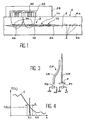
- the optical fiber 2 of single-mode preference, is provided with one or more sensors 4 which, in the example shown, are Bragg grating transducers photo-inscribed on the fiber 2.
- transducers allow measure deformations or variations in temperature of a composite material structure 6 in which the system S is integrated (micro-system substantially plane in the example shown) and the optical fiber 2 provided with one or a plurality of transducers 4.
- the fiber does not has only one transducer 4 and the micro-system substantially plane S can then be formed on a insulating substrate 10 (FIG. 1) which can be rigid (for example glass or silicon) or otherwise flexible (for example polyimide).
- a insulating substrate 10 (FIG. 1) which can be rigid (for example glass or silicon) or otherwise flexible (for example polyimide).
- fiber 2 has several transducers 4, for example eight transducers that are placed in series on this fiber 2.
- the substrate 10 of the micro-system S can be a "smart" substrate, by example of glass or silicon, using the integrated optics techniques for the manufacture of microwave system.
- This micro-system S comprises a circuit optical 12 and an electronic circuit 14.
- the optical circuit 12 also includes opto-electric means 20.
- Source 16 is connected to a channel input of the coupler 18.
- the other input channel of this coupler 18 is connected to the opto-electric means 20.
- One of the two output channels of the coupler 18 is left free and split at an angle to cancel the reflections at the end of the fiber.
- the other end of the optical fiber 2 is cleaved at an angle.
- Source 16 sends the light she generates in optical fiber 2 and optoelectrical means 20 detect the modified light by each transducer 4 in response to variations of temperature or to deformations of the structure 6 and provide electrical signals to determine these temperature variations or these deformations.
- These feed means 24 receive from energy by electromagnetic induction and comprise for this purpose a substantially flat coil 26 ( Figure 1).
- This plug-in 28 is intended to be in contact with the outer wall of the structure 6.
- the high voltage power supply means (100 to 200 Vrms) and high frequency include a coil 30 associated with a core 32 which serves to guide the field lines to the coil 26 of the micro-system.
- the coil 30 constitutes a primary coil and the coil 26 constitutes a secondary coil.
- the core 32 is preferably nickel-zinc.
- This plug-in can be attached to the wall external structure 6 to power the micro-system and receive the signals continuously when the use of the structure.
- This second use is preferable because it does not add to the structure any element additional risk of disturbing both the manufacture of this structure and the operation of it.
- micro-system substantially plane S is integrated between two webs 6a and 6b of the composite material.
- the typical dimensions of this micro-system are 25 mm x 80 mm x 2 mm.
- the substrate 10 can be attached to a flexible support 34, for example polyimide (FIG. 1) which extends the substrate 10 and makes it possible to position the optical fiber 2 at the edge of this substrate 10.
- a flexible support 34 for example polyimide (FIG. 1) which extends the substrate 10 and makes it possible to position the optical fiber 2 at the edge of this substrate 10.
- the composite material can be carbon-epoxy or kevlar (registered trademark) -epoxy.
- the typical manufacturing process of a carbon-epoxy composite material in an autoclave requires a temperature of 180 ° C. and a pressure of the order of 7 ⁇ 10 5 Pa for several hours.
- micro-system S as well as its substrate 10 and the possible support 34 are of preferably embedded in a coating element 36 of the type ceramic or epoxy.
- a ceramic is used marketed under the reference COTRONICS 808.
- thermal expansions of this ceramic, carbon-epoxy and kevlar (registered trademark) -epoxy are respectively of the order of 2.5x10 -6 / ° C, 0.5x10 -6 / ° C and -2x10 -6 / ° C (in the case of woven cross-fibers with identical characteristics in two dimensions).
- This ceramic will undergo a slight shrinkage when cooling to room temperature at the exit of the autoclave.
- the transducer 4 provides from the light that it receives from the source 16 a spectral line susceptible to fluctuate in a given spectral domain.
- Optoelectric means 20 include an optical coupler CO having two branches which are respectively a route of VM measurement and a VR reference channel.
- the spectral line is sent to the branch input from this coupler via the channel Corresponding coupler 18.
- the VM measurement channel has a filter optical F (wavelength selective element) having a known response and a strong spectral transition.
- This filter F is followed by a photodetector P1 which provides an electrical signal s1 representative of the light filtered by this filter.
- Another photodetector P2 is placed at the following the VR reference path and provides a signal s2 electrical representative of the light transmitted by it.
- the transducers 4 provide spectral lines that are likely to fluctuate respectively in spectral domains determined.
- the means opto-electric devices 20 include a device demultiplexing and filtering 40 and a bar of photodiodes 42.
- the device for demultiplexing and filtering 40 forms an integrated optical circuit plane whose the entrance is connected to the corresponding branch of coupler 18 for receiving the spectral lines and whose the outputs respectively provide the lines spectral parameters demultiplexed so that they can then be measure the respective wavelengths of these lines spectral.
- the demultiplexing device described makes it possible to measure eight wavelengths of eight photo-inscribed Bragg transducers on the single mode fiber 2.
- each exit is divided into a path of measurement equipped with a filter and a reference channel.
- each demultiplexed spectral line is also sent to the input branch of a CO optical coupler, both of which output branches respectively constitute the path VM and the VR reference channel and we use also a photodiode connected to the measuring channel, which is equipped with an optical filter, and another photodiode connected to the reference path.
- the bar 42 thus comprises at least 8 pairs of photodetectors since there are 8 lines spectral data to be observed (from the 8 transducers Bragg of fiber or line of measurement).
- the bar may include a larger number of photodetectors (eg 256, 512 or 1024), each guide output being able to transmit on several photodetectors.
- photodetectors are then placed electrically in parallel in order to summon their photocurrent.
- the ratio s1 / s2 can be determined electronically by a conformer using logarithmic and anti-logarithmic amplifiers or by an analog divider.
- This report can also be determined digitally by a computer after converting signals s1 and s2 in digital form by means of a analog-digital acquisition card.
- the spectral line of a Bragg transducer is well approximated by a Gaussian profile centered on a wavelength ⁇ i (FIG. 4) that can be measured and having a characteristic width ⁇ and thus a width at half-height 2. (1n2) 1/2 . ⁇ .
- Figure 4 shows the variations of the transmission T ( ⁇ ) of the filter, expressed as a percentage, according to the wavelength ⁇ .
- the spectral width ⁇ has been represented at inside which the line ⁇ i can vary.
- the substantially rectilinear part I of T ( ⁇ ) is contained in a line that has slope A and intersects the axis of ⁇ in ⁇ 0.
- the filter F can be a filter transition or a bandpass filter.
- It can be a colorful filter (working by absorption) or a multilayer filter dielectric (working by interference).
- the superluminescent diode 16 of the figure 2A (whose spectral width may be a few tens of nanometers) can be replaced by a electroluminescent diode having a spectral width of the order of a few nanometers.
- Such diodes are commercially available at the wavelengths used for optical telecommunications (1550 nm and 1350 nm) but also at other wavelengths like for example 820 nm.
- the optical spectrum of these diodes has a Gaussian look and a spectral width typical of About 30 nm.
- the solution used in the example of FIG. 2B consists in producing an optical circuit specific which is optically integrated on a substrate in glass or on a silicon substrate.
- substrates that are typically 1 mm thick.
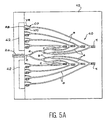
- Figure 5A is a view from above schematic of these means of demultiplexing and filtering 40 while Figure 5B is a view of schematic and partial top of a variant of realization of these.
- the means of demultiplexing and filtering represented in FIGS. 5A and 5B have eight corresponding demultiplexing channels respectively to the eight multiplexed transducers in the spectrum of the superluminescent diode (see Figure 6B).
- the length of the component forming the means of demultiplexing and filtering is about 5 cm for a width of about 5 mm.
- the means of demultiplexing and filtering also have an additional part that puts in the already described filter measurement principle higher and applied in this case to optics integrated flat.
- the principle of this technique consists in exchanging alkaline ions (for example Na + ions) which are already present in the glass with other ions (for example Ag + or Tl + ) which have the effect of locally increasing the refractive index of glass.
- alkaline ions for example Na + ions
- other ions for example Ag + or Tl +
- This technique consists in spreading a first doping in the glass substrate in the field electric.
- PECVD plasma enhanced chemical vapor deposition
- a silica layer On a silicon substrate, a silica layer whose thickness is about 8 microns.
- a layer of silica doped with phosphorus forming the heart of the guides (whose thickness is equal at 9 ⁇ m) is then deposited and etched.
- the advantage of integrated optics silicon is to be able to simultaneously etch V-shaped grooves for fiber positioning single-mode optical.
- Each separating junction can be a Coupler adjusted to 50% (3 dB).
- each separating junction is preferably a Y junction.
- Such a junction has the advantage to be achromatic and to be independent of the polarization of light.
- the means of demultiplexing and filtering represented in FIGS. 5A and 5B use such junctions Y.
- the proportion of light energy incident on the photodiode array 42 is of the order of 6% of the light energy injected into the means of demultiplexing and filtering 40.
- junction referenced a As seen in FIG. 5A, since it is desired to separate eight spectral lines, seven cascaded Y junctions are used, namely a junction referenced a , two junctions referenced b and four junctions referenced c .
- the input branch of the junction a is optically coupled to the corresponding branch 2a of the coupler 18 (FIG. 2B) to constitute the input e of the set of junctions.
- the two output branches of this junction a are respectively coupled to the input branches of the two junctions b .
- Each of the output branches of these junctions b is itself coupled to the input branch of one of the four junctions c .
- junctions c constitute the outputs of the set of junctions which are respectively coupled to eight Bragg gratings r .
- Each of these Bragg gratings forms a selective light reflector in wavelength.
- This light reflector has a band wavelength that contains the domain spectral in which one of the eight spectral lines is likely to fluctuate.
- Each of the Bragg gratings r is not only coupled on one side to one of the outputs of the set of junctions a, b, c but also coupled, by the same side to an optical waveguide o which is intended to propagate the light corresponding to the demultiplexed line, reflected by this Bragg grating.
- Each waveguide o is coupled to the input branch of the corresponding CO coupler used for filtering.
- the optical fiber 2 is single-mode at the wavelength of use that is typically equal to 1300 nm, 1550 nm or 820 nm.
- the core of the optical fiber 2 is doped with GeO 2 and this fiber may be polarization-maintaining or not.
- Bragg's networks are photo-inscribed sensitive optical fiber 2 (to serve as transducers) and on the guides of the means of demultiplexing and filtering 40.
- Bragg networks can be do two ways: one can either etch chemically the previously thinned sheath of a guide so that this sheath is flush with the heart of the guide is practicing a photo-inscription as described in the documents (22), (23) and (24).
- the glass manufacturing process includes an annealing that makes the glass very little photosensitive by removing structural defects.
- Preferential optical registration mode networks is the method of the phase mask.
- Photo-inscribed demultiplexing networks are networks with variable period like this is described in documents (25) and (26).
- the spectral width useful is about 1 nm to 1.3 ⁇ m (which corresponds to a maximum deformation of 1000 ⁇ exerted on the structure 6).
- the spectral shift induced by thermal derivative is approximately ⁇ 0.5 nm (which corresponds to a thermal drift of +/- 50 ° C).
- FIGS. 6A and 6B In this regard, reference is made to FIGS. 6A and 6B.
- Measurement filters can be Bragg gratings with variable periods (Figure 5A), of which the operating point is on a flank of their spectral response, or multilayer filters dielectrics (Figure 5B) that function as transition filters (high pass or low pass).
- the Bragg networks transducers and the micro-system are not at the same temperature, it is possible to provide a network of Bragg that serves as a reference for the temperature and which is not subject to constraints in the material composite.
- one solution is to insert optical fiber 2 into a polymer sleeve (Teflon) before insertion of this fiber into the composite material.
- Multilayer deposition involves depositing a layer of photosensitive resin on the substrate (for example by electrostatic or quenching) and Masking to develop an area out of two.
- the filter F can to be a Fabry-Perot type optical filter (multilayer) bandpass spectral transmission which provides a slope of about 25% per nanometer.
- the accuracy of deformation measurement by a transducer is to a few tens of ⁇ .
- the measurement range is 1000 ⁇ for each of the eight transducers.
- each waveguide o is coupled to the input branch of the corresponding CO coupler, which is part of the filtering device.
- the branch of VM output of this coupler carries a Bragg grating to variable periods RB serving as a filter.
- branches VM output results in multilayer filters identical dielectrics FU, each FU filter being common to two adjacent VM branches in the example represent.
- a filter with spectral transition of high pass or low pass ensures a slope of the order of 2.5% per nanometer.
- the resolution is then of the order of 100 ⁇ for each transducer.
- the spectral width of each of these rays is for example of the order of 0.2 nanometers.
- the light that we want to demultiplex is separated, in a balanced way from the point of view of the luminous energy, by all the junctions Y.
- each of the outputs of the set of Y junctions resulted in a demultiplexing Bragg grating r serving as a reflector over the entire spectral band of measurement of each of the transducers.
- FIG. 6B shows the respective spectral transfer functions F ( ⁇ i ) of the eight demultiplexing Bragg gratings where i varies from 1 to 8, each of these functions containing the spectral domain of evolution of a line (spectral width of the order of 0.2 nm) of the optical spectrum of the incident light energy.
- the spectral width at -3 dB is of the order of 3 nanometers for each function of spectral transfer.
- Figure 6B also shows the spectrum of superluminescence II of the diode that excites transducer Bragg gratings and whose width spectral is of the order of 30 nanometers to 50 nanometers.
- spectral III which is common to all filters at dielectric multilayers (high-pass filters in the example shown in Figure 6B).
- Bragg gratings could be replaced by means of demultiplexing with etched network or network PHASAR microguides.
- filtering could be done by means of dielectric multilayer filters different from each other, respectively associated to measurement channels, or by means of interferometers Mach-Zehnder interferometer.
- the electronic circuit 14 includes the transmission means 22 and the power supply means 24 electrical transmission means 22 and the diode superluminescent 16 forming part of the optical circuit 12.
- These feeding means 24 comprise, as we have seen, the secondary coil 26.
- the external module 28 includes the coil primary 30, means 52 for feeding this primary coil and means 54 for receiving the signals emitted by the transmitting means 22.
- Figure 7 also shows means 56 for processing the signals provided by these receiving means 54 and means 58 of visualization of the results obtained by these means of treatment 56.
- the feeding means 24 are such that shown in Figure 7 and therefore include the secondary coil 26 associated with a capacity of agreement Cs, a diode D, a capacitance C and a transistor of regulation T which is provided with a basic resistance Rb, a Zener diode Dz and a current source Sc.
- the means 52 for feeding the coil primary 30 are as shown in FIG. and therefore include a primary oscillator 58, whose frequency is for example 28 kHz, a transformer-generator 60 whose primary circuit is powered by the oscillator 58 via an amplifier 62.
- the secondary circuit of this transformer 60 feeds the primary coil 30 via of an adjustable Raj resistor and a chord capacity Cp associated with the primary coil 30.
- the first way is to use a paired tuned circuit and that's what we see on the figure 7 while the second way is to use a purely inductive transformer (without ability to agree).
- This filter which is called “ ⁇ filter”
- ⁇ filter consists of a series inductance and two capacity to ground and has a frequency of cut on the order of 1 to 10 kHz.
- the apparent load resistance R'c seen by the coil secondary 26 is equal to a quarter of the resistance Rc of load of the order of 60 ⁇ .
- this apparent load resistance is equal to half of Rc.
- L represents the inductance
- C the capacitance
- This quality factor Q of this oscillator depends on the resistance of the primary circuit and the resistance R of the secondary circuit brought back to the circuit primary.
- the secondary oscillating circuit is constituted by the secondary coil 26 (for example "microstrip” coil type), whose total inductance is noted Ls, and the capacity of agreement Cs.
- the basic resistance Rb of the transistor of T regulation is of the order 1 k ⁇ .
- the zener diode DZ is intended to maintain the base of the transistor at a constant potential typically a few volts.
- the emitter of this transistor feeds the transmission means 22 (voltage Vcc) while the diode superluminescent 16 is powered by the source of current Sc of the order of 50 mA.
- Such a power source is commercially available for example under the reference LM134.
- It can be a field effect transistor whose gate is connected to the drain by a polarization resistance.
- the voltage is then applied to the source of this field effect transistor and the current stabilized is taken after resistance (on the door).
- the circuit consisting of the Zener diode, the polarization resistor and the transistor exists in a standard way.
- the transfer function is a bandpass function centered on the frequency of resonance that depends on the resistance according to the formula (1).
- the signal modulation frequency at the circuit level primary can also be adjusted.
- induction feeding which consists of a purely inductive transformer is identical to what is shown in Figure 7 except that the Cp and Cs capabilities are removed.
- the energy coupling is good less selective in frequency.
- the power setting is then by Raj resistance or by changing the voltage of the oscillator 58.
- This transformer has, like "gap", the composite material for example carbon-epoxy type whose magnetic permeability is very close to 1.
- the winding ratio is of little importance because the desired application is the transfer energy.
- This winding ratio is set by the dimensioning constraints knowing that the number of turns of the secondary coil is limited (by the traditional photoengraving capacity) to around a hundred turns (see document (27)), the width of a turn and the interval between turns being the order of 50 microns to 100 microns.
- This secondary coil can be realized by the classical technique of printed circuits.
- the inductances then obtained are of the order of a few tens of ⁇ H for about 50 turns and outer diameters of the order of 2 cm to 3 cm.
- the secondary inductance being limited by the technique of photo-etching a few dozen ⁇ H, a primary coil is advantageously used very strong inductance in order to increase the mutual inductance.
- V dry V pri K.
- the p The s . ⁇ R 2 p + L 2 p . ⁇ 2
- Ls represents the total inductance of the secondary coil
- Lp represents the total inductance of the primary coil
- Rp represents the resistance of this primary coil
- ⁇ represents the pulsation of the oscillator
- K represents the coupling coefficient
- the transformation ratio in coupling loose is directly a function of the coefficient of K coupling of the flow sharing between the coils primary and secondary.
- the ratio of vacuum transformation is of the order of 80 to 100.
- the equivalent transformer is characterized by strong leakage inductances because the magnetic circuit is looped largely by air and material composite.
- the reluctance of the magnetic circuit useful is comparable - even stronger - than the Reluctance of leaks.
- M 2 K 2 .L p .L s.
- ⁇ is the excitation pulse (expressed in radians per second)
- R s is the resistance of the secondary coil
- R c ' is the load resistance formed by the electronic circuit 14.
- the optimal load resistance is order of a few ohms.
- Load impedance is defined by the current source Sc which supplies the diode superluminescent 16.
- the load resistance is worth about 60 ⁇ .
- This secondary load resistance is therefore adapted.
- the maximum coupled power is of the order of 400 mW for this load resistance of the order of 60 ⁇ .
- the power is slightly less than 200 mW.
- This power exceeds the minimum of required power (of the order of 100 mW) so that the Power setting is not critical.
- This increase in frequency allows so to compensate for the lower inductance of the secondary coil within the limits of energy losses by eddy currents and by hysteresis in the composite material and the core 32 as well as in modulation limits imposed by the frequency of cutting of coils and the effect of skin in yarns conductors above 1 MHz.
- the core 32 is chosen in Frequency domain function considered.
- the photo-diodes operate in a photo-conductive regime to provide a linear voltage depending on the incident optical power.
- each photo-diode is connected to the input of a trans-impedance type circuit TI schematically illustrated in Figure 8 and using an Rconv conversion resistance of the order of a few hundred k ⁇ to 1 M ⁇ .
- V Rconv.Iph
- Iph is the current photo which is directly a function of the optical flow received by the photodiode Pd corresponding to the considered assembly.
- the conversion box 70 being part transmission means 22, examples of which are schematically represented in FIGS. 9A, 10A and 11A ensures this conversion of the intensity into voltage for all photo-diodes.
- this conversion box 70 therefore comprises two trans-impedance montages TI.
- this conversion box 70 includes 2N assemblies of trans-impedance TI (N being equal to 8 since uses 8 transducers in the example).
- each assembly of trans-impedance TI includes an amplifier 72 whose input - is connected to the anode of the associated photo-diode Pd and whose input + is connected to the cathode of this photo-diode Pd.
- the conversion resistance associated with Rconv connects the input - of this amplifier 72 to the output of this one.
- the transmission means 22 are subject to a strong constraint of optimization of the sizing geometric and electrical consumption.
- the first particular embodiment uses a time multiplexing of signals followed frequency modulation.
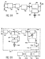
- FIG. 9A This first particular embodiment is schematically represented in FIG. 9A for the transmission means and in FIG. 9B for the associated reception means in the case of the example of the invention shown in Figure 2A (single transducer).
- FIG. 10A This first particular embodiment is schematically shown in Figure 10A for the transmission means and in FIG. 10B for the associated reception means in the case of the example of the invention shown in Figure 2B (multiple transducers: 8).
- the second particular embodiment uses a carrier amplitude modulation multiples, followed by frequency modulation.
- This second particular embodiment is schematically shown in Figure 11A for the transmission means and in FIG. associated receiving means.
- the frequencies carriers are between 800 MHz and 1000 MHz equal to 2.45 GHz or even 5.8 GHz.
- This phase locked loop 84 is equipped with a crystal oscillator 86.
- the transmission means of FIG. 9A also include a transmitting antenna 88 which is connected to the output of oscillator 80 and to the input of the loop 84.
- the set consisting of the multiplier 105, of the phase locked mouth 108 and its 110 crystal oscillator, and the controlled oscillator in voltage constitutes a frequency demodulator.
- the reception means 54 comprise also another frequency demodulator 114 (frequency f1) which receives as input the output signal of the filter 112 and which outputs the signal demodulated (in baseband).
- This signal is then processed in the means 56.
- this signal (in the form analogue) is converted to digital form by a analog-to-digital converter 56a whose signal output is processed by a computer 56b that allows to calculate the wavelength of the spectral line corresponding to the single sensor 4 of Figure 2A in a way explained above.
- the measurands that is to say the parameters to measure (temperature, deformation) are then calculated through the behavioral relations of Bragg gratings (see references (1) or (3)).
- Data is sent out of the composite material by frequency modulation for to overcome the attenuation by the material.
- the local oscillator 97 can be a controlled voltage oscillator of the kind of the one that is marketed by the company Murata under the reference MQE000.
- the divider 76 may be an integrated circuit of the kind that is marketed by society Burr-Brown under the reference MPY600.
- the transmission means 22 of FIG. 10A include a conversion box 70 which receives in input the signals of the N couples of photodiodes forming the bar 42 of FIG. 2B (N being example equal to 8 as we have seen) and which provides in output N pairs of measurement and reference signals.
- the means 22 of FIG. 10A comprise also a multiplexer 118 which receives in input the signals of the dividers 116 and which is controlled by a counter 120 provided with a clock 122.
- the transmission means 22 of FIG. 10A further include the oscillator 78, the oscillator 80, the multiplier circuit 82, the phase lock 84 and the crystal oscillator 86 as well as the antenna 88, arranged as in FIG. 9A, the input of the oscillator 78 being connected to the output of the multiplexer 118 in the case of Figure 10A.
- the receiving means 54 of FIG. 10B are identical to the receiving means 54 of the figure 9B and are still provided with the antenna 90.
- the output signals from the means 54, from the demodulator 114 are sent to analog-to-digital converter 124 and comparator 130 which also receives a voltage input VS threshold set by the users in order to trigger on all pulses from the receiver in frequency modulation 54.
- the reception means 22 of FIG. 10B also include a 56b computer that processes output signals from the parallel register 128 for calculate the values of the wavelengths of the lines spectral corresponding to the sensors 4 of the figure 2B.
- the measurands (temperature, deformation) are then calculated through behavioral relationships Bragg networks.
- the means 58 display the measurands thus calculated.
- FIGS. 10A and 10B the signals are sequentially observed.
- a coding for registering the transducers 4 is necessary (timing).
- a possible solution consists in using, as a counter 120, a counter by 16 (for eight transducers 4).
- the transmitted signal is constituted of a bit 1 of identification (reference br in FIG. 10A), of seven bits at zero and signal consisting of sampling eight signals to transmit.
- the signals After reception, the signals are used to trigger the analog-to-digital conversion.
- the tracking bit 1 is detected in redeclining the monostable 132 (of duration T slightly greater than the period of the pulses of the clock) and by setting this monostable to zero at each pulse.
- the trigger pulse appears at the output of monostable 132 as soon as there is more pulse.
- This pulse is used to authorize the transfer of the contents of the serial register 126 into the parallel register 128 for this content to be read by the computer 134 at each scan cycle.
- This impulse can also be used to manage interrupting the computer referenced 56b (the parallel register 128 not being useful in this case).
- the transmission means 22 of FIG. 11A still include the associated conversion box 70 to the N couples of photodiodes as well as the N dividers 116 whose inputs are connected to the outputs of the conversion box 70 as in the case of the figure 10A.
- Means 22 of FIG. 11A comprise also N digital-to-analog converters 136 as well that a logical interface 138 to N outputs.
- This logical interface 138 receives in input of signals from a clock 140 to 900 MHz, associated with a quartz oscillator 142.
- the transmission means 22 of FIG. 11A also include N bandpass filters 144 whose respective central frequencies are the frequencies f1, f2, ..., fN and whose inputs are respectively connected to the outputs of digital-to-analog converters 136.
- the receiving means 54 of FIG. 11B are identical to the receiving means 54 of the figure 9B and are still provided with the receiving antenna 90.
- the output of these means 54 constituted by the output of the demodulator 114 (FIG. 9B) is connected to the processing means 56.
- N bandpass filters 148 which include N bandpass filters 148 whose center frequencies are respectively f1, f2, ..., fN and the output of the demodulator 114 of the means 54 is connected to the input of each filter 148.
- N amplitude demodulators 150 whose frequencies of heterodynage are respectively f1, f2, ..., fN and whose entries are respectively related to filters 148.
- the processing means 56 of the figure 11B also include an analog-to-digital converter 152 having N inputs respectively connected to the N outputs of the demodulators 150.
- the output signals of this converter analog-digital 152 are sent to a computer 56b which calculates the wavelengths of the lines spectral transducers 4 of Figure 2B and deduce the values of the measurands.
- the results of the calculations are displayed by the display means 58.
- bass carrier frequencies can be generated without to use any large discreet component (in which case significant capacities and inductances would be necessary) and that these frequencies can be precisely.
- the amplitude demodulators 150 can consist of mixers (at frequencies f1, f2, ..., fN) followed by low-pass filters.
- the present invention applies more particularly in situ monitoring of "smart" structures.
- Aeronautics is one of the sectors preferred application of this invention.
- the system object of the invention can be used, it can be cite the radomes as well as the veins and the wing wings of planes.
- This system is not only usable with composite materials.
- non-magnetic materials having a permeability relative magnetic field substantially equal to 1
- the invention can then for example apply to the surveillance of buildings and dams.
- the first solution uses a Y junction with a Bragg grating r (advantageously at 100% of reflection) photo-inscribed on the input branch (see Figure 12A where the junction has the reference J).
- This solution is advantageous in that the properties guiding Y-junctions are very insensitive to the polarization and at the wavelength of light. Thus, only one mask can be made to obtain the component making manufacturing very flexible because only the wavelengths of the Bragg gratings are adjusted to make the demultiplexer.
- this Y junction imposes an optical loss of 6 dB when of the filtering operation (i.e. the signal go from the exit s to the guide o).
- a second solution to overcome this drawback is to simultaneously photo-register each Bragg grating r (preferably 100% reflection) on the two arms of a coupler K to form a network-assisted coupler (see Figure 12B).
- the principle of a network-assisted coupler is then the following.
- the coupling length, the coupling interval and the characteristics of the coupler guides are chosen so as to obtain a total transfer of the energy from port I to coupled port III, ie 100%.
- Point 1 establishes immunity to drifts thermal effects affecting the entire structure to monitor, and point 2) immunity to drifting resulting from thermal inhomogeneities within this structure, which frequently happens in large structures.
- the choice frequency modulation transmission of information to the outside of the structure guarantees transmission of information independent of energy losses unlike a system that uses amplitude modulation. Immunity to drifting must be ensured for any system intended to to operate over long periods of time (a few minutes to a few years).
- the information transmitted is a quotient between the intensity transmitted by a measurement filter and the reference intensity, this quotient being proportional to the measured wavelength difference regardless of the value of the light intensity.
- the invention therefore allows a standardized measurement.
- the system which is the subject of the invention is therefore particularly suitable for measurements at frequencies high (kHz and above) and also allows you to perform measurements at low or very low frequencies, guaranteeing immunity to thermal drifts previously described.
- Industrial applications corresponding are the watch over time of mechanical structures, especially large ones, and especially the monitoring of structures aircraft. Supervision of civil engineering works also suitable.
Landscapes
- Physics & Mathematics (AREA)
- General Physics & Mathematics (AREA)
- Investigating Or Analysing Materials By Optical Means (AREA)
- Optical Couplings Of Light Guides (AREA)
- Arrangements For Transmission Of Measured Signals (AREA)
Description
- un circuit optique comprenant une source de lumière, qui est prévue pour envoyer ladite lumière dans la fibre optique, et des moyens opto-électriques prévus pour détecter la lumière modifiée par le capteur et fournir des signaux électriques permettant de déterminer la modification du paramètre de la structure, et
- un circuit électronique comprenant des moyens d'émission radio-fréquence de ces signaux électriques et des moyens d'alimentation qui reçoivent de l'énergie électromagnétique par induction et sont prévus pour l'alimentation électrique de la source de lumière et des moyens d'émission radio-fréquence,
- un séparateur en énergie, ayant une entrée, qui est destinée à recevoir le spectre optique formé par l'ensemble des raies spectrales, et une pluralité de sorties qui sont aptes à fournir respectivement des fractions de l'énergie lumineuse du spectre optique, et
- une pluralité de réflecteurs de Bragg sélectifs en longueur d'onde qui sont respectivement reliés aux sorties, chaque réflecteur de lumière sélectif en longueur d'onde ayant une bande passante en longueur d'onde qui contient le domaine spectral associé à l'une des raies et réfléchissant donc seulement cette raie, chaque réflecteur sélectif étant relié à un guide d'onde optique destiné à propager la raie réfléchie par ce réflecteur.
- un dispositif de mesure, par filtrage, de la longueur d'onde de chaque raie spectrale, ce dispositif de mesure comprenant, pour chaque raie, une voie de mesure munie d'un filtre et une voie de référence, et
- des moyens de photo-détection, pour chaque raie spectrale, des intensités lumineuses respectivement transmises par les voies de mesure et de référence correspondantes, de manière à pouvoir déterminer la longueur d'onde de cette raie en calculant le rapport des intensités ainsi détectées.
- des moyens d'émission d'énergie électromagnétique destinée à être fournie, par induction, aux moyens d'alimentation faisant partie du circuit électronique du système,
- des moyens d'alimentation à haute tension et haute fréquence de ces moyens d'émission d'énergie électromagnétique, et
- des moyens de réception des signaux émis par les moyens d'émission radio-fréquence faisant partie du circuit électronique du système.
- la figure 1 est une vue en coupe schématique d'un mode de réalisation particulier du système objet de l'invention,
- la figure 2A est une vue schématique d'un système conforme à l'invention, associé à un seul capteur,
- la figure 2B est une vue schématique d'un autre système conforme à l'invention, associé à plusieurs capteurs,
- la figure 3 illustre schématiquement le principe d'une mesure de longueur d'onde utilisable dans l'invention,
- la figure 4 représente les variations de la transmission d'un filtre utilisable pour la mise en oeuvre de l'invention, en fonction de la longueur d'onde,
- les figures 5A et 5B sont des vues de dessus schématiques de moyens de démultiplexage en longueur d'onde utilisables dans l'invention,
- les figures 6A et 6B illustrent schématiquement le principe d'un démultiplexage spectral utilisable avec le système de la figure 2A (pour la figure 6A) et avec le système de la figure 2B (pour la figure 6B),
- la figure 7 est une vue schématique du module associé au système de la figure 1 et du circuit électronique faisant partie de ce système,
- la figure 8 est un schéma électrique d'un circuit de conversion courant-tension de type transimpédance utilisable dans l'invention,
- la figure 9A est une vue schématique d'un mode de réalisation particulier de moyens d'émission radiofréquence utilisables dans un système conforme à l'invention et la figure 9B est une vue schématique de moyens de réception qui leur correspondent dans le module associé à ce système,
- la figure 10A est une vue schématique d'un mode de réalisation particulier de moyens d'émission radiofréquence utilisables dans un autre système conforme à l'invention et la figure 10B est une vue schématique de moyens de réception qui leur correspondent dans le module associé à cet autre système,
- la figure 11A est une vue schématique d'un mode de réalisation particulier de moyens d'émission radiofréquence utilisables dans un autre système conforme à l'invention et la figure 11B est une vue schématique de moyens de réception qui leur correspondent dans le module associé à cet autre système,
- les figures 12A et 12B illustrent schématiquement deux possibilités de démultiplexage, et
- la figure 13 illustre schématiquement un autre mode de réalisation particulier de l'invention.
- une source de lumière 16 formée par une diode superluminescente et
- un coupleur optique équilibré à quatre voies 18 (50% de transmission sur les deux voies de sortie).
- des moyens 22 d'émission radio-fréquence de ces signaux électriques et
- des moyens 24 d'alimentation électrique de la source de lumière 16 et des moyens d'émission radio-fréquence 22.
- des moyens d'émission d'une énergie électromagnétique destinée à être fournie par induction électromagnétique aux moyens 24 d'alimentation faisant partie du circuit électronique 14 du micro-système S,
- des moyens d'alimentation à haute tension et haute fréquence de ces moyens d'émission d'énergie électromagnétique et
- des moyens de réception des signaux émis par les moyens d'émission radio-fréquence 22 du micro-système S.


- le boítier de conversion 70 ayant deux entrées respectivement reliées aux deux photodiodes P1 et P2 de la figure 2A et deux sorties fournissant respectivement un signal de mesure et un signal de référence,
- un diviseur 76 qui reçoit en entrée ce signal de mesure et ce signal de référence et qui fournit en sortie un signal égal au rapport de ce signal de mesure à ce signal de référence,
- un oscillateur contrôlé en tension 78 (autour de la fréquence notée f1) qui reçoit en entrée le signal de sortie du diviseur 76,
- un autre oscillateur contrôlé en tension 80 (autour de la fréquence porteuse notée fp),
- une boucle à verrouillage de phase 84 dont l'entrée est reliée à la sortie de l'oscillateur contrôlé en tension 80, et
- un circuit multiplicateur 82 dont les deux entrées sont respectivement reliées aux sorties de l'oscillateur 78 et de la boucle à verrouillage de phase 84.
- un filtre passe-bande 92 qui a comme fréquence centrale la fréquence notée fp et dont l'entrée est reliée à cette antenne 90,
- un circuit multiplicateur dont une entrée est reliée à la sortie du filtre 92 par l'intermédiaire d'un amplificateur 96,
- un oscillateur local 97 à une fréquence notée fOL,
- une boucle à verrouillage de phase 98 associée à cet oscillateur 97 et munie d'un oscillateur à quartz 100, le circuit multiplicateur recevant à sa deuxième entrée le signal de sortie de l'oscillateur local 97,
- un filtre passe-bande 102 qui a comme fréquence centrale une fréquence intermédiaire notée fI égale à fOL-fp et qui est relié à la sortie du circuit multiplicateur 94 par l'intermédiaire d'un autre amplificateur 104,
- un autre circuit multiplicateur 105 dont une entrée est reliée à la sortie du filtre 102,
- un autre oscillateur contrôlé en tension 106 autour de la fréquence fI dont la sortie est reliée à l'autre entrée du circuit multiplicateur 105,
- une autre boucle à verrouillage de phase 108 dont l'entrée est reliée à la sortie de ce circuit multiplicateur 105 et qui est munie d'un oscillateur à quartz 110 et
- un filtre passe-bande 112 qui a comme fréquence centrale la fréquence f1 et dont l'entrée est reliée à la sortie de la boucle à verrouillage de phase 108 et à l'entrée de l'oscillateur contrôlé en tension 106.
- un convertisseur analogique-numérique 124,
- un régistre série 126,
- un registre parallèle 128,
- un comparateur 130, et
- un monostable redéclenchable 132 qui sont agencés comme cela est représenté sur la figure 10B.
- être toutes incluses dans la source d'excitation spectralement large (par exemple diode super luminescente)
- être suffisamment distinctes pour une bonne séparation des voies de mesure dans un dispositif de démultiplexage du genre de celui qui a été décrit plus haut.
Claims (20)
- Système d'alimentation et de transmission pour capteur à fibre optique, intégré dans une structure (6) en matériau amagnétique, la fibre optique (2) étant reliée à au moins un capteur (4) apte à modifier une lumière se propageant dans cette fibre optique (2), sous l'effet d'une modification d'un paramètre de la structure (6), chaque capteur (4) étant un transducteur à réseau de Bragg,
ce système étant caractérisé en ce qu'un circuit optique (12) et un circuit étectronique sont intégrés dans ladite structure (6),
le circuit optique (12) comprenant une source de lumière (16), qui est prévue pour envoyer ladite lumière dans la fibre optique (2), et des moyens opto-électriques (20) prévus pour détecter la lumière modifiée par le capteur (4) et fournir des signaux électriques permettant de déterminer la modification du paramètre de la structure (6), et
le circuit électronique (14) comprenant des moyens (22) d'émission radio-fréquence de ces signaux électriques et des moyens d'alimentation (24) qui reçoivent de l'énergie électromagnétique par induction et sont prévus pour l'alimentation électrique de la source de lumière (16) et des moyens (22) d'émission radio-fréquence. - Système selon la revendication 1, dans lequel chaque transducteur à réseau de Bragg est photo-inscrit sur la fibre optique (2).
- Système selon l'une quelconque des revendications 1 et 2, dans lequel chaque capteur (4) est apte à fournir, à partir de ladite lumière, une raie spectrale susceptible de fluctuer dans un domaine spectral déterminé en vue de mesurer la longueur d'onde de cette raie.
- Système selon la revendication 3, dans lequel la fibre optique (2) est munie d'une pluralité de capteurs (4) placés en série sur cette fibre optique (2), les moyens opto-électriques (20) comprenant un dispositif de démultiplexage (40) ayant une entrée destinée à recevoir les raies spectrales correspondant aux capteurs (4) et des sorties destinées à fournir respectivement les raies spectrales démultiplexées de façon à pouvoir mesurer les longueurs d'onde respectives de ces raies.
- Système selon la revendication 4, dans lequel le dispositif de démultiplexage (40) comprend :un séparateur en énergie (a, b, c), ayant une entrée, qui est destinée à recevoir le spectre optique formé par l'ensemble des raies spectrales, et une pluralité de sorties qui sont aptes à fournir respectivement des fractions de l'énergie lumineuse du spectre optique, etune pluralité de réflecteurs de lumière sélectifs en longueur d'onde (r) qui sont respectivement reliés aux sorties, chaque réflecteur de lumière sélectif en longueur d'onde ayant une bande passante en longueur d'onde qui contient le domaine spectral associé à l'une des raies et réfléchissant donc seulement cette raie, chaque réflecteur sélectif étant relié à un guide d'onde optique destiné à propager la raie réfléchie par ce réflecteur.
- Système selon la revendication 5, dans lequel le séparateur en énergie (a,b,c) est un ensemble de jonctions séparatrices montées en cascade.
- Système selon l'une quelconque des revendications 5 et 6, dans lequel les réflecteurs sélectifs comprennent des réseaux de Bragg.
- Système selon l'une quelconque des revendications 3 à 7, dans lequel les moyens opto-électriques (20) comprennent :un dispositif de mesure, par filtrage, de la longueur d'onde de chaque raie spectrale, ce dispositif de mesure comprenant, pour chaque raie, une voie de mesure (VM) munie d'un filtre et une voie de référence (VR), etdes moyens de photo-détection (P1-P2, 42), pour chaque raie spectrale, des intensités lumineuses respectivement transmises par les voies de mesure (VM) et de référence (VR) correspondantes, de manière à pouvoir déterminer la longueur d'onde de cette raie en calculant le rapport des intensités ainsi détectées.
- Système selon la revendication 8, dans lequel chaque filtre associé à une voie de mesure (VM) est choisi parmi les réseaux de Bragg à période variable (RB) et les filtres à multicouches diélectriques (FU).
- Système selon les revendications 4 et 8, dans lequel le dispositif de démultiplexage et le dispositif de mesure par filtrage sont intégrés sur un même substrat (10).
- Système selon la revendication 10, dans lequel le substrat (10) est en verre ou en silicium.
- Système selon l'une quelconque des revendications 1 à 11, dans lequel les moyens d'émission radio-fréquence (22) comprennent des moyens de multiplexage temporel des signaux et des moyens de modulation de fréquence des signaux multiplexés.
- Système selon l'une quelconque des revendications 1 à 11, dans lequel les moyens d'émission radio-fréquence (22) comprennent des moyens de modulation d'amplitude, à porteuses multiples, des signaux.
- Système selon l'une quelconque des revendications 1 à 13, comprenant en outre un substrat (10) en verre, en silicium ou en polyimide auquel sont fixés le circuit optique (12) et le circuit électronique (14), l'ensemble formé par ce circuit optique, ce circuit électronique et ce substrat (10) étant noyé dans un matériau céramique ou une résine époxy (36).
- Système selon l'une quelconque des revendications 1 à 14, dans lequel ledit paramètre est une température ou une contrainte.
- Système selon l'une quelconque des revendications 1 à 15, dans lequel le matériau amagnétique est un matériau composite.
- Système selon la revendication 1, dans lequel la fibre optique (2) est reliée à une pluralité de transducteurs (4) formés sur une pluralité de fibres optiques (F1, F2, F3) reliées à ladite fibre optique (2).
- Module d'alimentation et de réception conçu pour le système selon l'une quelconque des revendications 1 à 17, ce module (28) étant destiné à être mis en contact avec la paroi externe de la structure (6) et comprenant :des moyens (30) d'émission d'énergie électromagnétique destinée à être fournie, par induction, aux moyens d'alimentation (24) faisant partie du circuit électronique (14) du système,des moyens (52) d'alimentation à haute tension et haute fréquence de ces moyens (30) d'émission d'énergie électromagnétique, etdes moyens (54) de réception des signaux émis par les moyens d'émission radio-fréquence (22) faisant partie du circuit électronique du système.
- Module selon la revendication 18, ce module (28) étant rendu rigidement solidaire de la structure (6) en vue d'alimenter le système et recevoir les signaux en permanence lors de l'utilisation de la structure.
- Module selon la revendication 18, ce module (28) étant amovible en vue d'alimenter le système et recevoir les signaux seulement lors d'une inspection de la structure (6).
Applications Claiming Priority (2)
| Application Number | Priority Date | Filing Date | Title |
|---|---|---|---|
| FR9708024 | 1997-06-26 | ||
| FR9708024A FR2765325B1 (fr) | 1997-06-26 | 1997-06-26 | Systeme d'alimentation et de transmission pour capteur a fibre optique, incorporable dans une structure amagnetique, et module d'alimentation et de reception associe |
Publications (2)
| Publication Number | Publication Date |
|---|---|
| EP0887619A1 EP0887619A1 (fr) | 1998-12-30 |
| EP0887619B1 true EP0887619B1 (fr) | 2005-01-19 |
Family
ID=9508486
Family Applications (1)
| Application Number | Title | Priority Date | Filing Date |
|---|---|---|---|
| EP19980401578 Expired - Lifetime EP0887619B1 (fr) | 1997-06-26 | 1998-06-25 | Système d'alimentation et de transmission pour capteur à fibre optique, intégré dans une structure amagnétique, et module d'alimentation et de réception associé |
Country Status (3)
| Country | Link |
|---|---|
| EP (1) | EP0887619B1 (fr) |
| DE (1) | DE69828663T2 (fr) |
| FR (1) | FR2765325B1 (fr) |
Families Citing this family (5)
| Publication number | Priority date | Publication date | Assignee | Title |
|---|---|---|---|---|
| US5907725A (en) * | 1996-01-26 | 1999-05-25 | Asahi Kogaku Kogyo Kabushiki Kaisha | Electronically controlled camera |
| DE19939103C1 (de) * | 1999-08-18 | 2000-11-16 | Siemens Ag | Bragg-Gitter-Anordnung |
| DE102005030753B4 (de) * | 2005-06-29 | 2018-04-12 | Hottinger Baldwin Messtechnik Gmbh | Optischer Dehnungsmessstreifen |
| DE102008056087A1 (de) * | 2008-11-06 | 2010-05-12 | Siemens Aktiengesellschaft | Verfahren zur Messung von Temperatur und/oder Druck an einer Rohrleitung, insbesondere im Offshore-Bereich von Öl- und Gasförderanlagen, und zugehörige Vorrichtung |
| DE102013106780A1 (de) | 2013-06-28 | 2014-12-31 | Technische Universität Dresden | Anordnung und Verfahren zur Erfassung und Übertragung von Messwerten mittels optischer Sensoren |
Family Cites Families (3)
| Publication number | Priority date | Publication date | Assignee | Title |
|---|---|---|---|---|
| SU1791757A2 (en) * | 1987-10-30 | 1993-01-30 | Tsni Geologorazvedochnyj I Tsv | Method and device for controlling the state of a long-size object |
| IT1262407B (it) * | 1993-09-06 | 1996-06-19 | Finmeccanica Spa | Strumentazione utilizzante componenti in ottica integrata per la diagnostica di parti con sensori a fibra ottica inclusi o fissati sulla superficie. |
| WO1996031756A1 (fr) * | 1995-04-04 | 1996-10-10 | Cambridge University Technical Services Limited | Detecteur a fibre optique |
-
1997
- 1997-06-26 FR FR9708024A patent/FR2765325B1/fr not_active Expired - Fee Related
-
1998
- 1998-06-25 DE DE69828663T patent/DE69828663T2/de not_active Expired - Fee Related
- 1998-06-25 EP EP19980401578 patent/EP0887619B1/fr not_active Expired - Lifetime
Also Published As
| Publication number | Publication date |
|---|---|
| DE69828663T2 (de) | 2006-03-16 |
| FR2765325A1 (fr) | 1998-12-31 |
| DE69828663D1 (de) | 2005-02-24 |
| FR2765325B1 (fr) | 1999-07-23 |
| EP0887619A1 (fr) | 1998-12-30 |
Similar Documents
| Publication | Publication Date | Title |
|---|---|---|
| EP0713084B1 (fr) | Micro-système optique de type rosette de jauges de contraintes à guides diélectriques, pour la mesure d'une contrainte longitudinale en structure plane | |
| Jackson et al. | Simple multiplexing scheme for a fiber-optic grating sensor network | |
| Marin et al. | Integrated FBG sensors interrogation using active phase demodulation on a silicon photonic platform | |
| Li et al. | Ultrahigh-speed phase demodulation of a Fabry–Perot sensor based on fiber array parallel spectral detection | |
| US20060131488A1 (en) | Optical wavelength interrogator | |
| Zhou et al. | Radio-frequency unbalanced M–Z interferometer for wavelength interrogation of fiber Bragg grating sensors | |
| CN109186643B (zh) | 一种基于反射功能谐振滤波器的精确传感系统及传感方法 | |
| EP0564366B1 (fr) | Détecteur à fibre optique de contraintes | |
| Marin et al. | Integrated dynamic wavelength division multiplexed FBG sensor interrogator on a silicon photonic chip | |
| Tian et al. | High-resolution optical microresonator-based sensor enabled by microwave photonic sidebands processing | |
| CN114502923B (zh) | 使用可调谐的光学带通滤波器询问光纤布拉格光栅型光纤传感器的方法和系统 | |
| Yang et al. | Miniature interrogator for multiplexed FBG strain sensors based on a thermally tunable microring resonator array | |
| WO2016183321A1 (fr) | Capteur à fibre optique et procédés pour la détection hautement sensible de contrainte dans une large plage de fréquence | |
| CN108225388A (zh) | 一种基于线阵InGaAs光电阵列扫描的FBG解调系统 | |
| Tozzetti et al. | Fast FBG interrogator on chip based on silicon on insulator ring resonator add/drop filters | |
| EP0647311A1 (fr) | Gyrometre optique a effet sagnac en structure completement integree. | |
| Marin et al. | Fiber Bragg grating sensor interrogators on chip: Challenges and opportunities | |
| WO1998055835A1 (fr) | Dispositif de lecture des raies spectrales contenues dans un spectre optique | |
| EP0887619A1 (fr) | Système d'alimentation et de transmission pour capteur à fibre optique, intégré dans une structure amagnétique, et module d'alimentation et de réception associé | |
| EP0356302B1 (fr) | Procédé et dispositif de filtrage optique et de photodétection de signaux modulés en intensité | |
| Lv et al. | PLC-AWG-based FBG demodulation system<? pag\break?> for high-frequency vibration measurement | |
| Littler et al. | Pico-strain multiplexed fiber optic sensor array operating down to infra-sonic frequencies | |
| EP0971203A1 (fr) | Procédé et dispositif pour la mesure de l'épaisseur d'un matériau transparent | |
| CN109004983B (zh) | 一种基于相位到强度调制转换原理的精确传感方法 | |
| CN117760472A (zh) | 一种基于阵列波导光栅的变温解调系统及方法 |
Legal Events
| Date | Code | Title | Description |
|---|---|---|---|
| PUAI | Public reference made under article 153(3) epc to a published international application that has entered the european phase |
Free format text: ORIGINAL CODE: 0009012 |
|
| AK | Designated contracting states |
Kind code of ref document: A1 Designated state(s): DE FR GB IT |
|
| AX | Request for extension of the european patent |
Free format text: AL;LT;LV;MK;RO;SI |
|
| 17P | Request for examination filed |
Effective date: 19990610 |
|
| AKX | Designation fees paid |
Free format text: DE FR GB IT |
|
| 17Q | First examination report despatched |
Effective date: 20040202 |
|
| GRAP | Despatch of communication of intention to grant a patent |
Free format text: ORIGINAL CODE: EPIDOSNIGR1 |
|
| GRAS | Grant fee paid |
Free format text: ORIGINAL CODE: EPIDOSNIGR3 |
|
| GRAA | (expected) grant |
Free format text: ORIGINAL CODE: 0009210 |
|
| AK | Designated contracting states |
Kind code of ref document: B1 Designated state(s): DE FR GB IT |
|
| REG | Reference to a national code |
Ref country code: GB Ref legal event code: FG4D Free format text: NOT ENGLISH |
|
| REF | Corresponds to: |
Ref document number: 69828663 Country of ref document: DE Date of ref document: 20050224 Kind code of ref document: P |
|
| GBT | Gb: translation of ep patent filed (gb section 77(6)(a)/1977) |
Effective date: 20050413 |
|
| PGFP | Annual fee paid to national office [announced via postgrant information from national office to epo] |
Ref country code: GB Payment date: 20050622 Year of fee payment: 8 |
|
| PGFP | Annual fee paid to national office [announced via postgrant information from national office to epo] |
Ref country code: FR Payment date: 20050623 Year of fee payment: 8 |
|
| PGFP | Annual fee paid to national office [announced via postgrant information from national office to epo] |
Ref country code: DE Payment date: 20050627 Year of fee payment: 8 |
|
| PLBE | No opposition filed within time limit |
Free format text: ORIGINAL CODE: 0009261 |
|
| STAA | Information on the status of an ep patent application or granted ep patent |
Free format text: STATUS: NO OPPOSITION FILED WITHIN TIME LIMIT |
|
| 26N | No opposition filed |
Effective date: 20051020 |
|
| PG25 | Lapsed in a contracting state [announced via postgrant information from national office to epo] |
Ref country code: GB Free format text: LAPSE BECAUSE OF NON-PAYMENT OF DUE FEES Effective date: 20060625 |
|
| PGFP | Annual fee paid to national office [announced via postgrant information from national office to epo] |
Ref country code: IT Payment date: 20060630 Year of fee payment: 9 |
|
| PG25 | Lapsed in a contracting state [announced via postgrant information from national office to epo] |
Ref country code: DE Free format text: LAPSE BECAUSE OF NON-PAYMENT OF DUE FEES Effective date: 20070103 |
|
| GBPC | Gb: european patent ceased through non-payment of renewal fee |
Effective date: 20060625 |
|
| REG | Reference to a national code |
Ref country code: FR Ref legal event code: ST Effective date: 20070228 |
|
| PG25 | Lapsed in a contracting state [announced via postgrant information from national office to epo] |
Ref country code: FR Free format text: LAPSE BECAUSE OF NON-PAYMENT OF DUE FEES Effective date: 20060630 |
|
| PG25 | Lapsed in a contracting state [announced via postgrant information from national office to epo] |
Ref country code: IT Free format text: LAPSE BECAUSE OF NON-PAYMENT OF DUE FEES Effective date: 20070625 |