EP0886370A2 - Switching circuit for a reluctance machine - Google Patents
Switching circuit for a reluctance machine Download PDFInfo
- Publication number
- EP0886370A2 EP0886370A2 EP98304601A EP98304601A EP0886370A2 EP 0886370 A2 EP0886370 A2 EP 0886370A2 EP 98304601 A EP98304601 A EP 98304601A EP 98304601 A EP98304601 A EP 98304601A EP 0886370 A2 EP0886370 A2 EP 0886370A2
- Authority
- EP
- European Patent Office
- Prior art keywords
- switch
- phase
- switch devices
- capacitors
- circuit
- Prior art date
- Legal status (The legal status is an assumption and is not a legal conclusion. Google has not performed a legal analysis and makes no representation as to the accuracy of the status listed.)
- Granted
Links
- 238000004804 winding Methods 0.000 claims abstract description 58
- 239000003990 capacitor Substances 0.000 claims abstract description 40
- 238000000034 method Methods 0.000 claims description 9
- 238000012544 monitoring process Methods 0.000 claims 1
- 230000004907 flux Effects 0.000 description 16
- 230000005284 excitation Effects 0.000 description 6
- 238000010586 diagram Methods 0.000 description 5
- 230000000694 effects Effects 0.000 description 5
- 230000008859 change Effects 0.000 description 3
- 238000011217 control strategy Methods 0.000 description 3
- 230000001965 increasing effect Effects 0.000 description 3
- 239000004065 semiconductor Substances 0.000 description 3
- 230000001419 dependent effect Effects 0.000 description 2
- 238000009499 grossing Methods 0.000 description 2
- 230000001939 inductive effect Effects 0.000 description 2
- 230000007704 transition Effects 0.000 description 2
- 230000009471 action Effects 0.000 description 1
- 230000009286 beneficial effect Effects 0.000 description 1
- 230000008901 benefit Effects 0.000 description 1
- 230000005669 field effect Effects 0.000 description 1
- 238000010304 firing Methods 0.000 description 1
- 230000006698 induction Effects 0.000 description 1
- 230000007774 longterm Effects 0.000 description 1
- 230000007246 mechanism Effects 0.000 description 1
- 238000000819 phase cycle Methods 0.000 description 1
- 230000009467 reduction Effects 0.000 description 1
- 230000000630 rising effect Effects 0.000 description 1
- 230000003019 stabilising effect Effects 0.000 description 1
- 230000001360 synchronised effect Effects 0.000 description 1
Images


Classifications
-
- H—ELECTRICITY
- H02—GENERATION; CONVERSION OR DISTRIBUTION OF ELECTRIC POWER
- H02P—CONTROL OR REGULATION OF ELECTRIC MOTORS, ELECTRIC GENERATORS OR DYNAMO-ELECTRIC CONVERTERS; CONTROLLING TRANSFORMERS, REACTORS OR CHOKE COILS
- H02P25/00—Arrangements or methods for the control of AC motors characterised by the kind of AC motor or by structural details
- H02P25/02—Arrangements or methods for the control of AC motors characterised by the kind of AC motor or by structural details characterised by the kind of motor
- H02P25/08—Reluctance motors
- H02P25/092—Converters specially adapted for controlling reluctance motors
Definitions
- This invention relates to a switching circuit for a reluctance machine.
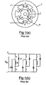
- FIGS 1(a) and 1(b) illustrate a typical 3-phase switched reluctance (SR) machine and a common electronic switching circuit which may be used to control the machine.
- the machine essentially consists of a stator s defining salient stator poles 1, 1', 2, 2', 3, 3' on which are wound phase windings w, of which only one is shown in association with a set of poles 2, 2', and a rotor r with salient poles 4, 4' and 5, 5'.
- this doubly salient machine is quite different in its characteristics and performance from singly salient reluctance machines.
- the latter are generally referred to as synchronous reluctance machines and operate on sinusoidal or quasi-sinusoidal voltage and current waveforms.
- Electronic switching circuits are arranged to supply unidirectional current to the phase windings w.
- each phase winding in the machine of Figure 1(a) is associated with a circuit leg comprising a pair of electronic switches in series with each winding w across a dc supply.
- a description of switched reluctance machines, and their design and control can be found in the paper 'The Characteristics, Design and Applications of Switched Reluctance Motors and Drives' by Dr. J. M. Stephenson et al presented at PCIM '93 Conference and Exhibition at Nurnberg, Germany between 21st and 24th June 1993.
- an SR motor requires a bi-polar excitation voltage applied to the phase winding so as to force the flux in the phase winding up or down as and when required, according to the timing of the control strategy used.
- the flux in a given phase is generally unipolar, the current need not reverse during a phase period. It is commonly accepted that SR machines are conventionally run with unipolar currents.
- phase currents in, for example, a 3-phase SR machine are generally spaced by 120° in respect of their fundamental frequency component, but they do not always sum to zero due to the non-sinusoidal shape caused by their harmonic content. This means that a 3-phase switching circuit for an SR machine cannot necessarily use a conventional star(wye)- or delta-connected inverter by which to derive dc power from an ac source.
- FIG. 1(b) A well-known circuit suitable for switched reluctance machines, which can be operated in several ways, is shown in Figure 1(b).
- first method of operating the circuit both switches t of a leg are switched on and off together so that at switch-off the current transfers from the switches to flow through the diodes d.
- second method only one of the two switches t is opened so that the current circulates or "freewheels", due to the stored magnetic energy associated with the winding through one switch and one diode. Both switches are turned off at the end of a phase conduction period.
- the current in the phase winding is typically controlled by chopping, in which case the machine is said to be 'current fed'.
- Figures 2(a) and (b) illustrate typical chopped motoring and generating phase winding current waveforms, respectively, without freewheeling.
- the current is illustrated in relation to angle ⁇ of rotation of the rotor with respect to the stator.
- phase period defined as the time corresponding to one cycle of phase inductance variation.
- the time rate of change of flux linkage is determined by the voltage applied to the winding, and the rate of change with respect to angle therefore falls as the speed rises.
- Corresponding phase winding currents are illustrated in Figure 3(a) and (b), respectively, for motoring and generating operation. Operation in this manner is called the "single-pulse" mode of operation in which the machine is said to be 'voltage fed'.
- the 'conduction angle' ⁇ c in Figure 3(a) and (b) is the angle over which the switches are closed: ⁇ on is the 'switch-on angle' and ⁇ off is the 'switch-off angle'.
- the flux linkage waveform ⁇ of the phase winding is illustrated by the broken lines. Following closing of the switches t in Figure 1(b) associated with a phase winding, the flux linkage grows linearly. When the switches are opened, the flux linkage falls linearly, the current flowing through the diodes d imposing a voltage of -V s on the windings.
- the circuit of Figure 1(b) is well suited to controlling the current in the inherently inductive windings of an SR machine. Turning both switches on applies the full supply voltage to the winding of a particular leg, forcing the flux (and, therefore, the current) to the required value at the maximum possible rate. Opening both switches then brings the diodes into conduction and forces the flux (and the current) down quickly. Opening only one switch provides a freewheel path for the winding current, with only a small negative winding voltage - flux then falls at only a relatively low rate.
- the winding flux and/or current can be controlled effectively and with relatively low switching losses. Stored energy in the winding (as at the end of a phase period when the switches are turned-off) is returned to the supply via the diodes.
- the circuit of Figure 1(b) is also fault-tolerant. Because the winding is placed between the two switches, there is no possibility of a direct short circuit across the dc supply.
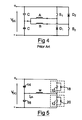
- the second of the above drawbacks can be overcome by using the so-called H circuit shown in Figure 4.
- the switched reluctance machine windings are connected to a common centre point between the two smoothing capacitors C.
- Half the supply voltage is then available for inducing flux growth and half is available for forcing the flux down.
- the inherent operation of the basic H circuit is restricted to voltage (single-pulse) control of an SR machine having an even number of phases. The even number of phases is required because some of the energy drawn from, say, the top smoothing capacitor to the winding of phase A is returned to the lower capacitor at switch off.
- the invention can make use of the half-bridge circuit which is readily available in pre-assembled packages.
- the two switch devices are energised in turn for each excitation of the phase winding to which the circuit is connected.
- the switch devices act as two independent power circuits connected so that they share the switching burden either by being energised alternately or for alternate groups of successive phase excitations.
- one leg of a switching circuit for a reluctance machine comprises first and second power switches 10 and 12.
- the power switches may be any suitable devices, such as bipolar power semi-conductor transistors, power field effect transistors or thyristors.
- One side of the first switch 10 is connected with a positive power supply rail +V DC and the other side of the second switch 12 is connected with a negative power supply rail -V DC .
- the first and second switches are connected together and also to one end of the phase winding w of the reluctance machine to be controlled (see Figure 1(a)).
- the other end of the winding w is connected between a pair of serially connected capacitors 14 and 16.
- the opposite ends of the capacitors are also respectively connected with the first and second power supply rails +V DC and -V DC .
- a diode 18/20 is connected across each of the switches 10/12.
- the pairs of switches and diodes connected as shown in Figure 5 are available in standard electronic component packages as half-bridge modules.
- the broken line boxes in Figure 5 illustrate such an arrangement, where the module contains one switch and one diode.
- Alternative forms are available where all four devices (10, 12, 18 and 20) are contained in one single module. Examples of these are the insulated gate bipolar transistor-based packages MG25Q2YS40 and MG150Q2YS40. manufactured by Toshiba Corporation, Tokyo, Japan. The skilled person will appreciate that other variants exist which will also be suitable in particular applications to equal effect.
- the switches 10 and 12 shown in Figure 5 are typically implemented as insulated gate bipolar transistors, but it will be appreciated by the skilled person that other power switching devices could be used and many are available in the half-bridge module packages referred to. It will also be appreciated that the circuit of Figure 5 is for a single phase winding of a reluctance machine.
- FIG. 10(a) This may be the only phase of the machine or one of a plurality.
- a circuit according to the invention can be connected to each phase, as shown in Figure 10(a) in which like components have been assigned the same reference numerals as in Figure 5 for each of the three phases illustrated.
- FIG 10(b) An alternative form of multiphase circuit is shown in Figure 10(b) in which a pair of capacitors 14' and 16' are connected between the power rails +V DC and -V DC . The common mid-point between the capacitors is connected with one end of each of the windings. It will be apparent to one skilled in the art that any of the capacitors in Figures 5, 10(a) and 10(b) could comprise two or more individual capacitors connected in series or parallel to yield the current and voltage ratings required for any particular application.
- the circuit of Figure 5 uses either the switch/diode pair 10 and 20 or the pair 12 and 18 for a phase cycle of the machine.
- the phase current I ph i.e. the current in the winding
- the current in each switch, I 10 and I 12 indicates that the switches are operated alternately.
- the switch 10 is switched on to be conducting at point A in Figure 6(a) at the start of the conduction period.
- the circuit uses the switch/diode combinations of 10 and 20, or 12 and 18 for each phase period.
- the circuit is, in effect, a pair of power circuits connected together to provide winding excitation current of a polarity which, in the manner described above, alternates on successive phase periods. This alternating duty reduces capacitor voltage swings to a minimum.
- phase currents and voltages are dependent on each other (and in which the phase currents normally sum to zero).
- the current in the phase winding is unidirectional during any one phase period (i.e. it is unipolar).
- the current direction changes as shown in Figures 6(a) and 6(b).
- the frequency of current reversal is therefore a maximum of half the frequency of the electrical cycle. This is in contrast to inverter-fed machines where the frequency of voltage and current reversal is tied exactly to the electrical cycle.
- each phase excitation draws current from (and returns energy to) both capacitors, there should be no long-term drift of the mid-point voltage between the capacitors.
- a resistor or some other means of balancing voltage
- active balancing will be required to monitor the mid-point potential between the capacitors and to modulate the operation of the switches 10 and 12 in some fashion so as to adjust the current drain and hence equalise the voltages across each capacitor.
- the mid-point voltage could be monitored and used to address the SR control circuitry such that additional energy is drawn from the capacitor having the higher voltage to achieve a balance.
- a simple comparator-type circuit, with hysteresis, can be used to indicate an imbalance over a certain threshold. When the threshold is reached the controller addresses one switch continuously until the imbalance has fallen or even been reversed, after which normal alternate duty operation is restored.
- Figure 7 illustrates a hysteresis-based controller for this purpose.
- a positive voltage hysteresis comparator 22 compares a reference voltage +V ref with a feedback signal V fb indicative of the mid-point voltage between the capacitors 14 and 16. When the difference between the two voltage signals exceeds the predetermined threshold, the output from the comparator is applied to a selector switch 24 which switches operational duty from one switch to the other.
- V fb rising in a positive sense above the threshold magnitude will cause the selector 24 to enable energisation of the switch 12. If V fb falls below the negative threshold, the switch 24 will enable energisation of the switch 10.
- the actual timed firing signals are derived from a conventional SR timing control circuit in conventional manner coincident with the beginning and the end of each conduction period. It will be appreciated by the person of ordinary skill that the above operation of the single phase arrangement of Figure 5 applies to each of the phases in the circuits of Figures 10(a) and 10(b) mutatis mutandis.
- the motor may be required to operate in a stalled condition in which it does not produce sufficient torque according to the normal switching sequence.
- the one or more phases connected with the circuit(s) according to this invention can be driven for extended periods by energising either one of the switches. However, this creates an imbalance in the charges on the capacitors 14 and 16. This can be countered by swapping between switch/diode pairs exciting the same phase. The effect of transition between switch/diode pairs will be to cause perturbations in the torque output of the motor at the point of changeover. This is illustrated in Figure 8 in which the phase current I ph swapped between switches is shown. At the transition, the torque output T is disturbed and a sharp drop in torque is created until the inverted phase current I ph according to the change in switch is established.
- the circuit of the invention allows low-cost, readily available half-bridge inverter semi-conductor modules to be used for SR machine control.
- For an n-phase motor it reduces the number of motor phase connections required from 2n (for the conventional circuit) to n+1, with no practical restrictions placed on the value of n.
- the reduction in the number of machine cables may be particularly valuable in applications requiring very long cable runs and, for example, in environmentally sealed motors where additional connections are costly and likely to increase the risk of undermining the integrity of the sealed unit.
- the circuit of the invention can utilise each switch on average for only half the time as the equivalent in a conventional circuit. While this implies an inefficient use of the switches, it also means that the thermal loss per switch and diode pair is halved. Thus, the current capability of each switch is increased (theoretically doubled) or the current rating of each switch for a given application can be reduced.
- applications using transistors as the switches are defined in terms of their peak current handling capability as well as thermal rating. In many applications the peak current consideration will be dominant, so the transistors may be over-sized in terms of thermal load in the circuit of the invention because of this. Nevertheless, this will reduce the heat sinking requirements which may be beneficial in applications in which space is limited.
- Figure 9 illustrates control logic by which transfer between the switches of the circuit may be effected on alternate phases.
- a changeover command on line 30, is applied to the data input of a D-type flip-flop 32 and to one input of a two input AND gate 34.
- the inverted output of the D-type flip-flop is applied to the other input of the AND gate 34.
- the output of the AND gate 34 is applied to the CE input of a J/K-type flip-flop 36 which receives an enabling voltage V DD at the J and K inputs.
- AND gates 38/40 provide the driving signal for each of the switches 10 and 12 of the circuit in Figure 5.
- the non-inverted output from the J/K-type flip-flop 36 is applied to the AND gate 38 and the inverted output of the flip-flop 36 is applied to the AND gate 40.
- a switch driving signal is applied on line 42 to the other input of each of the AND gates.
- the combined action of the flip-flop 36 and the AND gates 38 and 40 is such as to steer the switch driving signal 42 to either of the two outputs 41 and 43 to drive the high-side and low-side switches 10 and 12 respectively.
- the changeover command on line 30 is initiated every time an active phase period has ended following enablement of one of the switches.
- the timed switch driving signal is then available on the output of the AND gate corresponding to the other of the transistors for the next active phase period.
Landscapes
- Engineering & Computer Science (AREA)
- Power Engineering (AREA)
- Control Of Electric Motors In General (AREA)
Abstract
Description
Claims (15)
- A switching circuit for a phase winding of a doubly salient reluctance machine, comprising a pair of switch devices serially connected between a positive and a negative power rail, a pair of capacitors serially connected between the power rails in parallel with the switching devices, and a diode connected across each switch device to conduct towards the positive rail, the phase winding being connectable between the switching devices at one end and between the capacitors at the other end.
- A circuit as claimed in claim 1 in which each switch device comprises a transistor.
- A circuit as claimed in claim 2 in which each transistor is an insulated gate bipolar transistor.
- A circuit as claimed in any of claims 1 to 3 in which each of the switch devices and its associated diode are formed as a preconnected module.
- A circuit as claimed in any of claims 1 to 3 in which the pair of switches and the respectively connected diodes are formed as a preconnected module.
- A switched reluctance machine system comprising: a doubly salient reluctance machine having a rotor, a stator and at least one phase winding; and a switch circuit comprising a pair of switch devices serially connected between a positive and a negative power rail, a pair of capacitors serially connected between the power rails in parallel with the switch devices, and a diode connected across each switch device to conduct towards the positive rail, the phase winding being connected between the switch devices at one end and between the capacitors at the other end, the switch means being selectively actuatable to energise the phase winding such that the frequency of current reversal in the phase winding is not greater than half the frequency of the electrical cycle of the machine.
- A system as claimed in claim 6 in which each of the switch devices is actuated for alternate phase conduction periods.
- A system as claimed in any of claims 6 or 7 in which each switch device comprises a transistor.
- A system as claimed in any of claims 6 to 8 in which each of the switch devices and its associated diode is formed as a preconnected module.
- A system as claimed in any of claims 6 to 8 in which the pair of the switch devices and the respectively connected diodes are formed as a preconnected module.
- A system as claimed in any of claims 6 to 10 including monitoring means responsive to the voltage between the capacitors exceeding a predetermined threshold magnitude while one of the switch devices is actuated to disable the said one device and actuate the other switch device.
- A method of operating a switching circuit for a phase winding of a switched reluctance machine comprising a rotor, a stator and at least one phase winding, which switching circuit comprises a pair of switch devices serially connected between a positive and a negative power rail, a pair of capacitors serially connected between the power rails in parallel with the switch devices, and a diode connected across each switch device to conduct towards the positive rail, the phase winding being connected between the switch devices at one end and between the capacitors at the other end, the method comprising :
actuating the switch devices in turn such that the frequency of current reversal in the phase winding is not greater than half the frequency of the electrical cycle of the machine. - A method as claimed in claim 12 in which each switch device is selected for groups of successive conduction periods of the machine, the switch devices being selected alternatively for successive groups.
- A method as claimed in claim 15 in which the voltage at a mid-point between the capacitors is monitored and one of the switch devices is selected when the mid-point voltage exceeds a threshold.
- A method as claimed in claim 12 in which the switch devices are selected for alternate conduction periods of the same phase.
Applications Claiming Priority (2)
| Application Number | Priority Date | Filing Date | Title |
|---|---|---|---|
| GB9713136 | 1997-06-20 | ||
| GBGB9713136.1A GB9713136D0 (en) | 1997-06-20 | 1997-06-20 | Switching circuit for a reluctance machine |
Publications (3)
| Publication Number | Publication Date |
|---|---|
| EP0886370A2 true EP0886370A2 (en) | 1998-12-23 |
| EP0886370A3 EP0886370A3 (en) | 1999-04-28 |
| EP0886370B1 EP0886370B1 (en) | 2003-12-03 |
Family
ID=10814721
Family Applications (1)
| Application Number | Title | Priority Date | Filing Date |
|---|---|---|---|
| EP98304601A Expired - Lifetime EP0886370B1 (en) | 1997-06-20 | 1998-06-10 | Switching circuit for a reluctance machine |
Country Status (4)
| Country | Link |
|---|---|
| US (1) | US6087799A (en) |
| EP (1) | EP0886370B1 (en) |
| DE (1) | DE69820158T2 (en) |
| GB (1) | GB9713136D0 (en) |
Cited By (5)
| Publication number | Priority date | Publication date | Assignee | Title |
|---|---|---|---|---|
| EP0982845A2 (en) * | 1998-08-28 | 2000-03-01 | Switched Reluctance Drives Limited | Switched reluctance drive with high power factor |
| EP1063761A1 (en) * | 1999-06-22 | 2000-12-27 | The University of Warwick | Power converters for variable reluctance motors |
| US7268516B2 (en) | 2002-09-12 | 2007-09-11 | Switched Reluctance Drivers Limited | Circuit for use with switched reluctance machines |
| US7906931B2 (en) | 2006-12-04 | 2011-03-15 | Switched Reluctance Drives Limited | Control of a switched reluctance machine |
| CN104092343A (en) * | 2014-07-01 | 2014-10-08 | 李佳军 | DC motor with rotary magnetic field |
Families Citing this family (22)
| Publication number | Priority date | Publication date | Assignee | Title |
|---|---|---|---|---|
| DE19826731C2 (en) * | 1998-06-16 | 2000-10-26 | Gruendl & Hoffmann | Half-bridge assembly |
| JP2000347751A (en) * | 1999-06-02 | 2000-12-15 | Aisin Seiki Co Ltd | Chopping conducting device |
| GB9928843D0 (en) * | 1999-12-06 | 2000-02-02 | Lucas Industries Ltd | Switched reluctance generator and a method of controlling such a generator |
| US6388417B1 (en) * | 1999-12-06 | 2002-05-14 | Macrosonix Corporation | High stability dynamic force motor |
| GB0028602D0 (en) * | 2000-11-23 | 2001-01-10 | Switched Reluctance Drives Ltd | Operation of switched reluctance drive systems from dual voltage sources |
| US6528964B2 (en) * | 2001-03-12 | 2003-03-04 | General Motors Corporation | Method and system of reducing turn-off loss and noise in a switched reluctance motor drive |
| US7205736B2 (en) * | 2002-04-24 | 2007-04-17 | Texas Instruments Incorporated | Method for voltage feedback for current mode linear motor driver |
| KR100500244B1 (en) * | 2003-02-07 | 2005-07-11 | 삼성전자주식회사 | Power supply and control method thereof |
| US7352544B2 (en) * | 2005-07-07 | 2008-04-01 | Pratt + Whitney Canada Corp. | Method and apparatus for providing a remedial strategy for an electrical circuit |
| US20070278984A1 (en) * | 2006-05-31 | 2007-12-06 | Rodwan Tarek Adra | 2-Phase switched reluctance device and associated control topologies |
| GB0702975D0 (en) * | 2007-02-15 | 2007-03-28 | Switched Reluctance Drives Ltd | Control of an electrical machine |
| CN100525066C (en) * | 2008-02-02 | 2009-08-05 | 南京航空航天大学 | DC power generation system for two-channel output electric excitation dual protrusion pole motor |
| US9209653B2 (en) | 2010-06-28 | 2015-12-08 | Maxwell Technologies, Inc. | Maximizing life of capacitors in series modules |
| JP5808630B2 (en) * | 2011-09-28 | 2015-11-10 | 株式会社ミツバ | SR motor control device |
| CN102510152A (en) * | 2011-11-24 | 2012-06-20 | 南京航空航天大学 | Hybrid excitation structure of double-salient motor |
| CN102497091A (en) * | 2011-12-26 | 2012-06-13 | 天津清源电动车辆有限责任公司 | Three-phase inverter fault tolerance circuit used for electric vehicle |
| GB2520260B (en) * | 2013-11-12 | 2015-08-19 | Sevcon Ltd | Method and apparatus for control of switched reluctance motors |
| US10693348B2 (en) * | 2016-05-23 | 2020-06-23 | Reginald Garcia | Enhanced efficiency motor and drive circuit |
| RU2658654C2 (en) * | 2016-12-13 | 2018-06-22 | Общество с ограниченной ответственностью Научно-производственное предприятие "Донские технологии" | Method of sensorless control of linear reciprocating valve-inductor pair-phase generator |
| RU2662233C1 (en) * | 2017-11-22 | 2018-07-25 | Общество с ограниченной ответственностью Научно-производственное предприятие "Резонанс" (ООО НПП "Резонанс") | Induction electrical machine |
| RU2694364C1 (en) * | 2018-11-13 | 2019-07-12 | Общество с ограниченной ответственностью "Смартер" | Method for control of inductor machine |
| CN117277908A (en) * | 2023-11-21 | 2023-12-22 | 佳沃德(佛山)科技有限公司 | Power converter of high-speed switch reluctance motor |
Citations (3)
| Publication number | Priority date | Publication date | Assignee | Title |
|---|---|---|---|---|
| EP0074752A1 (en) * | 1981-09-08 | 1983-03-23 | TASC Drives Limited | Power conversion circuit |
| EP0455869A2 (en) * | 1990-05-05 | 1991-11-13 | Heraeus Sepatech GmbH | Circuit arrangement for driving a centrifuge |
| DE4416342C1 (en) * | 1994-05-09 | 1995-05-11 | Hans Hermann Rottmerhusen | Electronics for commutator motors |
Family Cites Families (16)
| Publication number | Priority date | Publication date | Assignee | Title |
|---|---|---|---|---|
| DE3022836C1 (en) * | 1980-06-19 | 1981-10-29 | Papst-Motoren Kg, 7742 St Georgen | Brushless DC motor |
| EP0178615A3 (en) * | 1984-10-19 | 1987-08-05 | Kollmorgen Corporation | Power supply systems for inductive elements |
| EP1492220A3 (en) * | 1991-09-20 | 2005-03-09 | Hitachi, Ltd. | IGBT-module |
| IN186007B (en) * | 1991-12-10 | 2001-06-02 | British Tech Group | |
| US5233509A (en) * | 1992-04-03 | 1993-08-03 | International Business Machines Corporation | Switch-mode AC-to-DC converter |
| US5825112A (en) * | 1992-08-06 | 1998-10-20 | Electric Power Research Institute, Inc. | Doubly salient motor with stationary permanent magnets |
| US5304882A (en) * | 1992-05-11 | 1994-04-19 | Electric Power Research Institute, Inc. | Variable reluctance motors with permanent magnet excitation |
| GB9311176D0 (en) * | 1993-05-29 | 1993-07-14 | Univ Warwick | Electric motor drive |
| GB9414116D0 (en) * | 1994-07-13 | 1994-08-31 | Switched Reluctance Drives Ltd | Polyphase switched reluctance machines |
| US5578911A (en) * | 1994-09-21 | 1996-11-26 | Chrysler Corporation | Method and apparatus for power regeneration in an electric vehicle motor drive using a deadtime generator and having continuously variable regeneration control |
| US5576943A (en) * | 1995-05-22 | 1996-11-19 | Kaman Electromagnetics Corporation | Soft switched three phase inverter with staggered resonant recovery system |
| GB9513916D0 (en) * | 1995-07-07 | 1995-09-06 | Switched Reluctance Drives Ltd | Switching circuit for an inductive load |
| US5742139A (en) * | 1996-07-26 | 1998-04-21 | Dana Corporation | Method and apparatus for reducing noise in a variable reluctance motor |
| US5739662A (en) * | 1996-08-30 | 1998-04-14 | Emerson Electric Co. | Low cost drive for a reluctance machine having fully-pitched windings |
| US5929590A (en) * | 1997-01-07 | 1999-07-27 | Emerson Electric Co. | Method and apparatus for implementing sensorless control of a switched reluctance machine |
| US5936373A (en) * | 1997-09-26 | 1999-08-10 | Emerson Electric Co. | Wide pole switched reluctance machine and method of its control |
-
1997
- 1997-06-20 GB GBGB9713136.1A patent/GB9713136D0/en active Pending
-
1998
- 1998-06-10 DE DE69820158T patent/DE69820158T2/en not_active Expired - Lifetime
- 1998-06-10 EP EP98304601A patent/EP0886370B1/en not_active Expired - Lifetime
- 1998-06-19 US US09/100,280 patent/US6087799A/en not_active Expired - Lifetime
Patent Citations (3)
| Publication number | Priority date | Publication date | Assignee | Title |
|---|---|---|---|---|
| EP0074752A1 (en) * | 1981-09-08 | 1983-03-23 | TASC Drives Limited | Power conversion circuit |
| EP0455869A2 (en) * | 1990-05-05 | 1991-11-13 | Heraeus Sepatech GmbH | Circuit arrangement for driving a centrifuge |
| DE4416342C1 (en) * | 1994-05-09 | 1995-05-11 | Hans Hermann Rottmerhusen | Electronics for commutator motors |
Non-Patent Citations (1)
| Title |
|---|
| BARNES M ET AL: "TWO PHASE SWITCHED RELUCTANCE DRIVE WITH NEW POWER ELECTRONIC CONVERTER FOR LOW COST APPLICATIONS" EPE '95: 6TH. EUROPEAN CONFERENCE ON POWER ELECTRONICS AND APPLICATIONS, SEVILLA, SEPT. 19 - 21, 1995, vol. & 1, no. CONF. 6, 19 September 1995, pages 1.427-1.430, XP000537561 EUROPEAN POWER ELECTRONICS AND DRIVES ASSOCIATION * |
Cited By (8)
| Publication number | Priority date | Publication date | Assignee | Title |
|---|---|---|---|---|
| EP0982845A2 (en) * | 1998-08-28 | 2000-03-01 | Switched Reluctance Drives Limited | Switched reluctance drive with high power factor |
| EP0982845B1 (en) * | 1998-08-28 | 2011-09-28 | Nidec SR Drives Ltd. | Switched reluctance drive with high power factor |
| EP1063761A1 (en) * | 1999-06-22 | 2000-12-27 | The University of Warwick | Power converters for variable reluctance motors |
| US6384564B1 (en) | 1999-06-22 | 2002-05-07 | University Of Warwick | Electrical machines |
| US7268516B2 (en) | 2002-09-12 | 2007-09-11 | Switched Reluctance Drivers Limited | Circuit for use with switched reluctance machines |
| US7906931B2 (en) | 2006-12-04 | 2011-03-15 | Switched Reluctance Drives Limited | Control of a switched reluctance machine |
| EP1931025A3 (en) * | 2006-12-04 | 2015-10-07 | Nidec SR Drives Ltd. | Control of a switched reluctance machine |
| CN104092343A (en) * | 2014-07-01 | 2014-10-08 | 李佳军 | DC motor with rotary magnetic field |
Also Published As
| Publication number | Publication date |
|---|---|
| EP0886370A3 (en) | 1999-04-28 |
| EP0886370B1 (en) | 2003-12-03 |
| US6087799A (en) | 2000-07-11 |
| DE69820158D1 (en) | 2004-01-15 |
| DE69820158T2 (en) | 2004-11-25 |
| GB9713136D0 (en) | 1997-08-27 |
Similar Documents
| Publication | Publication Date | Title |
|---|---|---|
| EP0886370B1 (en) | Switching circuit for a reluctance machine | |
| US6140729A (en) | Electrical machines | |
| US5304882A (en) | Variable reluctance motors with permanent magnet excitation | |
| US5811905A (en) | Doubly-fed switched reluctance machine | |
| US5929590A (en) | Method and apparatus for implementing sensorless control of a switched reluctance machine | |
| AU619096B2 (en) | Current chopping strategy for switched reluctance machines | |
| EP1208643B1 (en) | Control of an electrical reluctance machine | |
| US5387854A (en) | Method of torque notch minimization for quasi square wave back EMF permanent magnet synchronous machines with voltage source drive | |
| Pollock et al. | A unipolar converter for a switched reluctance motor | |
| US5173651A (en) | Electrical drive systems | |
| US5166591A (en) | Current chopping strategy for generating action in switched reluctance machines | |
| US5689164A (en) | Resonant power electronic control of switched reluctance motor | |
| EP0802623B1 (en) | Converter circuit for a polyphase switched inductive load | |
| US6384564B1 (en) | Electrical machines | |
| KR100600540B1 (en) | Operation of switched reluctance machines | |
| US6661206B2 (en) | Soft chopping for switched reluctance generators | |
| US6137256A (en) | Soft turn-off controller for switched reluctance machines | |
| EP0910887A1 (en) | Reluctance machine with fractional pitch winding and drive therefor | |
| US6642683B1 (en) | Controller and associated drive assembly for power sharing, time sliced control of a brushless direct current motor | |
| US7471055B2 (en) | Controller, drive assembly and half-bridge assembly for providing a voltage | |
| US6661190B1 (en) | Controller and associated drive assembly controlling a brushless direct current motor | |
| US5847532A (en) | Switching circuit for an inductive load | |
| US6906481B1 (en) | Power sharing high frequency motor drive modular system | |
| Somsiri et al. | Three-phase full-bridge converters applied to switched reluctance motor drives with a modified switching strategy | |
| Dahmane et al. | A novel boost capacitor circuit to enhance the performance of the switched reluctance motor |
Legal Events
| Date | Code | Title | Description |
|---|---|---|---|
| PUAI | Public reference made under article 153(3) epc to a published international application that has entered the european phase |
Free format text: ORIGINAL CODE: 0009012 |
|
| AK | Designated contracting states |
Kind code of ref document: A2 Designated state(s): DE FR GB IT |
|
| AX | Request for extension of the european patent |
Free format text: AL;LT;LV;MK;RO;SI |
|
| PUAL | Search report despatched |
Free format text: ORIGINAL CODE: 0009013 |
|
| AK | Designated contracting states |
Kind code of ref document: A3 Designated state(s): AT BE CH CY DE DK ES FI FR GB GR IE IT LI LU MC NL PT SE |
|
| AX | Request for extension of the european patent |
Free format text: AL;LT;LV;MK;RO;SI |
|
| 17P | Request for examination filed |
Effective date: 19990916 |
|
| AKX | Designation fees paid |
Free format text: DE FR GB IT |
|
| GRAG | Despatch of communication of intention to grant |
Free format text: ORIGINAL CODE: EPIDOS AGRA |
|
| 17Q | First examination report despatched |
Effective date: 20011106 |
|
| GRAG | Despatch of communication of intention to grant |
Free format text: ORIGINAL CODE: EPIDOS AGRA |
|
| GRAG | Despatch of communication of intention to grant |
Free format text: ORIGINAL CODE: EPIDOS AGRA |
|
| GRAH | Despatch of communication of intention to grant a patent |
Free format text: ORIGINAL CODE: EPIDOS IGRA |
|
| GRAH | Despatch of communication of intention to grant a patent |
Free format text: ORIGINAL CODE: EPIDOS IGRA |
|
| GRAO | Approval/disapproval following communication of intention to grant |
Free format text: ORIGINAL CODE: EPIDOSNAGR3 |
|
| GRAU | Approval following communication of intention to grant |
Free format text: ORIGINAL CODE: EPIDOSNAGR4 |
|
| GRAA | (expected) grant |
Free format text: ORIGINAL CODE: 0009210 |
|
| AK | Designated contracting states |
Kind code of ref document: B1 Designated state(s): DE FR GB IT |
|
| REG | Reference to a national code |
Ref country code: GB Ref legal event code: FG4D |
|
| REF | Corresponds to: |
Ref document number: 69820158 Country of ref document: DE Date of ref document: 20040115 Kind code of ref document: P |
|
| ET | Fr: translation filed | ||
| PLBE | No opposition filed within time limit |
Free format text: ORIGINAL CODE: 0009261 |
|
| STAA | Information on the status of an ep patent application or granted ep patent |
Free format text: STATUS: NO OPPOSITION FILED WITHIN TIME LIMIT |
|
| 26N | No opposition filed |
Effective date: 20040906 |
|
| PGFP | Annual fee paid to national office [announced via postgrant information from national office to epo] |
Ref country code: IT Payment date: 20090617 Year of fee payment: 12 |
|
| PG25 | Lapsed in a contracting state [announced via postgrant information from national office to epo] |
Ref country code: IT Free format text: LAPSE BECAUSE OF NON-PAYMENT OF DUE FEES Effective date: 20100610 |
|
| REG | Reference to a national code |
Ref country code: FR Ref legal event code: CD |
|
| REG | Reference to a national code |
Ref country code: DE Ref legal event code: R082 Ref document number: 69820158 Country of ref document: DE Representative=s name: UEXKUELL & STOLBERG, DE |
|
| REG | Reference to a national code |
Ref country code: DE Ref legal event code: R082 Ref document number: 69820158 Country of ref document: DE Representative=s name: UEXKUELL & STOLBERG PARTNERSCHAFT VON PATENT- , DE Effective date: 20121217 Ref country code: DE Ref legal event code: R082 Ref document number: 69820158 Country of ref document: DE Representative=s name: UEXKUELL & STOLBERG, DE Effective date: 20121217 Ref country code: DE Ref legal event code: R081 Ref document number: 69820158 Country of ref document: DE Owner name: NIDEC SR DRIVES LTD., HARROGATE, GB Free format text: FORMER OWNER: SWITCHED RELUCTANCE DRIVES LTD., HARROGATE, NORTH YORKSHIRE, GB Effective date: 20121217 Ref country code: DE Ref legal event code: R081 Ref document number: 69820158 Country of ref document: DE Owner name: NIDEC SR DRIVES LTD., GB Free format text: FORMER OWNER: SWITCHED RELUCTANCE DRIVES LTD., HARROGATE, GB Effective date: 20121217 |
|
| REG | Reference to a national code |
Ref country code: FR Ref legal event code: PLFP Year of fee payment: 18 |
|
| PGFP | Annual fee paid to national office [announced via postgrant information from national office to epo] |
Ref country code: DE Payment date: 20150626 Year of fee payment: 18 |
|
| PGFP | Annual fee paid to national office [announced via postgrant information from national office to epo] |
Ref country code: FR Payment date: 20150617 Year of fee payment: 18 |
|
| REG | Reference to a national code |
Ref country code: DE Ref legal event code: R119 Ref document number: 69820158 Country of ref document: DE |
|
| REG | Reference to a national code |
Ref country code: FR Ref legal event code: ST Effective date: 20170228 |
|
| PG25 | Lapsed in a contracting state [announced via postgrant information from national office to epo] |
Ref country code: FR Free format text: LAPSE BECAUSE OF NON-PAYMENT OF DUE FEES Effective date: 20160630 Ref country code: DE Free format text: LAPSE BECAUSE OF NON-PAYMENT OF DUE FEES Effective date: 20170103 |
|
| PGFP | Annual fee paid to national office [announced via postgrant information from national office to epo] |
Ref country code: GB Payment date: 20170605 Year of fee payment: 20 |
|
| REG | Reference to a national code |
Ref country code: GB Ref legal event code: PE20 Expiry date: 20180609 |
|
| PG25 | Lapsed in a contracting state [announced via postgrant information from national office to epo] |
Ref country code: GB Free format text: LAPSE BECAUSE OF EXPIRATION OF PROTECTION Effective date: 20180609 |