EP0883178A2 - Cryogenic electronic assembly - Google Patents
Cryogenic electronic assembly Download PDFInfo
- Publication number
- EP0883178A2 EP0883178A2 EP98304384A EP98304384A EP0883178A2 EP 0883178 A2 EP0883178 A2 EP 0883178A2 EP 98304384 A EP98304384 A EP 98304384A EP 98304384 A EP98304384 A EP 98304384A EP 0883178 A2 EP0883178 A2 EP 0883178A2
- Authority
- EP
- European Patent Office
- Prior art keywords
- housing
- assembly
- substrate
- adjuster
- circuit
- Prior art date
- Legal status (The legal status is an assumption and is not a legal conclusion. Google has not performed a legal analysis and makes no representation as to the accuracy of the status listed.)
- Withdrawn
Links
Images


Classifications
-
- H—ELECTRICITY
- H01—ELECTRIC ELEMENTS
- H01P—WAVEGUIDES; RESONATORS, LINES, OR OTHER DEVICES OF THE WAVEGUIDE TYPE
- H01P1/00—Auxiliary devices
- H01P1/30—Auxiliary devices for compensation of, or protection against, temperature or moisture effects ; for improving power handling capability
-
- H10W40/305—
-
- H10W72/5363—
-
- H10W72/5522—
-
- H10W72/5524—
Definitions
- This invention relates to electronic assemblies. It particularly relates to assemblies operating at cryogenic temperatures.
- a known technique of operating electronic components at cryogenic temperatures is to mount the components on a so-called "cold finger" within an evacuated chamber.
- a problem can arise in making electrical connections between the exterior of the enclosure, which may be at ambient temperature, and the electronic components, which are at cryogenic temperatures, in that electrically conductive signal paths also provide thermally conductive paths.
- the more connecting paths the greater the conducted heat and the heavier the loading on the cryogenic cooler.
- This is a particular problem with radio-frequency signal paths where conductor dimensions are determined by the need to maintain a good impedance match and may involve the provision of a conducting ground plane.
- the coupling paths also need to allow for the thermal expansion and contraction which may arise due to the thermally-produced movement between the components and the enclosure which occurs when the assembly is being brought to its cryogenic operating temperature or returns to ambient temperature when the apparatus is shut down.
- each path comprises a length of coaxial cable extending between the walls of the enclosure and the cryogenic components.
- this known arrangement suffers the disadvantage that, in order to minimise heat loss by conduction, the cable must be made relatively long. While this arrangement has proved satisfactory where a small number of signal paths is concerned, for large numbers of paths, the large number of parallel paths provides a correspondingly reduced thermal resistance, leading to a proportional increase in heat load.
- coaxial cable will inevitably contain a certain amount of trapped gas which will progressively leak into the vacuum space over a period of time. This gas will provide another mechanism for heat transfer by convection or conduction between ambient and the cold component. The longer the cable, the greater the potential for out gassing of trapped gases. The user then has the inconvenience of having to periodically re-pump the enclosure to restore vacuum.
- the present invention seeks to ameliorate the above disadvantages of the prior art.
- a circuit assembly comprising a first substrate having a first stripline conductor arranged on a first surface thereof and having an end terminating at an edge of the first substrate, a second substrate having a second stripline conductor arranged on a first surface thereof and having an end terminating at an edge of the second substrate, means to align the first and second substrates with their edges spaced apart with the respective ends of the striplines aligned, respective first and second wire links extending between respective longitudinal edges of the end of the first stripline conductor and corresponding edges of the end of the second stripline conductor.
- apparatus for adjusting a circuit operated at cryogenic temperatures comprising an evacuable housing, and means for mounting a circuit to be adjusted within the evacuable housing, the apparatus comprising a cover for the housing arranged to be hermetically sealed to the housing, the cover comprising at least one adjuster disposed in a through bore in the cover, the bore having seal means arranged to cooperate with the adjuster and provide a hermetic seal therewith while allowing movement of the adjuster relative to the cover, the other end of the adjuster being arranged to cooperate with an adjustable member of the circuit whereby the circuit can be adjusted from the exterior of the housing when the interior of the housing is evacuated.
- stripline refers to transmission lines in which at least one conductor comprises a planar conductive member arranged on a substrate. It includes but is not limited to, microstrip and stripline configurations and balanced and unbalanced configurations.
- a cold finger 100 forms part of a cooling engine which in the present embodiment is capable of attaining a temperature in the order of 60K.
- the cold finger 100 terminates in a cold platform 102 on which is mounted an assembly 200 comprising a number of electronic circuit modules.
- the assembly 200 is of double-sided construction.
- the upper surface has three channels comprising sub-assemblies 80, 81; 82, 83; and 84, 85 respectively.
- Module 80 is provided with tuning screws 810, 820 for tuning purposes. For clarity, only two tuning screws have been shown. In practice any number of tuning screws may be provided according to circuit requirements.
- Modules 82, 84 have corresponding screws but these have been omitted for clarity.
- the lower surface has three further channels of which only 82', 83' are shown in Figure 2.
- the cold finger 100, 102 and circuit assembly 200 are surrounded by an enclosure defined by a lower portion 104, an annular intermediate portion 107, and top portion 110.
- Intermediate portion 107 carries electrical connectors and will be referred to as the connector ring.
- an adjustment assembly 600 shown in phantom on Figure 1, may be temporarily utilised in place of top portion 110 to facilitate adjustment while maintaining a vacuum.
- Respective lateral portions 106, 108 connector ring 107 carry the respective input and output connectors for radio-frequency signals and other supply and sensor circuits.
- the radio frequency connectors comprise "K" connectors, but any suitable type may of course be used.
- Input connectors 10, 12, 14 provide inputs to the upper modules 80, 82, 84.
- Input connectors 20, 22, 24 comprise connections to the lower modules, not shown.
- Output signals from output stages 81, 83, 85 appear at output connectors 30, 32, 34 respectively.
- Output signals from the corresponding output stages on the lower surface appear at connectors 40, 42, 44.
- the input signal path from the input connectors 10, 12, 14, to their respective modules 80, 82, 84 are via respective strip line transmission lines 60, 62, 64 on a substrate 66. Corresponding transmission lines, not shown, provide paths to the lower modules. Similarly the output signal paths from output stages 81, 83, 85 are via strip transmission lines 70, 72, 74 on substrate 76. The corresponding strip transmission lines for the lower modules are not shown for clarity.
- the input substrate 66 and output substrate 76 are mounted on the respective lateral walls 106, 108. Feedthrough members 50 provide DC bias connections via respective conductive tracks 52. Respective gaps 700, 710 provide respective thermal breaks between the substrates 66, 76 and the assembly 200 at cryogenic temperature.
- a substrate 66 has an input transmission strip line 62 on first surface.
- the other surface carries a ground plane 68.
- a substrate 800 has an input strip line 822 on its first surface and a ground plane 808 on its opposite surface.
- the substrates are spaced apart by a vacuum space 700 providing a thermal break.
- Electrical connection between the strip lines 62, 822 are by way of a pair of thin wire links 310, 312 arranged adjacent opposite edges of the strip lines 62, 822.
- the links 310, 312 are arranged close to the edges of the strip lines 62, 822.
- the first substrate 66 has first and second pads 302, 304 arranged on its upper surface on either side of the strip line 62. Connection between the ground plane 68 and the pads 302, 304 are via through-plated holes 306. Corresponding pads 804, 802 are provided on the other substrate 800 with corresponding through-plated holes 806. A plurality of links 314, 316, 318, 320 provide the necessary ground plane connections. It will be seen that, as compared with the relatively large cross-section of a coaxial cable, in accordance with the present invention the thermal path is that of a relatively thin wire links 310-320. The present embodiment utilises wire of about 25 ⁇ m diameter as used in bonding integrated circuits and thick-film circuit assemblies.
- any conventional bold wire such as Aluminium or Gold, may be used.
- wire of a metal having a relatively poor thermal conductivity may be employed.
- the choice of such a metal will be determined by metallurgical factors such as compatibility with the metal used for the stripline conductors, as well as thermal properties.
- an adjustment assembly is provided which seals the vacuum enclosure yet which allows the adjusting screws to be adjusted.
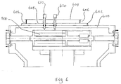
- a module 800 has adjusting screws 810, 820.
- the arrangement shown in Figure 6 and 7 has a first member 600 partially overlain by a second member 602.
- First and second spring-loaded screwdrivers 610, 620 run in respective bores in members 600, 602. These bores have seals 608 which allow axial and rotational movement of screwdrivers 610, 620 while maintaining an adequate vacuum tight seal.
- the screwdrivers 610, 620 are urged outwardly of the enclosure by springs to counter balance the vacuum force which would tend to urge the screwdrivers into the interior of the chamber and to cause the thermally conductive screwdrivers to disengage from their associated adjustment screws when adjustment is not being carried out.
- the upper ends of the screwdrivers terminate in respective enlarged heads which provide a bearing surface for the springs.
- a further plate 604 is provided spaced apart from the upper surface of member 602 by spaces 606.
- the screwdrivers 610, 620 run through bores in plate 604 with a clearance which allows passage of the shaft but does not allow passage of the heads. This limits the extent to which the screwdrivers may enter into the interior of the vacuum chamber.
- the engagement of a screwdriver with an adjusting screw provides a path for heat conduction leading to heat loss from the enclosure and a rise in temperature of the component being adjusted. Allowing the screwdrivers to engage the tuning screws only for the brief time during which adjustments are actually being made minimises the rise in temperature of the circuit being adjusted due to conduction along the screwdriver shaft, and allows the circuit to quickly return to its operating temperature after adjustment.
- the seals do not provide a perfect long-term vacuum seal, they are adequate to maintain a sufficiently good vacuum to allow adjustment to be carried out.
- the cover 600 and its associated components can be removed and replaced by a conventional cover 110. If necessary, the enclosure may be pumped while adjustments are being made to remove any air which may leak past the seals.
- the reduction in heat loss afforded by the present invention may enable the cold finger 100 to adequately cool more than one circuit 200.
- the arrangement shown in Figure 2 is modified by the provision of a further circuit assembly 202 mounted on the first circuit assembly 200.
- the further circuit assembly 202 is provided with a further side walls 106', 108'.
- the closure member 110 is attached to these further side walls. It can be seen that the circuit capacity has been doubled for a relatively small increase in volume.
- circuits 200, 202 comprise modules such as module 800 of figures 6 and 7 which require adjustment
- initially only circuit 200 is mounted on the cold finger together with sidewalls 106, 108.
- a temporary cover is fitted as described with reference to figures 6 and 7 and adjustments made.
- the temporary cover is removed, the second circuit 202 and sidewalls 106', 108' are fitted, and the temporary cover is replaced.
- the adjustable module of the second circuit 202' is then adjusted.
- the temporary cover is removed and the closure member 100 fitted.
- each adjustable module is adjusted using a temporary cover as described above before fitting the next circuit.
- circuit assemblies need not compromise a plurality of identical channels.
- Each channel may consist of a "building block" performing a different function, for example amplification, oscillation, mixing and filtering.
- interconnections between the different building blocks may be made via the exterior of the housing. This allows the signals to be monitored, and individual blocks to be tested, from the outside of the enclosure. However, this is not essential, and some or all of the interconnections may be made within the enclosure.
- one or more intermediate links may be provided between the outer links. This may further reduce the impedance discontinuity presented by the links at the expense of further heat loss.
- metal encompasses alloys.
- substrate encompasses any material suitable for use with microwave and/or Radio frequency applications, and encompasses semiconductors as well as insulators.
Landscapes
- Containers, Films, And Cooling For Superconductive Devices (AREA)
- Cooling Or The Like Of Semiconductors Or Solid State Devices (AREA)
- Cooling Or The Like Of Electrical Apparatus (AREA)
Abstract
Description
Claims (18)
- A circuit assembly comprising a first substrate having a first stripline conductor arranged on a first surface thereof and having an end terminating at an edge of the first substrate, a second substrate having a second stripline conductor arranged on a first surface thereof and having an end terminating at an edge of the second substrate,
means to align the first and second substrates with their edges spaced apart with the respective ends of the striplines aligned, and
respective first and second wire links extending between respective longitudinal edges of the end of the first stripline conductor and corresponding edges of the end of the second stripline conductor. - An assembly as claimed in claim 1 comprising at least one further wire link arranged intermediate the first and second links.
- An assembly as claimed in claim 1 or 2 in which the first and second substrates comprise respective first and second ground planes arranged on respective second surfaces thereof, the first and second ground planes being electrically connected by a plurality of further wire links.
- An assembly as claimed in claim 3 comprising at least one respective ground pad arranged on the respective first surfaces of the first and second substrates, the ground pads being electrically connected to the respective ground planes on the respective second surfaces,
in which the plurality of further wire links extend between the respective ground pads. - An assembly as claimed in any preceding claim in which at least one wire link comprises a metal having a relatively poor thermal conductivity.
- An assembly as claimed in any preceding claim in which the stripline comprises a coplanar waveguide.
- An assembly as claimed in any preceding claim comprising means to maintain the second substrate at a lower temperature than the first substrate.
- An assembly as claimed in claim 7 in which the lower temperature is a cryogenic temperature.
- A hermetic assembly comprising a hermetically-sealed housing and an assembly as claimed in claim 7 or 8 arranged within the housing, in which the first substrate is secured to a wall of the housing, the means to maintain the second substrate are arranged within the housing, and the interior of the housing is evacuated.
- A hermetic assembly as claimed in Claim 9 in which the means to maintain the second substrate comprises a cold finger.
- A hermetic assembly as claimed in claim 10 comprising a further assembly as claimed in any one of claims 1-6 and comprising further first and second substrates, in which the further substrate is secured to the wall of the housing and the further second substrate is mounted on the second substrate.
- A hermetic assembly as claimed in claim 11 comprising at least one still further assembly as claimed in any one of claims 1-6 and comprising at least one still further first and second substrates, in which the or each still further first substrate is secured to the wall of the housing and the or each at least still further second substrate is mounted on the further second substrate.
- Apparatus for adjusting a circuit operated at cryogenic temperatures comprising an evacuable housing, and means for mounting a circuit to be adjusted within the evacuable housing,
the apparatus comprising a cover for the housing arranged to be hermetically sealed to the housing, the cover comprising at least one adjuster disposed in a through bore in the cover, the bore having seal means arranged to cooperate with the adjuster and provide a hermetic seal therewith while allowing movement of the adjuster relative to the cover, the other end of the adjuster being arranged to cooperate with an adjustable member of the circuit whereby the circuit can be adjusted from the exterior of the housing when the interior of the housing is evacuated. - Apparatus as claimed in claim 13 comprising spring means arranged to cooperate with the adjuster to urge the adjuster outwards of the enclosure.
- Apparatus as claimed in claim 13 or 14 comprising means to limit the inward movement of the adjuster.
- Apparatus as claimed in claim 14 in which the adjuster has an enlarged portion at its outwardly remote end, further comprising a plate arranged above the outer surface of the cover and spaced apart therefrom, the adjuster extending through an aperture in the plate with its enlarged portion outwardly of the plate such that inward movement of the adjuster is limited by engagement of the enlarged portion with the plate.
- A method of manufacturing an adjustable circuit assembly comprising an adjustable circuit module arranged within an evacuated housing, the method comprising the steps of:closing the housing using an apparatus as claimed in any one of claims 13-16;adjusting the module; andreplacing the said apparatus with a permanent cover on completion of adjustment.
- A method of manufacturing a circuit assembly comprising a plurality of adjustable circuit modules stacked on top of each other in an evacuated housing, the method comprising the steps of:mounting a first module within the housing;closing the housing with an apparatus as claimed in any one of claims 13-16;adjusting the first module;removing the said apparatus;mounting a further module on top of the first module;refitting the said apparatus;adjusting the further module using the said apparatus; andreplacing the said apparatus with a closure member after completion of adjustment.
Applications Claiming Priority (2)
| Application Number | Priority Date | Filing Date | Title |
|---|---|---|---|
| GB9711379A GB2326029A (en) | 1997-06-03 | 1997-06-03 | Cryogenic electronic assembly with stripline connection and adjustment means |
| GB9711379 | 1997-06-03 |
Publications (2)
| Publication Number | Publication Date |
|---|---|
| EP0883178A2 true EP0883178A2 (en) | 1998-12-09 |
| EP0883178A3 EP0883178A3 (en) | 2000-07-26 |
Family
ID=10813450
Family Applications (1)
| Application Number | Title | Priority Date | Filing Date |
|---|---|---|---|
| EP98304384A Withdrawn EP0883178A3 (en) | 1997-06-03 | 1998-06-03 | Cryogenic electronic assembly |
Country Status (3)
| Country | Link |
|---|---|
| US (1) | US6184757B1 (en) |
| EP (1) | EP0883178A3 (en) |
| GB (1) | GB2326029A (en) |
Cited By (6)
| Publication number | Priority date | Publication date | Assignee | Title |
|---|---|---|---|---|
| EP1253602A4 (en) * | 2000-01-31 | 2003-04-09 | Fujitsu Ltd | THERMALLY INSULATED SIGNAL TRANSMISSION UNIT AND SUPERCONDUCTIVE SIGNAL TRANSMISSION DEVICE |
| US10229864B1 (en) | 2017-09-14 | 2019-03-12 | Northrop Grumman Systems Corporation | Cryogenic integrated circuit having a heat sink coupled to separate ground planes through differently sized thermal vias |
| WO2019089139A1 (en) * | 2017-10-31 | 2019-05-09 | Northrop Grumman Systems Corporation | Thermally isolated ground planes with a superconducting electrical coupler |
| US10290676B2 (en) | 2017-08-15 | 2019-05-14 | Northrop Grumman Systems Corporation | Superconducting device with thermally conductive heat sink |
| US11522118B2 (en) | 2020-01-09 | 2022-12-06 | Northrop Grumman Systems Corporation | Superconductor structure with normal metal connection to a resistor and method of making the same |
| US12027437B2 (en) | 2018-12-20 | 2024-07-02 | Northrop Grumman Systems Corporation | Superconducting device having a plurality of thermal sink layers and a plurality of ground planes |
Families Citing this family (4)
| Publication number | Priority date | Publication date | Assignee | Title |
|---|---|---|---|---|
| FR2801381B1 (en) * | 1999-11-18 | 2002-01-04 | Instrumentation Scient De Labo | DEVICE FOR REFRIGERATING CELLS CONTAINING LIQUID SAMPLES IN PARTICULAR SAMPLES OF PETROLEUM PRODUCTS TO BE ANALYZED |
| FR2856522B1 (en) * | 2003-06-20 | 2005-08-19 | Sagem | COOLED PHOTODETECTOR |
| US8841764B2 (en) * | 2012-01-31 | 2014-09-23 | International Business Machines Corporation | Superconducting quantum circuit having a resonant cavity thermalized with metal components |
| US9612044B2 (en) * | 2012-09-13 | 2017-04-04 | Raytheon Company | Cryocooler having variable-length inertance channel for tuning resonance of pulse tube |
Family Cites Families (15)
| Publication number | Priority date | Publication date | Assignee | Title |
|---|---|---|---|---|
| IT1209844B (en) * | 1981-02-09 | 1989-08-30 | Selenia Ind Elettroniche | DEVICE FOR INFRARED DETECTION OF MANY ELEMENTS WITH HIGH DENSITY OF LOW PASSES FOR THERMAL FINGERS |
| US4761681A (en) * | 1982-09-08 | 1988-08-02 | Texas Instruments Incorporated | Method for fabricating a semiconductor contact and interconnect structure using orientation dependent etching and thermomigration |
| US4686492A (en) * | 1985-03-04 | 1987-08-11 | Tektronix, Inc. | Impedance match connection using multiple layers of bond wires |
| US4739633A (en) * | 1985-11-12 | 1988-04-26 | Hypres, Inc. | Room temperature to cryogenic electrical interface |
| US4870375A (en) * | 1987-11-27 | 1989-09-26 | General Electric Company | Disconnectable microstrip to stripline transition |
| FR2638023B1 (en) | 1988-10-13 | 1992-07-31 | Telecommunications Sa | CRYOSTATIC DEVICE FOR RADIATION DETECTOR |
| FR2646559B1 (en) * | 1989-04-28 | 1991-07-05 | Commissariat Energie Atomique | MEASURING SYSTEM CONSISTING OF A RADIATION DETECTION CIRCUIT, A READING CIRCUIT AND A MEDIUM SUCH AS A COLD CRYOSTAT FINGER |
| FR2651315B1 (en) * | 1989-08-22 | 1991-11-15 | Detecteurs Infra Rouges Ste Fs | INFRARED DETECTION DEVICE. |
| US5518674A (en) * | 1991-06-28 | 1996-05-21 | Texas Instruments Incorporated | Method of forming thin film flexible interconnect for infrared detectors |
| DE69107082T2 (en) * | 1991-11-16 | 1995-05-24 | Hewlett Packard Gmbh | A connector assembly for detachable connection between two conductor strips. |
| JPH0637202A (en) * | 1992-07-20 | 1994-02-10 | Mitsubishi Electric Corp | Microwave IC package |
| JP2953273B2 (en) * | 1993-10-22 | 1999-09-27 | 住友電気工業株式会社 | How to connect devices that cool to low temperatures |
| US5543662A (en) | 1994-09-20 | 1996-08-06 | Sun Microsystems, Inc. | Low heat loss and secure chip carrier for cryogenic cooling |
| FR2729757A1 (en) * | 1995-01-20 | 1996-07-26 | Sofradir | DEVICE FOR DETECTING ELECTROMAGNETIC WAVES, IN PARTICULAR IN INFRA RED RADIATION |
| US5583468A (en) * | 1995-04-03 | 1996-12-10 | Motorola, Inc. | High frequency transition from a microstrip transmission line to an MMIC coplanar waveguide |
-
1997
- 1997-06-03 GB GB9711379A patent/GB2326029A/en not_active Withdrawn
-
1998
- 1998-06-03 US US09/089,447 patent/US6184757B1/en not_active Expired - Fee Related
- 1998-06-03 EP EP98304384A patent/EP0883178A3/en not_active Withdrawn
Cited By (10)
| Publication number | Priority date | Publication date | Assignee | Title |
|---|---|---|---|---|
| EP1253602A4 (en) * | 2000-01-31 | 2003-04-09 | Fujitsu Ltd | THERMALLY INSULATED SIGNAL TRANSMISSION UNIT AND SUPERCONDUCTIVE SIGNAL TRANSMISSION DEVICE |
| US6889068B2 (en) | 2000-01-31 | 2005-05-03 | Fujitsu Limited | Heat cutoff signal transmission unit and superconducting signal transmission apparatus |
| US10290676B2 (en) | 2017-08-15 | 2019-05-14 | Northrop Grumman Systems Corporation | Superconducting device with thermally conductive heat sink |
| US10229864B1 (en) | 2017-09-14 | 2019-03-12 | Northrop Grumman Systems Corporation | Cryogenic integrated circuit having a heat sink coupled to separate ground planes through differently sized thermal vias |
| US10727162B2 (en) | 2017-09-14 | 2020-07-28 | Northrop Grumman Systems Corporation | Integrated circuit having a heat sink coupled to separate ground planes through vias with different thermal characteristics |
| WO2019089139A1 (en) * | 2017-10-31 | 2019-05-09 | Northrop Grumman Systems Corporation | Thermally isolated ground planes with a superconducting electrical coupler |
| US10629535B2 (en) | 2017-10-31 | 2020-04-21 | Northrop Grumman Systems Corporation | Thermally isolated ground planes with a superconducting electrical coupler |
| US12027437B2 (en) | 2018-12-20 | 2024-07-02 | Northrop Grumman Systems Corporation | Superconducting device having a plurality of thermal sink layers and a plurality of ground planes |
| US12394688B2 (en) | 2018-12-20 | 2025-08-19 | Northrop Grumman Systems Corporation | Superconducting device including set of circuits having different operational temperature requirements with multiple thermal sinks and multiple ground planes |
| US11522118B2 (en) | 2020-01-09 | 2022-12-06 | Northrop Grumman Systems Corporation | Superconductor structure with normal metal connection to a resistor and method of making the same |
Also Published As
| Publication number | Publication date |
|---|---|
| US6184757B1 (en) | 2001-02-06 |
| GB9711379D0 (en) | 1997-07-30 |
| GB2326029A (en) | 1998-12-09 |
| EP0883178A3 (en) | 2000-07-26 |
Similar Documents
| Publication | Publication Date | Title |
|---|---|---|
| US12308505B2 (en) | Connecting electrical circuitry in a quantum computing system | |
| US7011529B2 (en) | Hermetic glass bead assembly having high frequency compensation | |
| EP0883178A2 (en) | Cryogenic electronic assembly | |
| EP0954045A2 (en) | Millimeter wave ceramic-metal feedthroughs | |
| EP2941102A1 (en) | Reduced thermal transfer to peltier cooled fets | |
| KR100244931B1 (en) | Connector assembly for detachably connecting a printed wiring board to a coaxial transmission lines connector | |
| US11350537B2 (en) | Electrical feedthrough assembly | |
| US20040066259A1 (en) | Electrically isolated liquid metal micro-switches for integrally shielded microcircuits | |
| US6108214A (en) | Mounting structure of superconducting circuit | |
| US6518844B1 (en) | Suspended transmission line with embedded amplifier | |
| EP1327282B1 (en) | Combiner for electromagnetic waves | |
| US8885340B2 (en) | Dual-performance low noise amplifier for satellite-based radiofrequency communication | |
| KR20210129746A (en) | Constant Impedance Connector System | |
| EP0001890B1 (en) | Improvements in or relating to microwave integrated circuit packages | |
| Pramanick | Compact 900‐MHz hairpin‐line filters using high dielectric constant microstrip line | |
| RU2758083C1 (en) | Powerful microwave attenuator | |
| WO2008089418A1 (en) | Microwave surface mount hermetically sealed package and method of forming the same | |
| KR101217184B1 (en) | Radio frequency filter | |
| US5843871A (en) | Electromagnetic filter having a transmission line disposed in a cover of the filter housing | |
| RU2841502C1 (en) | High power microwave transmission line and its manufacturing method | |
| US6392159B1 (en) | Embedded structure for engineering change and repair of circuit boards | |
| US4568896A (en) | High frequency circuit device | |
| JP3638435B2 (en) | Superconducting filter module | |
| CN121546309A (en) | A microwave device and microwave equipment integrating an isolator and a coupler | |
| JP2002198712A (en) | Waveguide conversion board and high frequency module |
Legal Events
| Date | Code | Title | Description |
|---|---|---|---|
| PUAI | Public reference made under article 153(3) epc to a published international application that has entered the european phase |
Free format text: ORIGINAL CODE: 0009012 |
|
| AK | Designated contracting states |
Kind code of ref document: A2 Designated state(s): AT BE CH CY DE DK ES FI FR GB GR IE IT LI LU MC NL PT SE |
|
| AX | Request for extension of the european patent |
Free format text: AL;LT;LV;MK;RO;SI |
|
| PUAL | Search report despatched |
Free format text: ORIGINAL CODE: 0009013 |
|
| AK | Designated contracting states |
Kind code of ref document: A3 Designated state(s): AT BE CH CY DE DK ES FI FR GB GR IE IT LI LU MC NL PT SE |
|
| AX | Request for extension of the european patent |
Free format text: AL;LT;LV;MK;RO;SI |
|
| RIC1 | Information provided on ipc code assigned before grant |
Free format text: 7H 01L 23/44 A, 7H 05K 1/02 B, 7F 25D 19/00 B |
|
| AKX | Designation fees paid | ||
| RAP1 | Party data changed (applicant data changed or rights of an application transferred) |
Owner name: BAE SYSTEMS ELECTRONICS LTD. |
|
| REG | Reference to a national code |
Ref country code: DE Ref legal event code: 8566 |
|
| STAA | Information on the status of an ep patent application or granted ep patent |
Free format text: STATUS: THE APPLICATION IS DEEMED TO BE WITHDRAWN |
|
| 18D | Application deemed to be withdrawn |
Effective date: 20010130 |