EP0883065B1 - Non-blocking pipelined cache - Google Patents
Non-blocking pipelined cache Download PDFInfo
- Publication number
- EP0883065B1 EP0883065B1 EP98303741A EP98303741A EP0883065B1 EP 0883065 B1 EP0883065 B1 EP 0883065B1 EP 98303741 A EP98303741 A EP 98303741A EP 98303741 A EP98303741 A EP 98303741A EP 0883065 B1 EP0883065 B1 EP 0883065B1
- Authority
- EP
- European Patent Office
- Prior art keywords
- data
- cache
- queue
- address
- memory
- Prior art date
- Legal status (The legal status is an assumption and is not a legal conclusion. Google has not performed a legal analysis and makes no representation as to the accuracy of the status listed.)
- Expired - Lifetime
Links
Images


Classifications
-
- G—PHYSICS
- G06—COMPUTING; CALCULATING OR COUNTING
- G06F—ELECTRIC DIGITAL DATA PROCESSING
- G06F12/00—Accessing, addressing or allocating within memory systems or architectures
- G06F12/02—Addressing or allocation; Relocation
- G06F12/08—Addressing or allocation; Relocation in hierarchically structured memory systems, e.g. virtual memory systems
- G06F12/0802—Addressing of a memory level in which the access to the desired data or data block requires associative addressing means, e.g. caches
- G06F12/0844—Multiple simultaneous or quasi-simultaneous cache accessing
- G06F12/0855—Overlapped cache accessing, e.g. pipeline
- G06F12/0859—Overlapped cache accessing, e.g. pipeline with reload from main memory
Definitions
- This invention relates generally to computer system memories, and more particularly to cached memories used in graphic computer systems.
- texture mapping i.e., "texturing”
- Example textures can represent wood grains, bricks, carpets, stone walls, grass, and the like. Textures provide a more realistic rendering of the surfaces of image objects. Texturing is performed using an array of texture elements (texels) stored as a texture map in computer memories. The texture map can be synthesized, or obtained from a scanned image.
- a low resolution texture map may include 64x64 texels, while a high resolution map may have 4096x4096 texels.
- texels are stored as words of data, the address of each word indicates a particular coordinate of the texture map.
- the data can represent color (RBG), and, perhaps, transparency information.
- graphic software and hardware converts the surfaces to an array of screen coordinates associated with displayable picture elements (pixels).
- the pixel coordinates are used to locate corresponding texels of the texel map.
- the color and transparency values of the corresponding texels are merged with pixel data to determine the color and transparency final values of the displayed pixels.
- Texel coordinates interior to surfaces can be obtained by interpolating texel coordinates supplied at the vertices of objects.
- point-sampling In low quality texture mapping called "point-sampling," only one texel is used for each of the pixels of the image. As a result, point-sampled textured images tend to have annoying aliasing artifacts in the way of discernable discontinuities in their textured surfaces. This is particularly true if the surface to be textured is highly distorted, for example, a surface of a 3D image which extends into the distance.
- multiple texel maps may be used, e.g., "Multem In Parvo" (many in place) maps, or Mipmaps.
- a first high resolution Mipmap of a texture has 1024x1024 texels
- the next lesser resolution Mipmap has 512x512 texels
- the next 256x256 texels and so forth, all the way down to a 1x1 low resolution single texel Mipmap for a total of 11 Mipmaps representing a specific texture. From these multiple maps, textures for distorted surfaces can smoothly be interpolated, even if zooming is used to increase or decrease the size of the object to give a sense of three-dimensions.
- High quality texture mapping may require the mapping of eight or sixteen texels to a single pixel. This means that for every pixel the system must access texel data at eight or sixteen memory addresses. Clearly, texturing can consume a large amount of bandwidth of memory systems.
- DRAM general-purpose low-speed dynamic random access memories
- texture mapping devices store texture maps in dedicated high-speed static random access memories (SRAM). Each read request for texel data makes an access to the SRAM, even if successive data are read from the identical address. SRAMs specifically designed for texture mapping tend to be expensive, highly integrated into the graphic hardware, and of limited functionality.
- the sense amplifiers can be used to "cache" data.
- Caching can take advantage of spatial and temporal localities of data. For example, if a sequence of texel addresses are all in the same DRAM page, then the data can be accessed directly from the sense amplifiers.
- Adding a true cache to the memory system may reduce bandwidth requirements when there are good spatial and temporal localities in the data.
- implementing a cache memory for graphic devices is difficult. If the cache is configured as a traditional blocking cache, then a miss will "stall" further accesses, since the miss must completely be serviced before a next access request can be accepted. This is due to the fact that the fetched data must be latched somewhere before further requests can proceed. If there are a larger number of misses, then stalls will cause the memory system to deliver less bandwidth for texel fetches than a pipelined non-cached memory system.
- miss-servicing bookkeeping logic If miss-servicing bookkeeping logic is included, then the cache can be made non-blocking. However, a non-blocking cache can be a hindrance if it cannot track as many misses as there are stages in the pipeline, e.g., from the read request to the data becoming available.
- a direct-mapped cache could be used. However, it should be quite large so that addresses are adequately distributed throughout the cache. If the cache is tens of lines, then some data may remain unused for extended periods of time wasting cache, while other data experience frequent conflicts degrading performance. Larger caches also increase cost.
- a non-blocking fully associative content addressable memory which uses the full address of the data as a tag, may be more appropriate for texture mapping.
- CAM fully associative content addressable memory
- a fully associative cache needs to be a reasonable size, and latencies on a miss can still cause large delays between the time the read request is issued, and the time the data become available.
- the peculiarities of texture mapping increases the likelihood of cache misses. In a worse case, each texel is used exactly once, and therefore, each access will cause a miss, so the cache does not provide any benefit at all.
- US 5526510 describes a data cache having a fill buffer for receiving data retrieved from main memory as a result of a cache miss, and a separate write-back buffer that receives a victim cache line being evicted from the cache, also as a result of a cache miss.
- the cache is adapted to transfer the victim line into the write-back buffer in the same clock cycle as writing the replacement data from the fill buffer to avoid problems with latency between cache line transfers.
- IBM Technical Disclosure Bulletin, Vol 39, No 3, March 1996, pp 19, 20 describes a compression cache miss bypass that allows commands that access a cache hit line to bypass and be executed ahead of previously received commands that attempt to access a cache miss line. Miss commands are moved to a separate queue.
- the present invention in its broad form, resides in an apparatus for caching data, as recited in claim 1, and in a method for caching data, as recited in claim 9.
- non-blocking pipelined cache which can be used in a graphic processor for accessing texel data.
- the non-blocking pipelined cache preferably maintains texel addresses and data in address and data caches connected to each other by first-in-first-out queues.
- the addresses and data are advantageously maintained in a spatial and temporal separate manner, as described hereinafter.
- the address cache includes a plurality of lines. Each line can store a memory address specified in read requests. Associated with each line is a line address.
- a first queue has an input connected to the address cache and an output connected to a memory controller. The first queue stores missed memory addresses due to read request misses. The missed memory addresses are forwarded to the memory controller.
- a second queue connected to the memory controller receives data stored at the missed memory addresses.
- the hit/miss information indicates whether or not a particular requested address is stored in the address queue.
- a data cache is connected to the output of the second and third queues.
- the data cache stores the data at the missed memory addresses received from the second queue.
- a multiplexer selects data to output from the data cache or the second queue depending on the hit/miss information stored in the third queue.
- a graphic display system 100 includes a general purpose central processing unit (CPU) 110 connected to a main memory 120 by a memory bus 115.
- the CPU 110 is also connected to general purpose bus 125, for example, a PCI bus.
- the bus 125 can be connected to a disk subsystem 130, an input/output (I/O) subsystem 140, and a graphic generator 200.
- the graphic generator 200 is connected to a graphic display device 150 by line 270.
- the system 100 can be configured as a graphic workstation.
- the CPU 110 can include one or more general purpose processor chips, for example, ALPHA processors from Digital Equipment Corporation, Maynard, MA.
- the main memory 120 is for storing machine executable instructions and data while the system 100 is operating.
- the disk 130 persistently stores the instructions and data in files.
- the instructions and data can be obtained via the I/O subsystem 140.
- the I/O system can also connect to I/O devices (not shown) such as a keyboard, mouse, or joy-stick to control the operation of the system 100.
- the buses 115 and 125 carry address, data, control, and timing signals.
- the instructions of software programs are executed by the CPU 110.
- the programs are designed to generate graphic images on the display device 150.
- the data for the images, and instructions on how to render the images are transferred to the graphic generator 200 via the buses 115 and 125.
- the generator 200 converts the digital data to analog signals which can drive the display device 150. More specifically, the graphic generator 200 renders three-dimensional images at high-speed.
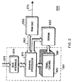
- the generator 200 includes a bus interface 205 for connecting to the bus 125 of Figure 1.
- a specific purpose graphic processor 210 is connected to a random access memory/digital-to-analog converter (RAMDAC) 230.
- the RAMDAC 230 receives digital graphic data on line 260, and produces analog video signals on line 270.
- the graphic processor 210 is also connected to a synchronous dynamic access memory (SDRAM) 220, and texel caches 300.
- SDRAM 220 stores graphic data in maps and buffers.
- the buffers can include front, back, color, Z, stencil, overlay, and format buffers.
- the maps can store texture data (texels).
- the elements 205, 210, and 300 are arranged on a single semiconductor chip 201.
- the generator 200 receives graphic data and instructions from the CPU 110 of Figure 1.
- the data can be stored in the SDRAM 220 as maps and buffers.
- the data of the buffers and maps are combined by the processor 210 to produce graphic data on line 260.
- the texel caches 300 are used to cache texel data.
- each texel cache 300 there is one memory controller 399 for each texel cache 300. If eight texel caches 300 are used, then there will be eight memory controllers 399. In contrast with traditional caches, here the number of lines in each cache is a small integer number, for example, two, three, four, eight, or twelve.
- the caches 300 are configured to separate data and their address tags in space and time using a pipeline. This allows the caches 300 to be non-blocking and have more outstanding "missed" requests than there are lines in the caches 300. This not only improves performance, but also simplifies the design.
- FIG. 3 show one non-blocking pipelined texel cache 300 in a greater level of detail.
- the cache 300 includes an address cache 310.
- the address cache 310 is a fully associative content addressable memory (CAM) which uses twenty-two bits as address tags. In the preferred embodiment, the number of lines in the address cache 310 is small, for example eight.
- the address cache 310 also maintains least recently written information in a wrap-around counter. The least recently written line becomes the next "victim" in case of a miss.
- the cache lines have associated line addresses, for example, 0 to 7.
- the address cache 310 is coupled to an input end (tail) of an address queue 320.
- the address queue 320 is a 22 bit wide first-in-first-out (FIFO) buffer.
- the address queue 320 stores addresses (tags) of the most recently missed accesses.
- the output end (head) of the address queue 320 is coupled to the input of one of the memory controllers 399 of Figure 2.
- the output from the memory controller 399 is connected to an input end (tail) of a data queue 350.
- the data queue is a 32 bit wide FIFO.
- the address cache 310 is also connected to an input end of a probe result queue 330 by lines 302 and 303.
- the probe result queue 330 is an N+1 bits wide FIFO, where N bits on line 303 are used to indicate a particular line of the address cache 310, and one bit on line 302 is used to indicate hit/miss information.
- a data cache 360 and a multiplexer (MUX) 370 both receive input from the head of the probe result queue 330, and the head of the data queue 350.
- the data cache 360 can be implemented as SRAM, an interconnected register file, or a set of latches.
- the MUX 370 is 32 bits wide with multiple inputs and one output on line 309.
- the output of the MUX is selected by the information supplied to the probe result queue 330 via lines 302 and 303 which eventually come out on line 304. In other words, the selection is time-delayed dependent on the signals on lines 302 and 303. The delay being the time for the information to make it to the head of the queue 330. This means that the selection is immediately based on the information in the head entry of the probe result queue.
- the cache 300 receives "probe" addresses associated with read access requests on line 301.
- the probe addresses can be used to probe all lines of the address cache 310 simultaneously. If there is a hit, the hit/miss information on line 302 is set to a logical one (high), otherwise in case of a miss, the line 302 is set to a logical zero.
- the hit line address (N-bits) is expressed on line 303, otherwise, a victim line address is expressed. This means that one N+1 bit entry (line address plus hit/miss information) is placed at the tail of the probe result queue 330 for each cache access, hit or miss.
- the probe address is placed on the address queue 320.
- the address queue 320 drives request made to the high latency SDRAM 220 via the controller 399. Responses from the controller 399 are data at missed addresses. The data are placed in the data queue 350.
- the data cache 360 is accessed using the entries of the probe result queue 330. If the head of the probe result queue indicates a hit, the N bits on line 304 are used as a cache line address to read the requested texel data from the data cache 360. A hit also causes the MUX 370 to select, as its output on line 309, data from the data cache 360 at the selected data cache address.
- the probe entry indicates a miss
- the data of the next FIFO entry of the data queue 350 are stored in the data cache 360 at the cache line address specified in the N bits of the probe queue entry on line 304.
- the MUX 370 selects, as output on line 309, the data from queue 350.
- data are presented on line 309 in the identical order as the data were requested.
- selection can be performed by "transparent" latches that "load” missed data from the data queue 330 into the data cache 360 at the beginning of a cycle, and would allow data from the data queue to "flow" through the latch during the cycle.
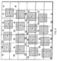
- the "shaded" 2x2 pixel squares T0, ..., T15 in Figure 4 show an example of how sixteen texture-mapped pixels are mapped onto a texture Mipmap, and hence generate texel fetch requests. Each shaded square requires fetching the four texels that the shaded pixel square overlaps.
- the A-J of the labels A0-J3 indicate different 22 bit addresses, and the numbers 0, 1, 2, and 3 represent the different memory controllers 399, and therefore, different caches where the texel data are to be cached.
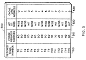
- a table 500 of Figure 5 shows the dynamic hit and miss information 520 for memory controller 0 texel fetch requests.
- column 510 shows the texel fetch request number
- column 515 the probe request addresses
- column 520 the hit or miss indication
- column 530 the cache line address, assuming an eight line cache.
- non-blocking pipelined cache has been described for texel caching. However, the same design can also be used to tile a small source rectangle onto a larger destination rectangle in other graphic applications.
Description
- This invention relates generally to computer system memories, and more particularly to cached memories used in graphic computer systems.
- In a graphic computer system, texture mapping (i.e., "texturing") can increase the realism of three-dimensional (3D) images generated by the system. Example textures can represent wood grains, bricks, carpets, stone walls, grass, and the like. Textures provide a more realistic rendering of the surfaces of image objects. Texturing is performed using an array of texture elements (texels) stored as a texture map in computer memories. The texture map can be synthesized, or obtained from a scanned image.
- A low resolution texture map may include 64x64 texels, while a high resolution map may have 4096x4096 texels. Typically, texels are stored as words of data, the address of each word indicates a particular coordinate of the texture map. The data can represent color (RBG), and, perhaps, transparency information.
- To display a graphic image including objects having textured surfaces, graphic software and hardware converts the surfaces to an array of screen coordinates associated with displayable picture elements (pixels). The pixel coordinates are used to locate corresponding texels of the texel map. The color and transparency values of the corresponding texels are merged with pixel data to determine the color and transparency final values of the displayed pixels. Texel coordinates interior to surfaces can be obtained by interpolating texel coordinates supplied at the vertices of objects.
- In low quality texture mapping called "point-sampling," only one texel is used for each of the pixels of the image. As a result, point-sampled textured images tend to have annoying aliasing artifacts in the way of discernable discontinuities in their textured surfaces. This is particularly true if the surface to be textured is highly distorted, for example, a surface of a 3D image which extends into the distance.
- For high quality texturing, such as tri-linear texture mapping, multiple texel maps may be used, e.g., "Multem In Parvo" (many in place) maps, or Mipmaps. For example, a first high resolution Mipmap of a texture has 1024x1024 texels, the next lesser resolution Mipmap has 512x512 texels, the next 256x256 texels, and so forth, all the way down to a 1x1 low resolution single texel Mipmap for a total of 11 Mipmaps representing a specific texture. From these multiple maps, textures for distorted surfaces can smoothly be interpolated, even if zooming is used to increase or decrease the size of the object to give a sense of three-dimensions.
- High quality texture mapping may require the mapping of eight or sixteen texels to a single pixel. This means that for every pixel the system must access texel data at eight or sixteen memory addresses. Clearly, texturing can consume a large amount of bandwidth of memory systems.
- It would be desirable to reduce the memory bandwidth requirements of texture mapping. This might allow the use of fewer memory chips devoted to textures, the use of less expensive general-purpose low-speed dynamic random access memories (DRAM) to store textures, and to store textures in the same memory as used for other data during image generation.
- Some prior art texture mapping devices store texture maps in dedicated high-speed static random access memories (SRAM). Each read request for texel data makes an access to the SRAM, even if successive data are read from the identical address. SRAMs specifically designed for texture mapping tend to be expensive, highly integrated into the graphic hardware, and of limited functionality.
- In modern DRAM, the sense amplifiers can be used to "cache" data. Caching can take advantage of spatial and temporal localities of data. For example, if a sequence of texel addresses are all in the same DRAM page, then the data can be accessed directly from the sense amplifiers.
- With DRAM, the memory bandwidth for fetches from the same memory page can approach that of SRAM. However, if there is a "miss" on an address of a current page, then another page needs to be accessed. Switching between DRAM pages may require several processor cycles while the data of the next page are fetched and latched into the sense amplifiers. This increases access latencies. Such latencies can be hidden by using long pipelines in the access path if the average bandwidth of the memory system is sufficient to handle page fetches.
- Adding a true cache to the memory system may reduce bandwidth requirements when there are good spatial and temporal localities in the data. However, implementing a cache memory for graphic devices is difficult. If the cache is configured as a traditional blocking cache, then a miss will "stall" further accesses, since the miss must completely be serviced before a next access request can be accepted. This is due to the fact that the fetched data must be latched somewhere before further requests can proceed. If there are a larger number of misses, then stalls will cause the memory system to deliver less bandwidth for texel fetches than a pipelined non-cached memory system.
- If miss-servicing bookkeeping logic is included, then the cache can be made non-blocking. However, a non-blocking cache can be a hindrance if it cannot track as many misses as there are stages in the pipeline, e.g., from the read request to the data becoming available.
- The latency and cache size problems become even worse when the memories not only store texel and pixel data but also other information. If the memories are configured, as desired, from general purpose low-cost DRAM, then many different types of graphic information can be stored there. However, in this case, access requests to the various buffers should be batched to avoided page "thrashing." Batched accesses may delay requests for texel data to further increase latencies and the number of misses that need to be tracked.
- A direct-mapped cache could be used. However, it should be quite large so that addresses are adequately distributed throughout the cache. If the cache is tens of lines, then some data may remain unused for extended periods of time wasting cache, while other data experience frequent conflicts degrading performance. Larger caches also increase cost.
- A non-blocking fully associative content addressable memory (CAM), which uses the full address of the data as a tag, may be more appropriate for texture mapping. But even a fully associative cache needs to be a reasonable size, and latencies on a miss can still cause large delays between the time the read request is issued, and the time the data become available. The peculiarities of texture mapping increases the likelihood of cache misses. In a worse case, each texel is used exactly once, and therefore, each access will cause a miss, so the cache does not provide any benefit at all.
- Therefore, it is desired to provide a cache for graphic systems which can decrease the bandwidth required by texel fetches without the disadvantages of traditional caches.
- US 5526510 describes a data cache having a fill buffer for receiving data retrieved from main memory as a result of a cache miss, and a separate write-back buffer that receives a victim cache line being evicted from the cache, also as a result of a cache miss. The cache is adapted to transfer the victim line into the write-back buffer in the same clock cycle as writing the replacement data from the fill buffer to avoid problems with latency between cache line transfers.
- IBM Technical Disclosure Bulletin, Vol 39,
No 3, March 1996, pp 19, 20 describes a compression cache miss bypass that allows commands that access a cache hit line to bypass and be executed ahead of previously received commands that attempt to access a cache miss line. Miss commands are moved to a separate queue. - The present invention, in its broad form, resides in an apparatus for caching data, as recited in
claim 1, and in a method for caching data, as recited in claim 9. - Described hereinafter is a non-blocking pipelined cache which can be used in a graphic processor for accessing texel data. The non-blocking pipelined cache preferably maintains texel addresses and data in address and data caches connected to each other by first-in-first-out queues. The addresses and data are advantageously maintained in a spatial and temporal separate manner, as described hereinafter.
- The address cache includes a plurality of lines. Each line can store a memory address specified in read requests. Associated with each line is a line address. A first queue has an input connected to the address cache and an output connected to a memory controller. The first queue stores missed memory addresses due to read request misses. The missed memory addresses are forwarded to the memory controller. A second queue connected to the memory controller receives data stored at the missed memory addresses.
- A third queue connected to the address cache, for each read request, stores a line address and hit/miss information. The hit/miss information indicates whether or not a particular requested address is stored in the address queue.
- A data cache is connected to the output of the second and third queues. The data cache stores the data at the missed memory addresses received from the second queue. A multiplexer selects data to output from the data cache or the second queue depending on the hit/miss information stored in the third queue.
- A more detailed understanding of the invention may be had from the following description of a preferred embodiment, given by way of example, and to be understood with reference to the accompanying drawing wherein:
- Figure 1 is a block diagram of a graphic display system which uses a non-blocking pipelined cache according to a preferred embodiment of the invention;
- Figure 2 is a block diagram of a graphic generator of the system of Figure 1;
- Figure 3 is a block diagram of a non-blocking pipeline cache according to a preferred embodiment of the invention;
- Figure 4 is a diagram of texel fetches from a texture map; and
- Figure 5 is a table of hit/miss information associated with an eight-line cache.
- Now with reference to Figure 1, a preferred embodiment of a non-blocking pipelined cached according to the invention is described in detail. A
graphic display system 100 includes a general purpose central processing unit (CPU) 110 connected to amain memory 120 by amemory bus 115. TheCPU 110 is also connected togeneral purpose bus 125, for example, a PCI bus. Thebus 125 can be connected to adisk subsystem 130, an input/output (I/O)subsystem 140, and agraphic generator 200. Thegraphic generator 200 is connected to agraphic display device 150 byline 270. Thesystem 100 can be configured as a graphic workstation. - The
CPU 110 can include one or more general purpose processor chips, for example, ALPHA processors from Digital Equipment Corporation, Maynard, MA. Themain memory 120 is for storing machine executable instructions and data while thesystem 100 is operating. Thedisk 130 persistently stores the instructions and data in files. The instructions and data can be obtained via the I/O subsystem 140. The I/O system can also connect to I/O devices (not shown) such as a keyboard, mouse, or joy-stick to control the operation of thesystem 100. Thebuses - During operation of the
system 100, the instructions of software programs are executed by theCPU 110. The programs are designed to generate graphic images on thedisplay device 150. The data for the images, and instructions on how to render the images are transferred to thegraphic generator 200 via thebuses generator 200 converts the digital data to analog signals which can drive thedisplay device 150. More specifically, thegraphic generator 200 renders three-dimensional images at high-speed. - As shown in Figure 2, the
generator 200 includes abus interface 205 for connecting to thebus 125 of Figure 1. A specific purposegraphic processor 210 is connected to a random access memory/digital-to-analog converter (RAMDAC) 230. TheRAMDAC 230 receives digital graphic data online 260, and produces analog video signals online 270. - The
graphic processor 210 is also connected to a synchronous dynamic access memory (SDRAM) 220, andtexel caches 300. TheSDRAM 220 stores graphic data in maps and buffers. The buffers can include front, back, color, Z, stencil, overlay, and format buffers. The maps can store texture data (texels). Preferably, theelements single semiconductor chip 201. - During operation, the
generator 200 receives graphic data and instructions from theCPU 110 of Figure 1. The data can be stored in theSDRAM 220 as maps and buffers. The data of the buffers and maps are combined by theprocessor 210 to produce graphic data online 260. Because of the large numbers of texels accessed, and in order to improve system performance, thetexel caches 300 are used to cache texel data. - In one embodiment, there is one
memory controller 399 for eachtexel cache 300. If eighttexel caches 300 are used, then there will be eightmemory controllers 399. In contrast with traditional caches, here the number of lines in each cache is a small integer number, for example, two, three, four, eight, or twelve. - In order to deal with small
sized caches 300 and long memory latencies, thecaches 300 are configured to separate data and their address tags in space and time using a pipeline. This allows thecaches 300 to be non-blocking and have more outstanding "missed" requests than there are lines in thecaches 300. This not only improves performance, but also simplifies the design. - Figure 3 show one non-blocking pipelined
texel cache 300 in a greater level of detail. Thecache 300 includes anaddress cache 310. Theaddress cache 310 is a fully associative content addressable memory (CAM) which uses twenty-two bits as address tags. In the preferred embodiment, the number of lines in theaddress cache 310 is small, for example eight. Theaddress cache 310 also maintains least recently written information in a wrap-around counter. The least recently written line becomes the next "victim" in case of a miss. The cache lines have associated line addresses, for example, 0 to 7. - The
address cache 310 is coupled to an input end (tail) of anaddress queue 320. Theaddress queue 320 is a 22 bit wide first-in-first-out (FIFO) buffer. Theaddress queue 320 stores addresses (tags) of the most recently missed accesses. - The output end (head) of the
address queue 320 is coupled to the input of one of thememory controllers 399 of Figure 2. The output from thememory controller 399 is connected to an input end (tail) of adata queue 350. The data queue is a 32 bit wide FIFO. - The
address cache 310 is also connected to an input end of aprobe result queue 330 bylines probe result queue 330 is an N+1 bits wide FIFO, where N bits online 303 are used to indicate a particular line of theaddress cache 310, and one bit online 302 is used to indicate hit/miss information. - A
data cache 360 and a multiplexer (MUX) 370 both receive input from the head of theprobe result queue 330, and the head of thedata queue 350. Thedata cache 360 can be implemented as SRAM, an interconnected register file, or a set of latches. TheMUX 370 is 32 bits wide with multiple inputs and one output online 309. The output of the MUX is selected by the information supplied to theprobe result queue 330 vialines line 304. In other words, the selection is time-delayed dependent on the signals onlines queue 330. This means that the selection is immediately based on the information in the head entry of the probe result queue. - During operation, the
cache 300 receives "probe" addresses associated with read access requests online 301. The probe addresses can be used to probe all lines of theaddress cache 310 simultaneously. If there is a hit, the hit/miss information online 302 is set to a logical one (high), otherwise in case of a miss, theline 302 is set to a logical zero. - In case of a hit, the hit line address (N-bits) is expressed on
line 303, otherwise, a victim line address is expressed. This means that oneN+ 1 bit entry (line address plus hit/miss information) is placed at the tail of theprobe result queue 330 for each cache access, hit or miss. In case of a miss, the probe address is placed on theaddress queue 320. Theaddress queue 320 drives request made to thehigh latency SDRAM 220 via thecontroller 399. Responses from thecontroller 399 are data at missed addresses. The data are placed in thedata queue 350. - The
data cache 360 is accessed using the entries of theprobe result queue 330. If the head of the probe result queue indicates a hit, the N bits online 304 are used as a cache line address to read the requested texel data from thedata cache 360. A hit also causes theMUX 370 to select, as its output online 309, data from thedata cache 360 at the selected data cache address. - If the probe entry indicates a miss, then the data of the next FIFO entry of the
data queue 350 are stored in thedata cache 360 at the cache line address specified in the N bits of the probe queue entry online 304. In this case, theMUX 370 selects, as output online 309, the data fromqueue 350. In either the hit or miss case, data are presented online 309 in the identical order as the data were requested. - Other means for selecting can also be used. For example, the selection can be performed by "transparent" latches that "load" missed data from the
data queue 330 into thedata cache 360 at the beginning of a cycle, and would allow data from the data queue to "flow" through the latch during the cycle. - If there is a hit on the
address cache 310, or theaddress queue 320 is not full, then new read requests can be accepted. If there is a miss in theaddress cache 310 and theaddress queue 320 is full, then the read request must be stalled until space becomes available in theaddress queue 320. If there is a hit in thedata cache 360, or thedata queue 350 is not empty, then the reply data are available. If there is a miss in thedata cache 360, and thedata queue 350 is empty, then the reply must be stalled until data become available in thedata queue 350. - The "shaded" 2x2 pixel squares T0, ..., T15 in Figure 4 show an example of how sixteen texture-mapped pixels are mapped onto a texture Mipmap, and hence generate texel fetch requests. Each shaded square requires fetching the four texels that the shaded pixel square overlaps.
- The A-J of the labels A0-J3 indicate different 22 bit addresses, and the
numbers different memory controllers 399, and therefore, different caches where the texel data are to be cached. - If there are eight lines in each
cache 300, then the hit to miss ratio will be good. Even a two line cache will give good performance when the texels are fetched in an appropriate manner. - A table 500 of Figure 5 shows the dynamic hit and miss information 520 for memory controller 0 texel fetch requests. In Figure 5,
column 510 shows the texel fetch request number,column 515 the probe request addresses, column 520 the hit or miss indication, and column 530 the cache line address, assuming an eight line cache. - The utility of the non-blocking pipelined cache has been described for texel caching. However, the same design can also be used to tile a small source rectangle onto a larger destination rectangle in other graphic applications.
Claims (9)
- An apparatus (300) for caching and retrieving data, comprising:wherein said data selected by said means (370) for selecting output are, in the case of either a hit or a miss, in the identical order as the data were requested at said address cache (310).an address cache (310) for receiving read requests, including a plurality of lines for storing memory addresses specified in said read requests, the lines having associated line addresses;an address queue (320), connected to the address cache and to a memory controller (399), for storing each of the memory addresses received from the address cache that correspond to read request misses in the address cache (310), and for forwarding each of the missed memory addresses to the memory controller;the memory controller (399) adapted to effect retrieval of data corresponding to each of the missed memory addresses from a memory (220);a data queue (350), connected to the memory controller (399), for storing the data corresponding to each of the missed memory addresses, received from the memory controller;a probe result queue (330), connected to said address cache (310), for storing the line address information and hit/miss information received from the address cache (310) corresponding to each of the read requests received at the address cache (310);a data cache (360), connected to the data queue and the probe result queue, for storing the data corresponding to each of said missed memory addresses received from said data queue; andmeans (370), connected to the data queue, the probe result queue and the data cache for selecting output from the data cache (360) when the information stored in the head entry of the probe result queue indicates a hit, or from the data queue (350) when the information stored in the head entry of the probe result queue indicates a miss, said data when being selected from said data queue (350) being also stored in the data cache (360) at the cache line address of said head entry, to provide a non-blocking pipelined cache,
- The apparatus as in claim 1 wherein the address cache (310) is a fully associative content addressable memory, wherein the memory addresses are stored as tags.
- The apparatus as in claim 1 wherein the probe result queue (330) further comprises:a plurality of entries, each entry being N+1 bits wide, where N bits indicate a particular line address and one bit indicates the hit/miss information.
- The apparatus as in claim 1 wherein the data cache (360) is an interconnected register file.
- The apparatus as in claim 1 wherein the data stored are texel data.
- The apparatus as in claim 1 further comprising a synchronous dynamic access memory (220) for storing the data.
- The apparatus of claim 1 wherein the data at the missed addresses is responded to in the order of the misses.
- The apparatus of claim 1 wherein the plurality of lines is maintained in a least recently written order.
- A method for caching and retrieving data comprising the steps of:wherein said selected data are, in either the case of a hit or a miss, in the identical order as the data were requested at said address cache (310).storing, in an address cache (310), memory addresses specified in read requests received at said address cache (310), said address cache comprising a plurality of lines, the lines having associated line addresses;queuing, in an address queue (320), each of the memory addresses received from the address cache that correspond to read request misses in the address cache;forwarding each of the missed memory addresses to a memory controller (399) and retrieving data corresponding to each of the missed memory addresses from a memory (220) by the memory controller;queuing the data corresponding to each of the missed memory addresses retrieved by the memory controller (399) in a data queue (350);queueing the line address information and hit/miss information corresponding to each of the read requests received from the address cache (310), in a probe result queue (330);storing, in a data cache (360), the data corresponding to each of the missed memory addresses received from the data queue; andselecting, by means (370) connected to the data queue, the probe result queue and the data cache, output from the data cache (360) when the information stored in the head entry of the probe result queue indicates a hit, or from said data queue (350) when the information stored in the head entry of the probe result queue indicates a miss,said data, when being selected from said data queue (350), also being stored in the data cache (360) at the cache line address of said head entry, to provide a non-blocking pipelined cache, and
Applications Claiming Priority (2)
| Application Number | Priority Date | Filing Date | Title |
|---|---|---|---|
| US08/870,152 US6085292A (en) | 1997-06-05 | 1997-06-05 | Apparatus and method for providing non-blocking pipelined cache |
| US870152 | 1997-06-05 |
Publications (3)
| Publication Number | Publication Date |
|---|---|
| EP0883065A2 EP0883065A2 (en) | 1998-12-09 |
| EP0883065A3 EP0883065A3 (en) | 1999-01-20 |
| EP0883065B1 true EP0883065B1 (en) | 2003-03-19 |
Family
ID=25354879
Family Applications (1)
| Application Number | Title | Priority Date | Filing Date |
|---|---|---|---|
| EP98303741A Expired - Lifetime EP0883065B1 (en) | 1997-06-05 | 1998-05-13 | Non-blocking pipelined cache |
Country Status (5)
| Country | Link |
|---|---|
| US (1) | US6085292A (en) |
| EP (1) | EP0883065B1 (en) |
| JP (1) | JP4545242B2 (en) |
| CA (1) | CA2238586A1 (en) |
| DE (1) | DE69812223T2 (en) |
Families Citing this family (22)
| Publication number | Priority date | Publication date | Assignee | Title |
|---|---|---|---|---|
| US7136068B1 (en) | 1998-04-07 | 2006-11-14 | Nvidia Corporation | Texture cache for a computer graphics accelerator |
| US6490652B1 (en) * | 1999-02-03 | 2002-12-03 | Ati Technologies Inc. | Method and apparatus for decoupled retrieval of cache miss data |
| US6919895B1 (en) | 1999-03-22 | 2005-07-19 | Nvidia Corporation | Texture caching arrangement for a computer graphics accelerator |
| US6266744B1 (en) | 1999-05-18 | 2001-07-24 | Advanced Micro Devices, Inc. | Store to load forwarding using a dependency link file |
| US6473832B1 (en) * | 1999-05-18 | 2002-10-29 | Advanced Micro Devices, Inc. | Load/store unit having pre-cache and post-cache queues for low latency load memory operations |
| US6473837B1 (en) | 1999-05-18 | 2002-10-29 | Advanced Micro Devices, Inc. | Snoop resynchronization mechanism to preserve read ordering |
| US6442673B1 (en) * | 1999-11-05 | 2002-08-27 | I.P. First L.L.C. | Update forwarding cache for address mode |
| US6593931B1 (en) * | 1999-12-01 | 2003-07-15 | Intel Corporation | Method and apparatus for improving system memory bandwidth utilization during graphics translational lookaside buffer cache miss fetch cycles |
| US6757793B1 (en) * | 2000-03-29 | 2004-06-29 | Advanced Micro Devices, Inc. | Reducing probe traffic in multiprocessor systems using a victim record table |
| US6549985B1 (en) * | 2000-03-30 | 2003-04-15 | I P - First, Llc | Method and apparatus for resolving additional load misses and page table walks under orthogonal stalls in a single pipeline processor |
| US6629234B1 (en) | 2000-03-30 | 2003-09-30 | Ip. First, L.L.C. | Speculative generation at address generation stage of previous instruction result stored in forward cache for use by succeeding address dependent instruction |
| US7107438B2 (en) * | 2003-02-04 | 2006-09-12 | Via Technologies, Inc. | Pipelined microprocessor, apparatus, and method for performing early correction of conditional branch instruction mispredictions |
| US7185182B2 (en) * | 2003-02-04 | 2007-02-27 | Via Technologies, Inc. | Pipelined microprocessor, apparatus, and method for generating early instruction results |
| US7100024B2 (en) | 2003-02-04 | 2006-08-29 | Via Technologies, Inc. | Pipelined microprocessor, apparatus, and method for generating early status flags |
| US6933945B2 (en) * | 2003-03-31 | 2005-08-23 | Sun Microsystems, Inc. | Design for a non-blocking cache for texture mapping |
| US20050216713A1 (en) * | 2004-03-25 | 2005-09-29 | International Business Machines Corporation | Instruction text controlled selectively stated branches for prediction via a branch target buffer |
| US20050270870A1 (en) * | 2004-06-02 | 2005-12-08 | Sangho Shin | Time slot interchange switch with cache |
| US7944876B2 (en) * | 2004-06-02 | 2011-05-17 | Integrated Device Technology, Inc | Time slot interchange switch with bit error rate testing |
| US20080218527A1 (en) * | 2007-03-09 | 2008-09-11 | Romanick Ian D | Method and Apparatus for Improving Hit Rates of a Cache Memory for Storing Texture Data During Graphics Rendering |
| US8966230B2 (en) * | 2009-09-30 | 2015-02-24 | Intel Corporation | Dynamic selection of execution stage |
| KR102061069B1 (en) | 2013-02-28 | 2020-01-02 | 삼성전자주식회사 | Texture cache memory system of non-blocking for texture mapping pipeline and operation method of the texture cache memory |
| US11494224B2 (en) * | 2019-05-24 | 2022-11-08 | Texas Instruments Incorporated | Controller with caching and non-caching modes |
Family Cites Families (19)
| Publication number | Priority date | Publication date | Assignee | Title |
|---|---|---|---|---|
| US5148536A (en) * | 1988-07-25 | 1992-09-15 | Digital Equipment Corporation | Pipeline having an integral cache which processes cache misses and loads data in parallel |
| JPH03217985A (en) * | 1990-01-23 | 1991-09-25 | Hitachi Ltd | Data processor and image diagnostic device |
| EP0449540B1 (en) * | 1990-03-27 | 2000-05-17 | Digital Equipment Corporation | Memory system and method with prefetch buffer |
| DE4306077A1 (en) * | 1992-02-27 | 1993-09-02 | Hewlett Packard Co | |
| US5353426A (en) * | 1992-04-29 | 1994-10-04 | Sun Microsystems, Inc. | Cache miss buffer adapted to satisfy read requests to portions of a cache fill in progress without waiting for the cache fill to complete |
| US5544342A (en) * | 1993-06-30 | 1996-08-06 | International Business Machines Corporation | System and method for prefetching information in a processing system |
| US5555392A (en) * | 1993-10-01 | 1996-09-10 | Intel Corporation | Method and apparatus for a line based non-blocking data cache |
| US5555391A (en) * | 1993-12-23 | 1996-09-10 | Unisys Corporation | System and method for storing partial blocks of file data in a file cache system by merging partial updated blocks with file block to be written |
| JP3733604B2 (en) * | 1993-12-27 | 2006-01-11 | 松下電器産業株式会社 | Cache memory |
| US5826109A (en) * | 1994-01-04 | 1998-10-20 | Intel Corporation | Method and apparatus for performing multiple load operations to the same memory location in a computer system |
| US5526510A (en) * | 1994-02-28 | 1996-06-11 | Intel Corporation | Method and apparatus for implementing a single clock cycle line replacement in a data cache unit |
| US5671444A (en) * | 1994-02-28 | 1997-09-23 | Intel Corporaiton | Methods and apparatus for caching data in a non-blocking manner using a plurality of fill buffers |
| US5559987A (en) * | 1994-06-30 | 1996-09-24 | Digital Equipment Corporation | Method and apparatus for updating a duplicate tag status in a snoop bus protocol based computer system |
| EP0741356A1 (en) * | 1995-05-05 | 1996-11-06 | Rockwell International Corporation | Cache architecture and method of operation |
| EP0747825B1 (en) * | 1995-06-06 | 2001-09-19 | Hewlett-Packard Company, A Delaware Corporation | SDRAM data allocation system and method |
| US5790130A (en) * | 1995-06-08 | 1998-08-04 | Hewlett-Packard Company | Texel cache interrupt daemon for virtual memory management of texture maps |
| JPH08339331A (en) * | 1995-06-12 | 1996-12-24 | Alps Lsi Technol Kk | Cache memory |
| US5752069A (en) * | 1995-08-31 | 1998-05-12 | Advanced Micro Devices, Inc. | Superscalar microprocessor employing away prediction structure |
| US5829029A (en) * | 1996-12-18 | 1998-10-27 | Bull Hn Information Systems Inc. | Private cache miss and access management in a multiprocessor system with shared memory |
-
1997
- 1997-06-05 US US08/870,152 patent/US6085292A/en not_active Expired - Lifetime
-
1998
- 1998-05-13 DE DE69812223T patent/DE69812223T2/en not_active Expired - Lifetime
- 1998-05-13 EP EP98303741A patent/EP0883065B1/en not_active Expired - Lifetime
- 1998-05-25 CA CA002238586A patent/CA2238586A1/en not_active Abandoned
- 1998-06-03 JP JP15440898A patent/JP4545242B2/en not_active Expired - Fee Related
Also Published As
| Publication number | Publication date |
|---|---|
| DE69812223T2 (en) | 2004-01-22 |
| DE69812223D1 (en) | 2003-04-24 |
| EP0883065A3 (en) | 1999-01-20 |
| JPH11102435A (en) | 1999-04-13 |
| CA2238586A1 (en) | 1998-12-05 |
| EP0883065A2 (en) | 1998-12-09 |
| US6085292A (en) | 2000-07-04 |
| JP4545242B2 (en) | 2010-09-15 |
Similar Documents
| Publication | Publication Date | Title |
|---|---|---|
| EP0883065B1 (en) | Non-blocking pipelined cache | |
| US6104418A (en) | Method and system for improved memory interface during image rendering | |
| US6426753B1 (en) | Cache memory for high latency and out-of-order return of texture data | |
| US6288730B1 (en) | Method and apparatus for generating texture | |
| US7050063B1 (en) | 3-D rendering texture caching scheme | |
| US6011565A (en) | Non-stalled requesting texture cache | |
| US6204863B1 (en) | Method for dynamic XY tiled texture caching | |
| US5831640A (en) | Enhanced texture map data fetching circuit and method | |
| US6856320B1 (en) | Demand-based memory system for graphics applications | |
| US5579473A (en) | Interface controller for frame buffer random access memory devices | |
| US7415575B1 (en) | Shared cache with client-specific replacement policy | |
| US6674443B1 (en) | Memory system for accelerating graphics operations within an electronic device | |
| US6650333B1 (en) | Multi-pool texture memory management | |
| US20030169263A1 (en) | System and method for prefetching data from a frame buffer | |
| US6795078B2 (en) | Parallel read with source-clear operation | |
| US6741256B2 (en) | Predictive optimizer for DRAM memory | |
| EP1721298A2 (en) | Embedded system with 3d graphics core and local pixel buffer | |
| US6720969B2 (en) | Dirty tag bits for 3D-RAM SRAM | |
| US6300953B1 (en) | Apparatus and method for grouping texture cache requests | |
| US6167498A (en) | Circuits systems and methods for managing data requests between memory subsystems operating in response to multiple address formats | |
| US6683615B1 (en) | Doubly-virtualized texture memory | |
| US6778179B2 (en) | External dirty tag bits for 3D-RAM SRAM | |
| US20040239680A1 (en) | Method for improving cache-miss performance | |
| US7710425B1 (en) | Graphic memory management with invisible hardware-managed page faulting | |
| WO1998028713A1 (en) | Enhanced methods and systems for caching and pipelining of graphics texture data |
Legal Events
| Date | Code | Title | Description |
|---|---|---|---|
| PUAI | Public reference made under article 153(3) epc to a published international application that has entered the european phase |
Free format text: ORIGINAL CODE: 0009012 |
|
| PUAL | Search report despatched |
Free format text: ORIGINAL CODE: 0009013 |
|
| AK | Designated contracting states |
Kind code of ref document: A2 Designated state(s): DE FR GB |
|
| AX | Request for extension of the european patent |
Free format text: AL;LT;LV;MK;RO;SI |
|
| AK | Designated contracting states |
Kind code of ref document: A3 Designated state(s): AT BE CH CY DE DK ES FI FR GB GR IE IT LI LU MC NL PT SE |
|
| AX | Request for extension of the european patent |
Free format text: AL;LT;LV;MK;RO;SI |
|
| 17P | Request for examination filed |
Effective date: 19990719 |
|
| AKX | Designation fees paid |
Free format text: DE FR GB |
|
| RAP1 | Party data changed (applicant data changed or rights of an application transferred) |
Owner name: COMPAQ COMPUTER CORPORATION |
|
| 17Q | First examination report despatched |
Effective date: 20010730 |
|
| GRAG | Despatch of communication of intention to grant |
Free format text: ORIGINAL CODE: EPIDOS AGRA |
|
| GRAG | Despatch of communication of intention to grant |
Free format text: ORIGINAL CODE: EPIDOS AGRA |
|
| GRAG | Despatch of communication of intention to grant |
Free format text: ORIGINAL CODE: EPIDOS AGRA |
|
| GRAH | Despatch of communication of intention to grant a patent |
Free format text: ORIGINAL CODE: EPIDOS IGRA |
|
| GRAH | Despatch of communication of intention to grant a patent |
Free format text: ORIGINAL CODE: EPIDOS IGRA |
|
| GRAA | (expected) grant |
Free format text: ORIGINAL CODE: 0009210 |
|
| AK | Designated contracting states |
Designated state(s): DE FR GB |
|
| REG | Reference to a national code |
Ref country code: GB Ref legal event code: FG4D |
|
| REF | Corresponds to: |
Ref document number: 69812223 Country of ref document: DE Date of ref document: 20030424 Kind code of ref document: P |
|
| ET | Fr: translation filed | ||
| PLBE | No opposition filed within time limit |
Free format text: ORIGINAL CODE: 0009261 |
|
| STAA | Information on the status of an ep patent application or granted ep patent |
Free format text: STATUS: NO OPPOSITION FILED WITHIN TIME LIMIT |
|
| 26N | No opposition filed |
Effective date: 20031222 |
|
| REG | Reference to a national code |
Ref country code: GB Ref legal event code: 732E |
|
| PGFP | Annual fee paid to national office [announced via postgrant information from national office to epo] |
Ref country code: FR Payment date: 20110607 Year of fee payment: 14 |
|
| PGFP | Annual fee paid to national office [announced via postgrant information from national office to epo] |
Ref country code: GB Payment date: 20110525 Year of fee payment: 14 |
|
| PGFP | Annual fee paid to national office [announced via postgrant information from national office to epo] |
Ref country code: DE Payment date: 20110527 Year of fee payment: 14 |
|
| REG | Reference to a national code |
Ref country code: DE Ref legal event code: R082 Ref document number: 69812223 Country of ref document: DE Representative=s name: BOEHMERT & BOEHMERT ANWALTSPARTNERSCHAFT MBB -, DE Effective date: 20120329 Ref country code: DE Ref legal event code: R082 Ref document number: 69812223 Country of ref document: DE Representative=s name: BOEHMERT & BOEHMERT, DE Effective date: 20120329 Ref country code: DE Ref legal event code: R081 Ref document number: 69812223 Country of ref document: DE Owner name: HEWLETT-PACKARD DEVELOPMENT COMPANY, L.P., HOU, US Free format text: FORMER OWNER: COMPAQ COMPUTER CORP., HOUSTON, TEX., US Effective date: 20120329 Ref country code: DE Ref legal event code: R081 Ref document number: 69812223 Country of ref document: DE Owner name: HEWLETT-PACKARD DEVELOPMENT CO., L.P., US Free format text: FORMER OWNER: COMPAQ COMPUTER CORP., HOUSTON, US Effective date: 20120329 |
|
| GBPC | Gb: european patent ceased through non-payment of renewal fee |
Effective date: 20120513 |
|
| REG | Reference to a national code |
Ref country code: FR Ref legal event code: ST Effective date: 20130131 |
|
| REG | Reference to a national code |
Ref country code: DE Ref legal event code: R119 Ref document number: 69812223 Country of ref document: DE Effective date: 20121201 |
|
| PG25 | Lapsed in a contracting state [announced via postgrant information from national office to epo] |
Ref country code: GB Free format text: LAPSE BECAUSE OF NON-PAYMENT OF DUE FEES Effective date: 20120513 Ref country code: FR Free format text: LAPSE BECAUSE OF NON-PAYMENT OF DUE FEES Effective date: 20120531 |
|
| PG25 | Lapsed in a contracting state [announced via postgrant information from national office to epo] |
Ref country code: DE Free format text: LAPSE BECAUSE OF NON-PAYMENT OF DUE FEES Effective date: 20121201 |