EP0881726B1 - Direct amplitude modulation of lasers - Google Patents
Direct amplitude modulation of lasers Download PDFInfo
- Publication number
- EP0881726B1 EP0881726B1 EP98303274A EP98303274A EP0881726B1 EP 0881726 B1 EP0881726 B1 EP 0881726B1 EP 98303274 A EP98303274 A EP 98303274A EP 98303274 A EP98303274 A EP 98303274A EP 0881726 B1 EP0881726 B1 EP 0881726B1
- Authority
- EP
- European Patent Office
- Prior art keywords
- laser
- data
- plane
- respect
- data component
- Prior art date
- Legal status (The legal status is an assumption and is not a legal conclusion. Google has not performed a legal analysis and makes no representation as to the accuracy of the status listed.)
- Expired - Lifetime
Links
Images




Classifications
-
- H—ELECTRICITY
- H01—ELECTRIC ELEMENTS
- H01S—DEVICES USING THE PROCESS OF LIGHT AMPLIFICATION BY STIMULATED EMISSION OF RADIATION [LASER] TO AMPLIFY OR GENERATE LIGHT; DEVICES USING STIMULATED EMISSION OF ELECTROMAGNETIC RADIATION IN WAVE RANGES OTHER THAN OPTICAL
- H01S5/00—Semiconductor lasers
- H01S5/06—Arrangements for controlling the laser output parameters, e.g. by operating on the active medium
- H01S5/062—Arrangements for controlling the laser output parameters, e.g. by operating on the active medium by varying the potential of the electrodes
- H01S5/0625—Arrangements for controlling the laser output parameters, e.g. by operating on the active medium by varying the potential of the electrodes in multi-section lasers
-
- H—ELECTRICITY
- H01—ELECTRIC ELEMENTS
- H01S—DEVICES USING THE PROCESS OF LIGHT AMPLIFICATION BY STIMULATED EMISSION OF RADIATION [LASER] TO AMPLIFY OR GENERATE LIGHT; DEVICES USING STIMULATED EMISSION OF ELECTROMAGNETIC RADIATION IN WAVE RANGES OTHER THAN OPTICAL
- H01S5/00—Semiconductor lasers
- H01S5/06—Arrangements for controlling the laser output parameters, e.g. by operating on the active medium
- H01S5/062—Arrangements for controlling the laser output parameters, e.g. by operating on the active medium by varying the potential of the electrodes
- H01S5/0625—Arrangements for controlling the laser output parameters, e.g. by operating on the active medium by varying the potential of the electrodes in multi-section lasers
- H01S5/06251—Amplitude modulation
-
- H—ELECTRICITY
- H01—ELECTRIC ELEMENTS
- H01S—DEVICES USING THE PROCESS OF LIGHT AMPLIFICATION BY STIMULATED EMISSION OF RADIATION [LASER] TO AMPLIFY OR GENERATE LIGHT; DEVICES USING STIMULATED EMISSION OF ELECTROMAGNETIC RADIATION IN WAVE RANGES OTHER THAN OPTICAL
- H01S5/00—Semiconductor lasers
- H01S5/06—Arrangements for controlling the laser output parameters, e.g. by operating on the active medium
- H01S5/062—Arrangements for controlling the laser output parameters, e.g. by operating on the active medium by varying the potential of the electrodes
- H01S5/0625—Arrangements for controlling the laser output parameters, e.g. by operating on the active medium by varying the potential of the electrodes in multi-section lasers
- H01S5/06255—Controlling the frequency of the radiation
- H01S5/06258—Controlling the frequency of the radiation with DFB-structure
Definitions
- This invention relates to the control of chirp in high speed amplitude modulation of DFB lasers.
- Modulation of the injection current of a semiconductor distributed feedback (DFB) laser is liable to produce variation in both the intensity and the wavelength of its emission. This wavelength variation is called chirp. Chirp imposes bandwidth limitations in amplitude modulated transmission systems that exhibit wavelength dispersion.
- DFB distributed feedback
- the paper states that differences in modulation efficiencies make it possible to modulate amplitude and frequency independently by adjusting the modulation current amplitude and phase applied to the divided electrode structure, and illustrates achieving amplitude modulation with minimum chirp by applying a first signal to the front portion of the divided electrode slightly ahead in phase of the application of a second signal of smaller amplitude to the centre portion of the divided electrode structure.
- frequency modulation with minimum amplitude modulation is described as being achieved with the first current being of larger amplitude than the second and in substantial antiphase (push-pull) relationship.
- a paper that does address this dynamic chirp problem is the paper by I H White et al entitled 'Line Narrowed Picosecond Optical Pulse Generation Using Three Contact InGaAsP/InP multi-quantum Well distributed Feedback Laser under Gain Switching', Electronics Letters Vol. 28, No 13, pages 1257-8.
- the laser has a three section top electrode, of which the two end sections are electrically commoned.
- Dynamic chirp is reduced by arranging to gain-switch the commoned end sections while a constant bias is applied to the middle section in such a way as to provide an effective optical injection locking mechanism.
- the central region causes locking of the wavelength of gain-switched pulses generated by the electrical modulation applied to the end regions. This reduces chirp, but insofar as it still leaves a modulation of the photon population, the approach is not fully effective.
- United States Patent No. 5 502 741 is directed to the control of chirp and describes a method of amplitude modulating the optical emission of a DFB laser in such a way as to minimise dynamic chirp.
- a DFB laser is provided with a top electrode divided symmetrically into two or three in-line separate elements through which a bias current is applied with a symmetrical distribution and through which a modulation current is applied with an antisymmetric (push-pull) distribution.
- the present invention particularly relates to the provision of a method of amplitude modulating the optical emission of a DFB laser in such a way as to optimise dynamic chirp.
- the DFB laser will be at the transmitter end of an optical transmission system, and optimised chirp will be the chirp that provides minimised eye closure penalty at the receiver end.
- optimised chirp condition will not be the same as the condition providing minimised dynamic chirp in the output from the DFB laser.
- a method of amplitude modulating a distributed feedback (DFB) injection laser whose optical cavity has a plane of substantial symmetry normal to the optical emission axis of the laser, in which method a bias current, which is distributed substantially symmetrically with respect to said plane of substantial symmetry is applied to the DFB optical cavity, upon which bias current is superimposed a modulation current that consists of data and inverse data components, wherein the data component has a distribution that is asymmetrically weighted with respect to the plane of substantial symmetry and the inverse data component has a distribution that is a replica of the data component, wherein the data and inverse data components are applied with mirror symmetry with respect to the plane of substantial symmetry, characterised in that the data component is applied in phase-shifted relationship with respect to the application of the inverse data component so that the components operate in phase-shifted push-pull mode in order to optimise the dynamic chirp.
- DFB distributed feedback
- the data and inverse data components of the modulation current are not necessarily of equal amplitude.
- the invention as defined in claim 3 also provides a distributed feedback (DFB) injection laser provided with an electrode structure by means of which current can be injected into the DFB laser's optical cavity to cause the laser to lase, wherein said structure is a divided structure that permits the current injection to be established with a distribution along the optical emission axis of the laser's optical cavity that can be varied, wherein the optical cavity has a plane of substantial symmetry normal to the optical emission axis, which DFB laser is provided with drive means adapted to apply to the divided electrode structure a bias current disposed symmetrically with respect to the plane of substantial symmetry, to superimpose upon said bias current a modulation current that consists of data and inverse data components, wherein the data component has a distribution that is asymmetrically weighted with respect to the plane of substantial symmetry and the inverse data component has a distribution that is a replica of the data component, and to apply the data and inverse data components with mirror symmetry with respect to the plane of substantial symmetry, which drive means is characterised in that it is
- the invention as defined in claim 5 further resides in an optical transmission system incorporating a laser as set out in the preceding paragraph.
- the basic elements of an optical transmission system are depicted in Figure 1, and comprise a transmitter 10 optically coupled with an optical receiver 11 by means of a transmission path 12.
- a transmission path may include a concatenation of optical amplifiers 13.
- the transmitter 10 includes at least one directly modulated DFB semiconductor laser (not separately illustrated in Figure 1) and, in the case of a transmitter for a wavelength division multiplexed transmission system, will contain more than one of such lasers.
- a preferred form of basic semiconductor structure of DFB laser to which the method of amplitude modulation according to the present invention is applied is a conventional DFB laser structure with the single major difference that preferably the distributed feedback grating is without any phase shift.
- Such a basic semiconductor structure may for instance comprise, as depicted in Figure 2, an n-type InP substrate 20 upon which is grown a series of epitaxially deposited layers commencing with an n-type InP buffer layer 21. On top of the buffer layer is grown an undoped quaternary lower waveguide layer 22, a multi-quantum well (MQW) structure 23, an undoped quaternary upper waveguide layer 24, a p-type InP cladding layer 25 and a p-type ternary contact layer 26.
- MQW multi-quantum well
- the MQW structure 23 may typically comprise about six quantum strained or unstrained well layers of ternary or quaternary material sandwiched between barrier layers which may have the same composition as that of the upper and lower waveguide layers 24 and 22.
- the epitaxial growth is temporarily halted after the growth of the upper waveguide layer in order to pattern the exposed surface of that layer to form, for instance by electron beam lithography, a DFB grating 27 before recommencement of the epitaxial growth to grow layers 25 and 26.
- the DFB grating is located beneath the MQW structure instead of on top of it, and is created immediately after growth of the buffer layer 21.
- the above described layer structure provides waveguiding properties in the direction normal to the plane of the layers.
- Lateral waveguiding is also provided by known means, for instance by means of a ridge waveguide structure or by means of a buried heterostructure structure, and in this way an optical axis for the laser is defined, this axis extending in the plane of the layer in a direction at right angles to the direction in which the grating lines of the DFB structure 27 extend.
- a DFB laser has a single top electrode making electrical contact with the contact layer 26, but in this instance the top electrode is divided into two in-line sections 28a, 28b as depicted in Figure 2 or three in-line sections 38a, 38b, and 38c as depicted in Figure 3.
- the arrangement of the top electrode sections is such as to retain a plane of substantial symmetry (indicated by a broken line 29, 39) for the semiconductor laser structure and its electrode structure.
- the laser is thus provided with a structure that confines the photons laterally and perpendicular to the plane of the epitaxial layers, and now by means of the divided top electrode structure is provided with a facility for modulating the distribution of the photons along the optical axis of the laser by modulation of the distribution of the injection current applied to the laser via its top electrode structure.
- the laser is supplied with a bias current that is distributed substantially symmetrically with respect to the symmetry plane 29, 39, and on this is superimposed a modulation current that is distributed substantially anti-symmetrically (i.e. in push pull) with respect to that plane.
- the modulation has the effect of shifting the centre of gravity of the total photon population axially back and forth along the optic axis while maintaining that population (photonic energy) substantially constant.
- these symmetry relationships are provided by applying, to the respective elements 28a and 28b, currents of the form (i b ⁇ i m ) and (i b ⁇ i m ), where i b is the bias current and i m is the modulation current.
- the bias current is applied in the same way, but the modulation current is applied with a phase difference between the application of ⁇ i m to terminal 28a or 38a and the application of ⁇ i m to terminal 28b or 38b.
- the modulation current is applied with a phase difference between the application of ⁇ i m to terminal 28a or 38a and the application of ⁇ i m to terminal 28b or 38b.
- this distribution needs to be asymmetrically weighted with respect to the plane of symmetry 29, 39.
- the current ⁇ i m (which is the inverse of the current ⁇ im) is applied with a similarly weighted distribution that is the mirror image, in the plane of symmetry, of the distribution of the current ⁇ i m .
- positive modulation depth asymmetry is defined as the condition in which the modulation depth on the side of the plane of symmetry remote from the output facet of the laser exceeds that on the nearer side.
- positive modulation depth asymmetry the energy stored in the laser decreases as a pulse turns the laser on.
- Positive temporal asymmetry is defined as the condition in which the modulation applied on the side of the plane of symmetry remote from the output facet of the laser is applied in advance of that applied on the nearer side.
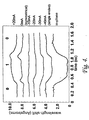
- Figure 4 illustrates how, in respect of a particular example of laser constructed as depicted in Figure 3, the varying of the degree of modulation depth asymmetry in the absence of any temporal asymmetry affects the chirp present in its output when modulated with the bit sequence '0, 1, 0'.
- the traces of Figure 4 were obtained by applying a constant current to terminal 38b of the laser, and switching the current applied to the terminal 38c, arbitrarily designating this as the terminal of terminals 38a and 38c nearer the output facet, between 0mA and 40mA.
- the different traces were produced by applying different values of current to terminal 38a, the terminal remote from the output facet.
- the current applied to terminal 38a was 40mA applied in phase with that applied to terminal 38c.
- the current applied to terminal 38a is applied in antiphase with respect to the application of the current to terminal 38c.
- the labelling of the traces, other than the 'in phase' trace, is in respect of asymmetry.
- the current applied to terminal 38a was switched between 40mA and 0mA.
- the current applied to the terminal 38a was switched between 0mA and 0mA, i.e. the current drive was single ended. From considerations of symmetry one would have expected the 0mA trace to have been the flattest: the fact that the -10mA trace turns out to be flatter implies some departure from perfect physical symmetry of the specific laser under test.
- Figure 5 shows the simulated results in respect of different amounts of temporal asymmetry in the application of push-pull current drive applied to a laser constructed as depicted in Figure 3. This simulation was in respect of modulation at 1.5 Gb/s with a '0,1,0' bit sequence with a d.c. bias on contact 38b of 50mA, a d.c. bias of 22.5mA on each end contact 38a and 38c, and a modulation depth of 40mA on the end contacts.
- the simulation was based on the tme domain modelling as described by C F Tsang et al, "Comparison between 'power matrix model (PMM)' and 'time domain model (TDM)' in modeling large signal responses of DFB lasers," IEE Proc. J vol. 141, no. 2, pp 89-96, Apr. 1994, and by L M Zhang et al, "Dynamic analysis of radiation and side mode suppression in second order DFB lasers using time-domain large signal travelling wave model," IEEE J. Quantum Electron., vol. 30, no. 6, pp. 1389-1395, June 1994.
- a pulse is turned on by switching off the contact further from the output and switching on the contact nearer the output.
- the switching off of the more remote contact leads the switching on of the nearer contact, and so as a pulse turns on there is a transient decrease in mean carrier density and stored energy before the nearer contact is turned on.
- Such a transient decrease is associated with a transient positive emission wavelength shift.
- the switching on of the more remote contact leads the switching off of the nearer contact, and so at this juncture there is a transient increase in mean carrier density and stored energy, such a transient being associated with a transient negative emission wavelength shift.
- the effects are interchanged in the change of a negative temporal asymmetry because in this instance an increase in mean carrier density and stored energy is associated with turn on and a decrease with turn off.
- Figure 6 shows a further trace in which the temporal asymmetry was +60ps, but this time in the presence of a bias level asymmetry of +10mA.
- Figure 7 shows how the extinction ratio varies with temporal asymmetry using the same drive conditions as described above with reference to Figure 5. This shows that the offset does not significantly affect extinction ratio.
- Figure 8 shows the eye diagrams
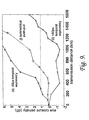
- Figure 9 shows the effect on the eye closure plot when positive and negative temporal asymmetry are applied in the manner described above with reference to Figure 5 using a +60ps temporal asymmetry.
- positive temporal asymmetry results in very strong pulse compression and can significantly improve the transmission distance to beyond 1200km for a 1 dB eye closure
- negative temporal asymmetry causes the eye to close more rapidly.
- the red and blue wavelength shifts at the leading and trailing edges of the pulse cause the edges to move together as the pulse propagates, giving strong compression similar to that which occurs for a negative chirp external modulator.
- the opposite occurs when a negative temporal asymmetry is applied and the edges rapidly spread apart.
- the use of temporal asymmetry therefore affords the opportunity for transmission performance comparable with that of a negative chirp external modulator.
- optimisation of the chirp will depend on the laser structure and the dispersion in the fibre link. An important point is that it is not necessarily the lowest level of chirp which will provide the best performance; rather it is the shape of the time resolved chirp which is important.
- Push-pull modulation offers the potential to tailor this shape, and a comparison can be made with an external modulator.
- An external modulator can allow a pulse to be 'pre-chirped', i.e. the spectral shape is tailored to compensate for a given dispersion in a fibre. With appropriate biasing, an external modulator can provide negative chirp allowing large transmission spans.
- the chirp can be tailored to provide a pre-chirped pulse to compensate for dispersion, and with appropriate temporal asymmetry a negative chirp shape similar to that obtained from an optimised external modulator can be obtained, but with the advantages of cost and simplicity offered by a directly modulated source.
Landscapes
- Physics & Mathematics (AREA)
- Condensed Matter Physics & Semiconductors (AREA)
- General Physics & Mathematics (AREA)
- Electromagnetism (AREA)
- Optics & Photonics (AREA)
- Optical Communication System (AREA)
- Semiconductor Lasers (AREA)
Description
- This invention relates to the control of chirp in high speed amplitude modulation of DFB lasers.
- Modulation of the injection current of a semiconductor distributed feedback (DFB) laser is liable to produce variation in both the intensity and the wavelength of its emission. This wavelength variation is called chirp. Chirp imposes bandwidth limitations in amplitude modulated transmission systems that exhibit wavelength dispersion.
- A paper entitled 'Independent modulation in amplitude and frequency regimes by a multi-electrode distributed - feedback laser' presented by Y Yoshikuni et al at the February 25 1986 Optical Fiber Communication Conference in Atlanta, Georgia describes a DFB laser with a uniform physical pitch grating where the top electrode of the laser is divided into three in-line sections, at least one of which is driven independently of the others. In particular, the paper states that differences in modulation efficiencies make it possible to modulate amplitude and frequency independently by adjusting the modulation current amplitude and phase applied to the divided electrode structure, and illustrates achieving amplitude modulation with minimum chirp by applying a first signal to the front portion of the divided electrode slightly ahead in phase of the application of a second signal of smaller amplitude to the centre portion of the divided electrode structure. Correspondingly frequency modulation with minimum amplitude modulation is described as being achieved with the first current being of larger amplitude than the second and in substantial antiphase (push-pull) relationship.
- A paper by O Nilsson et al entitled, 'Formulas for Direct Frequency Modulation Response of Two-Electrode Diode Lasers: Proposals for Improvement', Electronics Letters 3rd December 1987,
Vol 23,No 25, pages 1371-2 describes the theory of operation of a two-electrode laser structure designed for frequency modulation rather than for amplitude modulation. According to this theory thermal effects produce a phase shift, but it is postulated that the thermal effect could be avoided by pumping the laser in push pull. It is however particularly to be noted that this push-pull operation of a two-electrode laser is in the context of a device structured to provide frequency modulation rather than amplitude modulation, and the paper explains that the two sections are required to have different α-parameters in order to provide the desired frequency modulation. Thus it is clear that this suggestion to employ push-pull is specifically in respect of a laser diode that is not symmetrical about the plane separating the two sections of that laser. - Neither of the above referenced papers is however directly concerned with dynamic chirp, by which term is meant the transient effects upon emission frequency occurring at the rising and falling edges of fast pulses. As the data rate is increased so this dynamic chirp assumes greater significance as a potential problem. Dynamic chirp is believed to result in major part from the effect of changes in total photon population in the laser associated with the rising and falling edges of the injection modulation current, and so the elimination of a frequency modulation response to injection current modulation in the manner proposed in the above references does not address the particular problem of dynamic chirp.
- A paper that does address this dynamic chirp problem is the paper by I H White et al entitled 'Line Narrowed Picosecond Optical Pulse Generation Using Three Contact InGaAsP/InP multi-quantum Well distributed Feedback Laser under Gain Switching', Electronics Letters Vol. 28,
No 13, pages 1257-8. As the title implies, the laser has a three section top electrode, of which the two end sections are electrically commoned. Dynamic chirp is reduced by arranging to gain-switch the commoned end sections while a constant bias is applied to the middle section in such a way as to provide an effective optical injection locking mechanism. The central region causes locking of the wavelength of gain-switched pulses generated by the electrical modulation applied to the end regions. This reduces chirp, but insofar as it still leaves a modulation of the photon population, the approach is not fully effective. - United States Patent No. 5 502 741 is directed to the control of chirp and describes a method of amplitude modulating the optical emission of a DFB laser in such a way as to minimise dynamic chirp. To this end a DFB laser is provided with a top electrode divided symmetrically into two or three in-line separate elements through which a bias current is applied with a symmetrical distribution and through which a modulation current is applied with an antisymmetric (push-pull) distribution.
- The present invention particularly relates to the provision of a method of amplitude modulating the optical emission of a DFB laser in such a way as to optimise dynamic chirp. Typically the DFB laser will be at the transmitter end of an optical transmission system, and optimised chirp will be the chirp that provides minimised eye closure penalty at the receiver end. Generally this optimised chirp condition will not be the same as the condition providing minimised dynamic chirp in the output from the DFB laser.
- According to the present invention as defined in
claim 1 there is provided a method of amplitude modulating a distributed feedback (DFB) injection laser whose optical cavity has a plane of substantial symmetry normal to the optical emission axis of the laser, in which method a bias current, which is distributed substantially symmetrically with respect to said plane of substantial symmetry is applied to the DFB optical cavity, upon which bias current is superimposed a modulation current that consists of data and inverse data components, wherein the data component has a distribution that is asymmetrically weighted with respect to the plane of substantial symmetry and the inverse data component has a distribution that is a replica of the data component, wherein the data and inverse data components are applied with mirror symmetry with respect to the plane of substantial symmetry, characterised in that the data component is applied in phase-shifted relationship with respect to the application of the inverse data component so that the components operate in phase-shifted push-pull mode in order to optimise the dynamic chirp. - The data and inverse data components of the modulation current are not necessarily of equal amplitude.
- The invention as defined in
claim 3 also provides a distributed feedback (DFB) injection laser provided with an electrode structure by means of which current can be injected into the DFB laser's optical cavity to cause the laser to lase, wherein said structure is a divided structure that permits the current injection to be established with a distribution along the optical emission axis of the laser's optical cavity that can be varied, wherein the optical cavity has a plane of substantial symmetry normal to the optical emission axis, which DFB laser is provided with drive means adapted to apply to the divided electrode structure a bias current disposed symmetrically with respect to the plane of substantial symmetry, to superimpose upon said bias current a modulation current that consists of data and inverse data components, wherein the data component has a distribution that is asymmetrically weighted with respect to the plane of substantial symmetry and the inverse data component has a distribution that is a replica of the data component, and to apply the data and inverse data components with mirror symmetry with respect to the plane of substantial symmetry, which drive means is characterised in that it is adapted to apply the data component in phase-shifted relationship with respect to its application of the inverse data component so that the components operate in phase-shifted push-pull mode in order to optimise the dynamic chirp. - The invention as defined in
claim 5 further resides in an optical transmission system incorporating a laser as set out in the preceding paragraph. - There follows a description of lasers, for use in optical transmission systems, and their modes of operation embodying the invention in preferred forms. In this description reference is made to the accompanying drawings in which:-
- Figure 1
- schematically depicts an optical transmission system,
- Figures 2 and 3
- depict schematic longitudinal sections respectively of two-section and three-section top electrode DFB lasers,
- Figure 4
- is a set of plots illustrating the chirp for different levels of amplitude asymmetry in the laser drive,
- Figure 5
- is a set of plots illustrating the chirp for different levels of temporal asymmetry in the laser drive,
- Figure 6
- is a further plot illustrating the chirp for a specific value of temporal asymmetry with d.c. bias asymmetry,
- Figure 7
- is a plot illustrating the variation in extinction ratio with temporal asymmetry in the laser drive, and
- Figures 8A and 8B
- are simulated eye diagrams respectively for positive and negative temporal asymmetry, and
- Figure 9
- depicts plots of eye closure against transmission distance for different amounts of temporal assymetry.
- The basic elements of an optical transmission system are depicted in Figure 1, and comprise a
transmitter 10 optically coupled with anoptical receiver 11 by means of atransmission path 12. Typically that transmission path may include a concatenation ofoptical amplifiers 13. In this instance thetransmitter 10 includes at least one directly modulated DFB semiconductor laser (not separately illustrated in Figure 1) and, in the case of a transmitter for a wavelength division multiplexed transmission system, will contain more than one of such lasers. - A preferred form of basic semiconductor structure of DFB laser to which the method of amplitude modulation according to the present invention is applied is a conventional DFB laser structure with the single major difference that preferably the distributed feedback grating is without any phase shift. Such a basic semiconductor structure may for instance comprise, as depicted in Figure 2, an n-
type InP substrate 20 upon which is grown a series of epitaxially deposited layers commencing with an n-typeInP buffer layer 21. On top of the buffer layer is grown an undoped quaternarylower waveguide layer 22, a multi-quantum well (MQW)structure 23, an undoped quaternaryupper waveguide layer 24, a p-typeInP cladding layer 25 and a p-typeternary contact layer 26. - The
MQW structure 23 may typically comprise about six quantum strained or unstrained well layers of ternary or quaternary material sandwiched between barrier layers which may have the same composition as that of the upper andlower waveguide layers layers buffer layer 21. - The above described layer structure provides waveguiding properties in the direction normal to the plane of the layers. Lateral waveguiding is also provided by known means, for instance by means of a ridge waveguide structure or by means of a buried heterostructure structure, and in this way an optical axis for the laser is defined, this axis extending in the plane of the layer in a direction at right angles to the direction in which the grating lines of the DFB
structure 27 extend. Usually a DFB laser has a single top electrode making electrical contact with thecontact layer 26, but in this instance the top electrode is divided into two in-line sections 28a, 28b as depicted in Figure 2 or three in-line sections - The arrangement of the top electrode sections is such as to retain a plane of substantial symmetry (indicated by a
broken line 29, 39) for the semiconductor laser structure and its electrode structure. The laser is thus provided with a structure that confines the photons laterally and perpendicular to the plane of the epitaxial layers, and now by means of the divided top electrode structure is provided with a facility for modulating the distribution of the photons along the optical axis of the laser by modulation of the distribution of the injection current applied to the laser via its top electrode structure. In accordance with the teachings of US Patent No. 5 502 741, the laser is supplied with a bias current that is distributed substantially symmetrically with respect to thesymmetry plane respective elements 28a and 28b, currents of the form (ib ± im) and (ib ∓ im), where ib is the bias current and im is the modulation current. (For the sake of illustration, under the condition ib = im, the total current drive would alternate between application solely through element 28d and application solely through element 28b). In the case of the three-element top electrode configuration of Figure 3, the required symmetry relationships are provided by applying, to therespective elements - According to the teachings of the present invention, the bias current is applied in the same way, but the modulation current is applied with a phase difference between the application of ± im to terminal 28a or 38a and the application of ∓ im to terminal 28b or 38b. In the case of a laser structure with a more complex top electrode structure in which the current ± im is not applied in its entirety to a single electrode, but is distributed between two or more electrodes, this distribution needs to be asymmetrically weighted with respect to the plane of
symmetry - Additional to the asymmetry of drive conditions produced by the existence of a phase difference between the application of ± im and ∓ im, there may also be an asymmetry in the relative amplitudes of the two drive currents so as to provide ± kim and ∓ im, where k is a constant differing from unity. In order to distinguish clearly between these two forms of asymmetry, the asymmetry introduced by differences in relative amplitudes of the modulation current will be termed modulation depth asymmetry, while that produced by differences in their phases will be termed temporal asymmetry. To discuss these effects it is convenient to adopt a convention to define what is meant by positive and negative in respect of both these types of asymmetry. Accordingly, positive modulation depth asymmetry is defined as the condition in which the modulation depth on the side of the plane of symmetry remote from the output facet of the laser exceeds that on the nearer side. Thus under conditions of positive modulation depth asymmetry the energy stored in the laser decreases as a pulse turns the laser on. Positive temporal asymmetry is defined as the condition in which the modulation applied on the side of the plane of symmetry remote from the output facet of the laser is applied in advance of that applied on the nearer side.
- Figure 4 illustrates how, in respect of a particular example of laser constructed as depicted in Figure 3, the varying of the degree of modulation depth asymmetry in the absence of any temporal asymmetry affects the chirp present in its output when modulated with the bit sequence '0, 1, 0'. The traces of Figure 4 were obtained by applying a constant current to terminal 38b of the laser, and switching the current applied to the terminal 38c, arbitrarily designating this as the terminal of
terminals - Attention is now turned to the effects of temporal drive asymmetry. Figure 5 shows the simulated results in respect of different amounts of temporal asymmetry in the application of push-pull current drive applied to a laser constructed as depicted in Figure 3. This simulation was in respect of modulation at 1.5 Gb/s with a '0,1,0' bit sequence with a d.c. bias on contact 38b of 50mA, a d.c. bias of 22.5mA on each
end contact data 1 matches that in the body of adata 0. - This effect can be understood by considering the change in stored energy and mean carrier density. A pulse is turned on by switching off the contact further from the output and switching on the contact nearer the output. For a positive temporal asymmetry, the switching off of the more remote contact leads the switching on of the nearer contact, and so as a pulse turns on there is a transient decrease in mean carrier density and stored energy before the nearer contact is turned on. Such a transient decrease is associated with a transient positive emission wavelength shift.
- At the turn off, the switching on of the more remote contact leads the switching off of the nearer contact, and so at this juncture there is a transient increase in mean carrier density and stored energy, such a transient being associated with a transient negative emission wavelength shift. The effects are interchanged in the change of a negative temporal asymmetry because in this instance an increase in mean carrier density and stored energy is associated with turn on and a decrease with turn off.
- Figure 6 shows a further trace in which the temporal asymmetry was +60ps, but this time in the presence of a bias level asymmetry of +10mA.
- Figure 7 shows how the extinction ratio varies with temporal asymmetry using the same drive conditions as described above with reference to Figure 5. This shows that the offset does not significantly affect extinction ratio.
- Figure 8 shows the eye diagrams, and Figure 9 shows the effect on the eye closure plot when positive and negative temporal asymmetry are applied in the manner described above with reference to Figure 5 using a +60ps temporal asymmetry. It can be seen that positive temporal asymmetry results in very strong pulse compression and can significantly improve the transmission distance to beyond 1200km for a 1 dB eye closure, whereas negative temporal asymmetry causes the eye to close more rapidly. This can be explained by considering the time resolved chirp shapes. The red and blue wavelength shifts at the leading and trailing edges of the pulse cause the edges to move together as the pulse propagates, giving strong compression similar to that which occurs for a negative chirp external modulator. The opposite occurs when a negative temporal asymmetry is applied and the edges rapidly spread apart. The use of temporal asymmetry therefore affords the opportunity for transmission performance comparable with that of a negative chirp external modulator.
- The precise form of optimisation of the chirp will depend on the laser structure and the dispersion in the fibre link. An important point is that it is not necessarily the lowest level of chirp which will provide the best performance; rather it is the shape of the time resolved chirp which is important. Push-pull modulation offers the potential to tailor this shape, and a comparison can be made with an external modulator. An external modulator can allow a pulse to be 'pre-chirped', i.e. the spectral shape is tailored to compensate for a given dispersion in a fibre. With appropriate biasing, an external modulator can provide negative chirp allowing large transmission spans. Similarly, with push-pull modulation, the chirp can be tailored to provide a pre-chirped pulse to compensate for dispersion, and with appropriate temporal asymmetry a negative chirp shape similar to that obtained from an optimised external modulator can be obtained, but with the advantages of cost and simplicity offered by a directly modulated source.
Claims (5)
- A method of amplitude modulating a distributed feedback (DFB) injection laser whose optical cavity has a plane of substantial symmetry (29, 39) normal to the optical emission axis of the laser, in which method a bias current, which is distributed substantially symmetrically with respect to said plane of substantial symmetry is applied to the DFB optical cavity, upon which bias current is superimposed a modulation current that consists of data and inverse data components, wherein the data component has a distribution that is asymmetrically weighted with respect to the plane of substantial symmetry and the inverse data component has a distribution that is a replica of the data component, wherein the data and inverse data components are applied with mirror symmetry with respect to the plane of substantial symmetry, characterised in that the data component is applied in phase-shifted relationship with respect to the application of the inverse data component so that the components operate in phase-shifted push-pull mode in order to optimise the dynamic chirp
- A method as claimed in claim 1, wherein the inverse component that is a replica of the data component has the same amplitude as the data component.
- A distributed feedback (DFB) injection laser provided with an electrode structure (28a, 28b; 38a, 38b, 38c) by means of which current can be injected into the DFB laser's optical cavity to cause the laser to lase, wherein said structure is a divided structure that permits the current injection to be established with a distribution along the optical emission axis of the laser's optical cavity that can be varied, wherein the optical cavity has a plane of substantial symmetry (29. 39) normal to the optical emission axis, which DFB laser is provided with drive means adapted to apply to the divided electrode structure a bias current disposed symmetrically with respect to the plane of substantial symmetry, to superimpose upon said bias current a modulation current that consists of data and inverse data components, wherein the data component has a distribution that is asymmetrically weighted with respect to the plane of substantial symmetry and the inverse data component has a distribution that is a replica of the data component, and to apply the data and inverse data components with mirror symmetry with respect to the plane of substantial symmetry, which drive means is characterised in that it is adapted to apply the data component in phase-shifted relationship with respect to its application of the inverse data component so that the components operate in phase-shifted push-pull mode in order to optimise the dynamic chirp.
- A DFB laser as claimed in claim 3, wherein the modulation current that the drive means is adapted to apply to the divided electrode structure has data and inverse data components of equal amplitude.
- An optical transmission system having an optical receiver (11) optically coupled via a transmission path (12) with an optical transmitter (10) that includes a DFB laser as claimed in claim 3 or 4.
Applications Claiming Priority (2)
| Application Number | Priority Date | Filing Date | Title |
|---|---|---|---|
| US865760 | 1997-05-30 | ||
| US08/865,760 US5901164A (en) | 1997-05-30 | 1997-05-30 | Direct amplitude modulation of lasers |
Publications (3)
| Publication Number | Publication Date |
|---|---|
| EP0881726A2 EP0881726A2 (en) | 1998-12-02 |
| EP0881726A3 EP0881726A3 (en) | 2000-06-28 |
| EP0881726B1 true EP0881726B1 (en) | 2004-06-16 |
Family
ID=25346168
Family Applications (1)
| Application Number | Title | Priority Date | Filing Date |
|---|---|---|---|
| EP98303274A Expired - Lifetime EP0881726B1 (en) | 1997-05-30 | 1998-04-28 | Direct amplitude modulation of lasers |
Country Status (5)
| Country | Link |
|---|---|
| US (1) | US5901164A (en) |
| EP (1) | EP0881726B1 (en) |
| JP (1) | JPH1174600A (en) |
| CA (1) | CA2235179A1 (en) |
| DE (1) | DE69824485T2 (en) |
Families Citing this family (6)
| Publication number | Priority date | Publication date | Assignee | Title |
|---|---|---|---|---|
| EP1085625A4 (en) * | 1999-03-31 | 2005-11-16 | Nat Inst Of Advanced Ind Scien | OPTICAL SURFACE AMPLIFIER AND METHOD FOR PRODUCING THE SAME |
| US6647048B2 (en) * | 2000-04-28 | 2003-11-11 | Photodigm, Inc. | Grating-outcoupled surface-emitting lasers using quantum wells with thickness and composition variation |
| US6714575B2 (en) * | 2001-03-05 | 2004-03-30 | Photodigm, Inc. | Optical modulator system |
| KR100429531B1 (en) * | 2001-10-12 | 2004-05-03 | 삼성전자주식회사 | Distributed feedback semiconductor laser |
| US8265112B2 (en) * | 2009-03-26 | 2012-09-11 | Kaiam Corp. | Semiconductor laser device and circuit for and method of driving same |
| JP7206393B2 (en) * | 2019-01-04 | 2023-01-17 | 華為技術有限公司 | Semiconductor lasers, optical transmission components, optical line terminals and optical network units |
Family Cites Families (1)
| Publication number | Priority date | Publication date | Assignee | Title |
|---|---|---|---|---|
| US5502741A (en) * | 1994-03-22 | 1996-03-26 | Northern Telecom Limited | Direct amplitude modulation of lasers |
-
1997
- 1997-05-30 US US08/865,760 patent/US5901164A/en not_active Expired - Lifetime
-
1998
- 1998-04-28 EP EP98303274A patent/EP0881726B1/en not_active Expired - Lifetime
- 1998-04-28 DE DE69824485T patent/DE69824485T2/en not_active Expired - Fee Related
- 1998-05-12 CA CA002235179A patent/CA2235179A1/en not_active Abandoned
- 1998-05-27 JP JP10146072A patent/JPH1174600A/en active Pending
Also Published As
| Publication number | Publication date |
|---|---|
| US5901164A (en) | 1999-05-04 |
| DE69824485T2 (en) | 2005-08-04 |
| EP0881726A2 (en) | 1998-12-02 |
| JPH1174600A (en) | 1999-03-16 |
| DE69824485D1 (en) | 2004-07-22 |
| EP0881726A3 (en) | 2000-06-28 |
| CA2235179A1 (en) | 1998-11-30 |
Similar Documents
| Publication | Publication Date | Title |
|---|---|---|
| US5784183A (en) | Semiconductor optical device and method for fabricating the same | |
| US5680411A (en) | Integrated monolithic laser-modulator component with multiple quantum well structure | |
| US6031851A (en) | Mode-locked semiconductor laser and method of driving the same | |
| EP0668641B1 (en) | Oscillation polarization mode selective semiconductor laser, light transmitter and optical communication system using the laser | |
| US6281030B1 (en) | Fabrication of semiconductor Mach-Zehnder modulator | |
| CA1242518A (en) | Frequency-stabilized semiconductor laser oscillator | |
| US20100260220A1 (en) | Semiconductor laser device and circuit for and method of driving same | |
| US5808314A (en) | Semiconductor emission device with fast wavelength modulation | |
| US5502741A (en) | Direct amplitude modulation of lasers | |
| JP3244976B2 (en) | Semiconductor laser driving method, semiconductor laser device, optical communication method, node, and optical communication system | |
| US5790581A (en) | Oscillation polarization mode selective semiconductor laser, light transmitter and optical communication system using the laser | |
| CA2410964C (en) | High-power, manufacturable sampled grating distributed bragg reflector lasers | |
| JPS63287088A (en) | Driving method of distributed feedback type laser and optical equipment and transmitter containing distributed feedback type laser | |
| US6526075B2 (en) | Method for driving a semiconductor light source device for transmitting a signal | |
| JP2002169131A (en) | Optical semiconductor device and method of modulating optical semiconductor device | |
| US5901164A (en) | Direct amplitude modulation of lasers | |
| US6091745A (en) | Semiconductor laser capable of changing polarization mode of its output light, semiconductor laser apparatus and driving method therefor | |
| US5073892A (en) | Semiconductor laser device | |
| JPH07231132A (en) | Semiconductor optical device | |
| Yamaguchi et al. | Semiconductor photonic integrated circuit for high-density WDM light source | |
| Otsubo et al. | Low-driving-current high-speed direct modulation up to 40 Gb/s using 1.3-μm semi-insulating buried-heterostructure AlGaInAs-MQW distributed reflector (DR) lasers | |
| WO2022033684A1 (en) | High speed modulated laser | |
| JP2889594B2 (en) | Semiconductor optical device and optical communication system | |
| JP3149944B2 (en) | Semiconductor laser and driving method thereof | |
| JPH05251818A (en) | Operating method for semiconductor laser as bistable photoelectric component |
Legal Events
| Date | Code | Title | Description |
|---|---|---|---|
| PUAI | Public reference made under article 153(3) epc to a published international application that has entered the european phase |
Free format text: ORIGINAL CODE: 0009012 |
|
| AK | Designated contracting states |
Kind code of ref document: A2 Designated state(s): DE FR GB IT SE |
|
| AX | Request for extension of the european patent |
Free format text: AL;LT;LV;MK;RO;SI |
|
| RIN1 | Information on inventor provided before grant (corrected) |
Inventor name: CARROLL, JOHN EDWARD Inventor name: FLANIGAN, BARRY JOHN |
|
| RAP3 | Party data changed (applicant data changed or rights of an application transferred) |
Owner name: NORTEL NETWORKS CORPORATION |
|
| PUAL | Search report despatched |
Free format text: ORIGINAL CODE: 0009013 |
|
| AK | Designated contracting states |
Kind code of ref document: A3 Designated state(s): AT BE CH CY DE DK ES FI FR GB GR IE IT LI LU MC NL PT SE |
|
| AX | Request for extension of the european patent |
Free format text: AL;LT;LV;MK;RO;SI |
|
| RAP1 | Party data changed (applicant data changed or rights of an application transferred) |
Owner name: NORTEL NETWORKS LIMITED |
|
| 17P | Request for examination filed |
Effective date: 20001228 |
|
| AKX | Designation fees paid |
Free format text: DE FR GB IT SE |
|
| RAP1 | Party data changed (applicant data changed or rights of an application transferred) |
Owner name: BOOKHAM TECHNOLOGY PLC |
|
| GRAP | Despatch of communication of intention to grant a patent |
Free format text: ORIGINAL CODE: EPIDOSNIGR1 |
|
| RIC1 | Information provided on ipc code assigned before grant |
Ipc: 7H 01S 5/06 A |
|
| RIC1 | Information provided on ipc code assigned before grant |
Ipc: 7H 01S 5/06 A |
|
| GRAS | Grant fee paid |
Free format text: ORIGINAL CODE: EPIDOSNIGR3 |
|
| GRAA | (expected) grant |
Free format text: ORIGINAL CODE: 0009210 |
|
| AK | Designated contracting states |
Kind code of ref document: B1 Designated state(s): DE FR GB IT SE |
|
| PG25 | Lapsed in a contracting state [announced via postgrant information from national office to epo] |
Ref country code: IT Free format text: LAPSE BECAUSE OF FAILURE TO SUBMIT A TRANSLATION OF THE DESCRIPTION OR TO PAY THE FEE WITHIN THE PRESCRIBED TIME-LIMIT;WARNING: LAPSES OF ITALIAN PATENTS WITH EFFECTIVE DATE BEFORE 2007 MAY HAVE OCCURRED AT ANY TIME BEFORE 2007. THE CORRECT EFFECTIVE DATE MAY BE DIFFERENT FROM THE ONE RECORDED. Effective date: 20040616 |
|
| REG | Reference to a national code |
Ref country code: GB Ref legal event code: FG4D |
|
| REF | Corresponds to: |
Ref document number: 69824485 Country of ref document: DE Date of ref document: 20040722 Kind code of ref document: P |
|
| PG25 | Lapsed in a contracting state [announced via postgrant information from national office to epo] |
Ref country code: SE Free format text: LAPSE BECAUSE OF FAILURE TO SUBMIT A TRANSLATION OF THE DESCRIPTION OR TO PAY THE FEE WITHIN THE PRESCRIBED TIME-LIMIT Effective date: 20040916 |
|
| 111Z | Information provided on other rights and legal means of execution |
Free format text: DEFRGBITSE Effective date: 20031030 |
|
| ET | Fr: translation filed | ||
| PLBE | No opposition filed within time limit |
Free format text: ORIGINAL CODE: 0009261 |
|
| STAA | Information on the status of an ep patent application or granted ep patent |
Free format text: STATUS: NO OPPOSITION FILED WITHIN TIME LIMIT |
|
| PGFP | Annual fee paid to national office [announced via postgrant information from national office to epo] |
Ref country code: GB Payment date: 20050427 Year of fee payment: 8 |
|
| 26N | No opposition filed |
Effective date: 20050317 |
|
| PG25 | Lapsed in a contracting state [announced via postgrant information from national office to epo] |
Ref country code: DE Free format text: LAPSE BECAUSE OF NON-PAYMENT OF DUE FEES Effective date: 20051101 |
|
| PG25 | Lapsed in a contracting state [announced via postgrant information from national office to epo] |
Ref country code: FR Free format text: LAPSE BECAUSE OF NON-PAYMENT OF DUE FEES Effective date: 20051230 |
|
| REG | Reference to a national code |
Ref country code: FR Ref legal event code: ST Effective date: 20051230 |
|
| PG25 | Lapsed in a contracting state [announced via postgrant information from national office to epo] |
Ref country code: GB Free format text: LAPSE BECAUSE OF NON-PAYMENT OF DUE FEES Effective date: 20060428 |
|
| GBPC | Gb: european patent ceased through non-payment of renewal fee |
Effective date: 20060428 |