EP0880036B1 - Method for altering the temperature dependence of optical waveguide devices - Google Patents
Method for altering the temperature dependence of optical waveguide devices Download PDFInfo
- Publication number
- EP0880036B1 EP0880036B1 EP98303701A EP98303701A EP0880036B1 EP 0880036 B1 EP0880036 B1 EP 0880036B1 EP 98303701 A EP98303701 A EP 98303701A EP 98303701 A EP98303701 A EP 98303701A EP 0880036 B1 EP0880036 B1 EP 0880036B1
- Authority
- EP
- European Patent Office
- Prior art keywords
- waveguide
- temperature
- glass
- optical
- compensating material
- Prior art date
- Legal status (The legal status is an assumption and is not a legal conclusion. Google has not performed a legal analysis and makes no representation as to the accuracy of the status listed.)
- Expired - Lifetime
Links
- 230000003287 optical effect Effects 0.000 title claims description 37
- 238000000034 method Methods 0.000 title claims description 18
- 239000011521 glass Substances 0.000 claims description 31
- 239000000463 material Substances 0.000 claims description 25
- XLYOFNOQVPJJNP-ZSJDYOACSA-N heavy water Substances [2H]O[2H] XLYOFNOQVPJJNP-ZSJDYOACSA-N 0.000 claims description 17
- 238000005253 cladding Methods 0.000 claims description 12
- 239000000758 substrate Substances 0.000 claims description 9
- OKKJLVBELUTLKV-UHFFFAOYSA-N Methanol Chemical compound OC OKKJLVBELUTLKV-UHFFFAOYSA-N 0.000 claims description 6
- 230000000873 masking effect Effects 0.000 claims description 6
- 239000013307 optical fiber Substances 0.000 claims description 6
- LFQSCWFLJHTTHZ-UHFFFAOYSA-N Ethanol Chemical compound CCO LFQSCWFLJHTTHZ-UHFFFAOYSA-N 0.000 claims description 4
- 230000000694 effects Effects 0.000 claims description 4
- 239000011248 coating agent Substances 0.000 claims description 2
- 238000000576 coating method Methods 0.000 claims description 2
- 230000002708 enhancing effect Effects 0.000 claims description 2
- 229910052751 metal Inorganic materials 0.000 claims description 2
- 239000002184 metal Substances 0.000 claims description 2
- 238000007789 sealing Methods 0.000 claims description 2
- 230000001747 exhibiting effect Effects 0.000 claims 1
- VYPSYNLAJGMNEJ-UHFFFAOYSA-N Silicium dioxide Chemical compound O=[Si]=O VYPSYNLAJGMNEJ-UHFFFAOYSA-N 0.000 description 18
- 239000000377 silicon dioxide Substances 0.000 description 9
- 239000000835 fiber Substances 0.000 description 7
- XUIMIQQOPSSXEZ-UHFFFAOYSA-N Silicon Chemical compound [Si] XUIMIQQOPSSXEZ-UHFFFAOYSA-N 0.000 description 6
- 229910052710 silicon Inorganic materials 0.000 description 6
- 239000010703 silicon Substances 0.000 description 6
- 230000008569 process Effects 0.000 description 5
- 239000010410 layer Substances 0.000 description 4
- 238000004519 manufacturing process Methods 0.000 description 4
- 229910052698 phosphorus Inorganic materials 0.000 description 4
- 230000035945 sensitivity Effects 0.000 description 4
- OAICVXFJPJFONN-UHFFFAOYSA-N Phosphorus Chemical compound [P] OAICVXFJPJFONN-UHFFFAOYSA-N 0.000 description 3
- 229910052796 boron Inorganic materials 0.000 description 3
- 230000008859 change Effects 0.000 description 3
- 230000001419 dependent effect Effects 0.000 description 3
- 239000011574 phosphorus Substances 0.000 description 3
- 230000009467 reduction Effects 0.000 description 3
- ZOXJGFHDIHLPTG-UHFFFAOYSA-N Boron Chemical compound [B] ZOXJGFHDIHLPTG-UHFFFAOYSA-N 0.000 description 2
- 230000004075 alteration Effects 0.000 description 2
- 230000005540 biological transmission Effects 0.000 description 2
- 238000010586 diagram Methods 0.000 description 2
- 229910052732 germanium Inorganic materials 0.000 description 2
- GNPVGFCGXDBREM-UHFFFAOYSA-N germanium atom Chemical compound [Ge] GNPVGFCGXDBREM-UHFFFAOYSA-N 0.000 description 2
- 230000001965 increasing effect Effects 0.000 description 2
- 238000004806 packaging method and process Methods 0.000 description 2
- VYZAMTAEIAYCRO-UHFFFAOYSA-N Chromium Chemical compound [Cr] VYZAMTAEIAYCRO-UHFFFAOYSA-N 0.000 description 1
- 229910052581 Si3N4 Inorganic materials 0.000 description 1
- 230000002411 adverse Effects 0.000 description 1
- 230000000903 blocking effect Effects 0.000 description 1
- 229910052804 chromium Inorganic materials 0.000 description 1
- 239000011651 chromium Substances 0.000 description 1
- 239000002131 composite material Substances 0.000 description 1
- 239000000470 constituent Substances 0.000 description 1
- 239000012792 core layer Substances 0.000 description 1
- 230000008878 coupling Effects 0.000 description 1
- 238000010168 coupling process Methods 0.000 description 1
- 238000005859 coupling reaction Methods 0.000 description 1
- 230000001934 delay Effects 0.000 description 1
- 238000000151 deposition Methods 0.000 description 1
- 239000006185 dispersion Substances 0.000 description 1
- 239000002019 doping agent Substances 0.000 description 1
- 238000005516 engineering process Methods 0.000 description 1
- 238000001914 filtration Methods 0.000 description 1
- PCHJSUWPFVWCPO-UHFFFAOYSA-N gold Chemical compound [Au] PCHJSUWPFVWCPO-UHFFFAOYSA-N 0.000 description 1
- 229910052737 gold Inorganic materials 0.000 description 1
- 239000010931 gold Substances 0.000 description 1
- 239000007788 liquid Substances 0.000 description 1
- 239000000203 mixture Substances 0.000 description 1
- 238000012544 monitoring process Methods 0.000 description 1
- 230000010363 phase shift Effects 0.000 description 1
- 238000005268 plasma chemical vapour deposition Methods 0.000 description 1
- 230000000644 propagated effect Effects 0.000 description 1
- 230000006798 recombination Effects 0.000 description 1
- 238000005215 recombination Methods 0.000 description 1
- 230000004044 response Effects 0.000 description 1
- 239000004065 semiconductor Substances 0.000 description 1
- 235000012239 silicon dioxide Nutrition 0.000 description 1
- HQVNEWCFYHHQES-UHFFFAOYSA-N silicon nitride Chemical compound N12[Si]34N5[Si]62N3[Si]51N64 HQVNEWCFYHHQES-UHFFFAOYSA-N 0.000 description 1
- 230000003595 spectral effect Effects 0.000 description 1
- 230000006641 stabilisation Effects 0.000 description 1
- 238000011105 stabilization Methods 0.000 description 1
- 230000002277 temperature effect Effects 0.000 description 1
- 230000008542 thermal sensitivity Effects 0.000 description 1
Images


Classifications
-
- G—PHYSICS
- G02—OPTICS
- G02B—OPTICAL ELEMENTS, SYSTEMS OR APPARATUS
- G02B6/00—Light guides; Structural details of arrangements comprising light guides and other optical elements, e.g. couplings
- G02B6/10—Light guides; Structural details of arrangements comprising light guides and other optical elements, e.g. couplings of the optical waveguide type
- G02B6/12—Light guides; Structural details of arrangements comprising light guides and other optical elements, e.g. couplings of the optical waveguide type of the integrated circuit kind
- G02B6/12007—Light guides; Structural details of arrangements comprising light guides and other optical elements, e.g. couplings of the optical waveguide type of the integrated circuit kind forming wavelength selective elements, e.g. multiplexer, demultiplexer
- G02B6/12009—Light guides; Structural details of arrangements comprising light guides and other optical elements, e.g. couplings of the optical waveguide type of the integrated circuit kind forming wavelength selective elements, e.g. multiplexer, demultiplexer comprising arrayed waveguide grating [AWG] devices, i.e. with a phased array of waveguides
- G02B6/12011—Light guides; Structural details of arrangements comprising light guides and other optical elements, e.g. couplings of the optical waveguide type of the integrated circuit kind forming wavelength selective elements, e.g. multiplexer, demultiplexer comprising arrayed waveguide grating [AWG] devices, i.e. with a phased array of waveguides characterised by the arrayed waveguides, e.g. comprising a filled groove in the array section
-
- G—PHYSICS
- G02—OPTICS
- G02B—OPTICAL ELEMENTS, SYSTEMS OR APPARATUS
- G02B6/00—Light guides; Structural details of arrangements comprising light guides and other optical elements, e.g. couplings
- G02B6/10—Light guides; Structural details of arrangements comprising light guides and other optical elements, e.g. couplings of the optical waveguide type
- G02B6/12—Light guides; Structural details of arrangements comprising light guides and other optical elements, e.g. couplings of the optical waveguide type of the integrated circuit kind
- G02B6/12007—Light guides; Structural details of arrangements comprising light guides and other optical elements, e.g. couplings of the optical waveguide type of the integrated circuit kind forming wavelength selective elements, e.g. multiplexer, demultiplexer
- G02B6/12009—Light guides; Structural details of arrangements comprising light guides and other optical elements, e.g. couplings of the optical waveguide type of the integrated circuit kind forming wavelength selective elements, e.g. multiplexer, demultiplexer comprising arrayed waveguide grating [AWG] devices, i.e. with a phased array of waveguides
- G02B6/12026—Light guides; Structural details of arrangements comprising light guides and other optical elements, e.g. couplings of the optical waveguide type of the integrated circuit kind forming wavelength selective elements, e.g. multiplexer, demultiplexer comprising arrayed waveguide grating [AWG] devices, i.e. with a phased array of waveguides characterised by means for reducing the temperature dependence
- G02B6/12028—Light guides; Structural details of arrangements comprising light guides and other optical elements, e.g. couplings of the optical waveguide type of the integrated circuit kind forming wavelength selective elements, e.g. multiplexer, demultiplexer comprising arrayed waveguide grating [AWG] devices, i.e. with a phased array of waveguides characterised by means for reducing the temperature dependence based on a combination of materials having a different refractive index temperature dependence, i.e. the materials are used for transmitting light
-
- G—PHYSICS
- G02—OPTICS
- G02B—OPTICAL ELEMENTS, SYSTEMS OR APPARATUS
- G02B6/00—Light guides; Structural details of arrangements comprising light guides and other optical elements, e.g. couplings
- G02B6/10—Light guides; Structural details of arrangements comprising light guides and other optical elements, e.g. couplings of the optical waveguide type
- G02B6/12—Light guides; Structural details of arrangements comprising light guides and other optical elements, e.g. couplings of the optical waveguide type of the integrated circuit kind
- G02B6/13—Integrated optical circuits characterised by the manufacturing method
-
- G—PHYSICS
- G02—OPTICS
- G02B—OPTICAL ELEMENTS, SYSTEMS OR APPARATUS
- G02B6/00—Light guides; Structural details of arrangements comprising light guides and other optical elements, e.g. couplings
- G02B6/24—Coupling light guides
- G02B6/26—Optical coupling means
- G02B6/28—Optical coupling means having data bus means, i.e. plural waveguides interconnected and providing an inherently bidirectional system by mixing and splitting signals
- G02B6/293—Optical coupling means having data bus means, i.e. plural waveguides interconnected and providing an inherently bidirectional system by mixing and splitting signals with wavelength selective means
- G02B6/29304—Optical coupling means having data bus means, i.e. plural waveguides interconnected and providing an inherently bidirectional system by mixing and splitting signals with wavelength selective means operating by diffraction, e.g. grating
- G02B6/29316—Light guides comprising a diffractive element, e.g. grating in or on the light guide such that diffracted light is confined in the light guide
- G02B6/29317—Light guides of the optical fibre type
-
- G—PHYSICS
- G02—OPTICS
- G02B—OPTICAL ELEMENTS, SYSTEMS OR APPARATUS
- G02B6/00—Light guides; Structural details of arrangements comprising light guides and other optical elements, e.g. couplings
- G02B6/24—Coupling light guides
- G02B6/26—Optical coupling means
- G02B6/28—Optical coupling means having data bus means, i.e. plural waveguides interconnected and providing an inherently bidirectional system by mixing and splitting signals
- G02B6/293—Optical coupling means having data bus means, i.e. plural waveguides interconnected and providing an inherently bidirectional system by mixing and splitting signals with wavelength selective means
- G02B6/29379—Optical coupling means having data bus means, i.e. plural waveguides interconnected and providing an inherently bidirectional system by mixing and splitting signals with wavelength selective means characterised by the function or use of the complete device
- G02B6/29398—Temperature insensitivity
Definitions
- broadband optical multiplexers are needed for delivering voice and video signals to the home, for combining pump and communications signals in an optical amplifier, and for adding monitoring signals to optical fibers.
- Dense wavelength-division multiplexing (WDM) systems need multiplexers to combine and separate channels of different wavelengths and need add-drop filters to alter the traffic.
- Low speed optical switches are needed for network reconfiguration.
- optical waveguide devices such as integrated optical silica waveguide circuits formed on planar silicon substrates.
- Such waveguides are typically formed by depositing base, core and cladding layers on a silicon substrate.
- the base layer can be made of undoped silica. It isolates the fundamental optical mode from the silicon substrate and thereby prevents optical loss at the silica substrate interface.
- the core layer is typically silica doped with phosphorus or germanium to increase its refractive index and thereby achieve optical confinement.
- the cladding is typically silica doped with both boron and phosphorus to facilitate fabrication and provide an index matching that of the base.
- the cores can be economically configured into a wide variety of compact configurations capable of performing useful functions. See, for example, Y.P. Li and C.H. Henry, "Silicon Optical Bench Waveguide Technology", Ch. 8, Optical Fiber Telecommunications, Vol. IIIB, p. 319-375 (Academic Press, 1997).
- Optical fibers typically comprise a higher index core, which can be doped silica, and a surrounding cladding of a lower index glass.
- a variety of all-fiber devices are made by providing one or more Bragg gratings in the fiber core. Such gratings are conventionally made by providing the core with a photosensitive dopant such as germanium and side-writing a grating using ultraviolet light.
- optical waveguide devices are based upon optical interference between beams of light propagated down different paths. Depending on the phase relationship between the beams at the point of recombination, light will either be transmitted or reflected back. Spectrally narrow, high contrast resonances can be readily designed, enabling high performance wavelength division multiplexers and blocking filters.
- variable ambient temperature has a perceptible and disadvantageous effect on the performance of such devices.
- the refractive index of the composite glass structure through which the light travels depends on temperature. Thus the spectral positions of critical resonances shift with temperature.
- Bragg gratings are critically dependent on the path lengths between successive index perturbations. But these path lengths change due to the temperature dependence of the refractive index, shifting the operating wavelength of the gratings.
- an optical waveguide device as claimed in claim 7.
- Glass waveguide devices are provided with enhanced temperature stability by incorporating within appropriate lengths of the waveguides a transparent compensating material having a refractive index variation with temperature that differs substantially from that of the waveguide.
- the compensating material a non-glass material, such as a liquid, driven into the glass by heat and pressure.
- D 2 O is incorporated into waveguides for optical communications.
- the D 2 O is transparent to the preferred communications wavelengths centered at about 1.55 ⁇ m and has a dn/dT opposite in polarity to the dn/dT of glass.
- the resulting structure exhibits enhanced temperature stability with reduced magnitude of dn/dT.
- the technique is particularly useful in devices based on interference between multiple waveguides, as it is not necessary to reduce dn/dT to zero in the respective waveguides. It suffices to compensate the differences. Such compensation can be achieved by compensating materials having dn/dT of either the same polarity as the dn/dT of the waveguides or the opposite polarity.
- Preferred embodiments include routers, Fourier filters and Bragg filters. In single waveguide devices such as gratings, compensating materials of opposite polarity can substantially enhance the temperature stability.
- Fig. 1 is a block diagram of the steps involved in enhancing the thermal stability of a waveguide device.
- the first step as illustrated in block A, is to provide a glass waveguide device to be improved.
- the waveguide device can be either a planar waveguide device, a fiber waveguide device or a combination of the two.
- Exemplary devices include routers, Fourier filters and Bragg gratings.
- Fig. 2A is a cross sectional view of an exemplary waveguide device (here a planar device) comprising a substrate 10, such as silicon, a base layer 11, such as undoped silica, one or more waveguide defined by one or more cores 12, 13, 14 and a cladding 15.
- the cladding can be doped with boron and phosphorus to achieve both a lowered flow temperature and an index preferably equal to the base layer.
- Fig. 2B is a plan view of the device of Fig. 2A.
- the cores 12, 13, 14 define optical waveguides of different lengths that extend between a common input 15 and a common output 16. Variations in temperature will produce different absolute thermal pathlength changes in the two waveguides.
- the methods for fabricating such waveguides are well known in the art and are described in further detail in C.H. Henry et al. "Glass Waveguides on Silicon for Hybrid Optical Packaging, J. Lightwave Technol. , 1539 (1989).
- the next step is to mask the waveguide, leaving exposed those regions where the refractive index variation with temperature (dn/dT) is to be altered. Where dn/dT is to be altered for the full length of the waveguide, masking is not required. But in applications where it is desired to equalize the effect of temperature variation among plural waveguides, different length waveguides will generally require masking to provide exposed regions of different length.
- the masking material should be impermeable to the treatment material. Silicon nitride films having a thickness on the order of 1 ⁇ m is preferred for masking devices to be treated with D 2 O. Such films can be deposited by plasma CVD.
- the third step (Fig. 1, block C) is to incorporate into the exposed regions of the waveguides a thermal compensating material which is transparent to the operating wavelength and which has a dn/dT different from that of the waveguide material.
- Typical waveguide glasses have a positive dn/dT, so the material incorporated into glass should have a negative dn/dT or a positive dn/dT substantially different from that of glass.
- Suitable negative dn/dT compensating materials include D 2 O, ethanol and methanol. The amount of material should exceed 1 weight percent of the glass and preferably should exceed 10%. D 2 O is preferred for glass communications devices operating at 1.55 ⁇ m.
- D 2 O can be incorporated in glass by exposing the glass to D 2 O steam at elevated temperature (100-300° C) and pressure 1-103 bar (15-1500 psi) for a period typically 1-20 hr.
- Fig. 2C shows the device of Fig. 2B after treatment with D 2 O in an exposed region such as triangle 20.
- Waveguide 12 is not exposed.
- Longer waveguide 13 is exposed over a first length, and the longest waveguide 14 is exposed over a second length longer than the first.
- the resulting device has enhanced temperature stability.
- the constitutive waveguides are processed so that their optical pathlengths are affected equally by changes in temperature.
- a compensating material having a positive dn/dT greater than glass were used, then the shorter waveguides would be treated over longer lengths to achieve compensation.
- the final steps are to remove the mask (block D) and to seal the incorporated material into the glass (block E). Sealing can be done by applying a thin coating of metal such as a few hundred nanometers of chromium or gold over the treated region 20.
- Sample 1 is a 2 cm length planar waveguide treated with D 2 O at 300° C for 15 hrs.
- Sample 2 is a 2 cm length of similar, untreated planar waveguide. 1.5 micrometer laser light was launched into each of the two samples and the temperature was raised approximately 40° C from room temperature to about 62° C. The interference between the front (entrance face) and back (exit face) reflections were monitored.
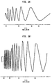
- Fig. 3A shows the interference fringes plotted against temperature for the treated sample and Fig 3B shows the infringes for the untreated sample. As can be seen, the treated sample has fewer fringes corresponding to a lower magnitude dn/dT.
- the magnitude of dn/dT for the treated sample is 9/16 that of the untreated sample for an enhancement factor e ⁇ 0.56 (56%).
- the process of Fig. 1 permits the fabrication of a wide variety of glass waveguide devices with enhanced temperature stability.
- the device is fabricated in the usual fashion, and the process of Fig. 1 is then applied after fabrication to alter the temperature coefficient of refractive index for one or more of the glass waveguides.
- this alteration can be applied in a spatially selective manner to equalize the temperature effects on different waveguides and thereby making the overall device temperature insensitive.
- the reduction in temperature sensitivity is proportional to minimization of dn/dT.
- Three important device applications will be illustrated: 1) temperature compensation of a multiwaveguide router, 2) temperature compensation of a multiwaveguide filter, and 3) reduction in temperature dependence of a single waveguide Bragg grating.
- Fig. 4 schematically illustrates an improved form of a device known as a waveguide grating router.
- the conventional portion of the device 40 comprises a pair of star couplers 41, 42 connected by an array 43 of waveguides that act like a grating, specifically there is a constant pathlength difference between adjacent waveguides in the array.
- the two star couplers 41, 42 are mirror images, except the number of inputs and outputs can be different.
- the lightwave from an input waveguide 44 couples into the waveguide grating array 43 by input star coupler 41. If there were no differential phase shift in the grating region, the lightwave propagation to the output coupler 42 would appear as if it were the reciprocal propagation in the input coupler.
- the input waveguide would thus be imaged at the interface between the output coupler and the output waveguides.
- the imaged input waveguide would be coupled to one of the output waveguides.
- the linear length difference in the grating array results in a wavelength-dependent tilt of the wavefront in the grating waveguides and thus shifts the input waveguide image to a wavelength-dependent position. As the wavelength changes, the input waveguide image sweeps across and couples light onto different output waveguides.
- the structure and operation of the conventional device is described in greater detail in United States Patent No. 5,467,418 issued to C. Dragone on November 14, 1995.
- the temperature stability of the device is enhanced by introducing a region of altered dn/dT in the waveguide grating to compensate the thermal response of the constituent waveguides. This may be conveniently accomplished using the process of Fig. 1 by introducing D 2 O into a triangular region 45 of the array.
- the base b of the triangle is located so that the longer waveguides have longer treated segments in the triangular region. Assuming the 9/16 reduction of Figs. 3A, a triangle for a typical grating array would have a base on the order of 1 cm.
- Fig. 5 is a schematic top view of a simple form of a monolithic optical waveguide filter 10 known as a Fourier filter.
- the conventional Fourier filter comprises a pair of optical waveguides 51 and 52 on a substrate 53 configured to form a plurality N of optical couplers 54, 55 and 56 alternately connected by a plurality of N-1 delay paths 57 and 58.
- Each coupler is comprised of a region of close adjacency of the two waveguides where the exponential tail of light transmitted on each of waveguides 51 and 52 interacts with the other, coupling light from one waveguide to the other.
- the amount of power coupled from one waveguide to the other is characterized by the effective length of the coupler.
- Each delay path comprises a pair of waveguide segments between two couplers, for example segments 57A and 57B between couplers 54 and 55.
- the segments are configured to provide unequal optical path lengths between the two couplers, thereby providing a differential delay.
- an optical input signal is presented at an input coupler, e.g. along waveguide 51 at coupler 54, and a filtered output is presented at an output coupler, e.g. along waveguide 52 at coupler 56.
- the sequence of couplers and delays provide light at the input with a plurality of paths to the output. In general there will be 2 N-1 paths where N is the number of couplers.
- Each of the optical paths of the filter provide light corresponding to a harmonic component in a Fourier series whose summation constitutes the transmission function of the filter.
- a desired transmission function By proper choice of parameters one can closely approximate a desired transmission function.
- the structure and fabrication of such filters is described in further detail in United States Patent No. 5,596,661 issued to C.H. Henry et al. on January 21, 1997.
- the proper operation of the Fourier filter depends upon precise control of the differential delay between coupled waveguides. Variation of this differential delay due to different effects of temperature change adversely affects performance of the filter.
- This device can be temperature compensated by forming one or more regions 59A, 59B of altered dn/dT in accordance with the method of Fig. 1.
- the regions 59A, 59B are formed in the longer waveguides e.g. 57B and 58B.
- compensation for typical Fourier filters could be achieved in rectangular regions having lengths of approximately twice the pathlength difference.
- Such Bragg gratings have found use in a variety of applications including filtering, stabilization of semiconductor lasers, reflection of fiber amplifier pump energy and compensation for fiber dispersion.
- the temperature sensitivity of the Bragg resonance depends in important part on dn/dT of the waveguide in which it is written.
- the temperature stability is enhanced by reducing the thermal sensitivity of the waveguide in accordance with the method of Fig. 1.
- optional masking could selectively expose a waveguide portion 65 where the grating is written.
- a different cladding such as P, B doped silica, to permit introduction of D 2 O. No change in typical cladding composition is needed for Bragg gratings in planar waveguide Bragg gratings.
Description
- As optical communications systems are widely deployed, there is an increasing need for devices capable of combining, separating, switching, adding and dropping optical signals. For example, broadband optical multiplexers are needed for delivering voice and video signals to the home, for combining pump and communications signals in an optical amplifier, and for adding monitoring signals to optical fibers. Dense wavelength-division multiplexing (WDM) systems need multiplexers to combine and separate channels of different wavelengths and need add-drop filters to alter the traffic. Low speed optical switches are needed for network reconfiguration.
- These important functions are typically performed by optical waveguide devices such as integrated optical silica waveguide circuits formed on planar silicon substrates. Such waveguides are typically formed by depositing base, core and cladding layers on a silicon substrate. The base layer can be made of undoped silica. It isolates the fundamental optical mode from the silicon substrate and thereby prevents optical loss at the silica substrate interface. The core layer is typically silica doped with phosphorus or germanium to increase its refractive index and thereby achieve optical confinement. The cladding is typically silica doped with both boron and phosphorus to facilitate fabrication and provide an index matching that of the base. Using well-known photolithographic techniques, the cores can be economically configured into a wide variety of compact configurations capable of performing useful functions. See, for example, Y.P. Li and C.H. Henry, "Silicon Optical Bench Waveguide Technology", Ch. 8, Optical Fiber Telecommunications, Vol. IIIB, p. 319-375 (Academic Press, 1997).
- Other waveguide devices are made of optical fiber. Optical fibers typically comprise a higher index core, which can be doped silica, and a surrounding cladding of a lower index glass. A variety of all-fiber devices are made by providing one or more Bragg gratings in the fiber core. Such gratings are conventionally made by providing the core with a photosensitive dopant such as germanium and side-writing a grating using ultraviolet light.
- One shortcoming of these optical waveguide devices is their sensitivity to temperature. Many waveguide devices are based upon optical interference between beams of light propagated down different paths. Depending on the phase relationship between the beams at the point of recombination, light will either be transmitted or reflected back. Spectrally narrow, high contrast resonances can be readily designed, enabling high performance wavelength division multiplexers and blocking filters. However variable ambient temperature has a perceptible and disadvantageous effect on the performance of such devices. The refractive index of the composite glass structure through which the light travels depends on temperature. Thus the spectral positions of critical resonances shift with temperature.
- Similar problems occur in fiber waveguide devices. Bragg gratings, for example, are critically dependent on the path lengths between successive index perturbations. But these path lengths change due to the temperature dependence of the refractive index, shifting the operating wavelength of the gratings.
- For many applications such variation is not acceptable, and the devices are placed in temperature compensating packages for stable operation. Such packaging is expensive and adds reliability problems. Accordingly there is a need for waveguide devices having enhanced temperature stability.
- According to one aspect of this invention there is provided a method as claimed in
claim 1. - According to another aspect of this invention there is provided an optical waveguide device as claimed in claim 7.
- Glass waveguide devices are provided with enhanced temperature stability by incorporating within appropriate lengths of the waveguides a transparent compensating material having a refractive index variation with temperature that differs substantially from that of the waveguide. The compensating material a non-glass material, such as a liquid, driven into the glass by heat and pressure. In a preferred embodiment, D2O is incorporated into waveguides for optical communications. The D2O is transparent to the preferred communications wavelengths centered at about 1.55 µm and has a dn/dT opposite in polarity to the dn/dT of glass. The resulting structure exhibits enhanced temperature stability with reduced magnitude of dn/dT.
- The technique is particularly useful in devices based on interference between multiple waveguides, as it is not necessary to reduce dn/dT to zero in the respective waveguides. It suffices to compensate the differences. Such compensation can be achieved by compensating materials having dn/dT of either the same polarity as the dn/dT of the waveguides or the opposite polarity. Preferred embodiments include routers, Fourier filters and Bragg filters. In single waveguide devices such as gratings, compensating materials of opposite polarity can substantially enhance the temperature stability.
- The advantages, nature and various additional features of the invention will appear more fully upon consideration of the illustrative embodiments now to be described in detail in connection with the accompanying drawings. In the drawings:
- Fig. 1 is a flow diagram of the steps in controllably altering the temperature dependence of a glass waveguide device embodying the invention.
- Figs. 2A, 2B and 2C illustrate a waveguide device at various stages of the Fig. 1 process.
- Figs. 3A and 3B are graphical illustrations comparing the thermal stability of a waveguide processed in accordance with Fig. 1 to that of an unprocessed waveguide.
- Fig. 4 shows a waveguide router device having enhanced thermal stability.
- Fig. 5 illustrates a waveguide Fourier filter having enhanced thermal stability; and
- Fig. 6 shows a waveguide Bragg filter having enhanced thermal stability.
-
- It is to be understood that these drawings are for purposes of illustrating the concepts of the invention and are not to scale.
- Referring to the drawings, Fig. 1 is a block diagram of the steps involved in enhancing the thermal stability of a waveguide device. The first step, as illustrated in block A, is to provide a glass waveguide device to be improved. The waveguide device can be either a planar waveguide device, a fiber waveguide device or a combination of the two. Exemplary devices include routers, Fourier filters and Bragg gratings.
- Fig. 2A is a cross sectional view of an exemplary waveguide device (here a planar device) comprising a substrate 10, such as silicon, a
base layer 11, such as undoped silica, one or more waveguide defined by one ormore cores cladding 15. The cores can be P-doped or Ge-doped silica having a refractive index increased by a percentage (typically Δ = 0.60-0.70%) as compared with the base. The cladding can be doped with boron and phosphorus to achieve both a lowered flow temperature and an index preferably equal to the base layer. - Fig. 2B is a plan view of the device of Fig. 2A. The
cores common input 15 and acommon output 16. Variations in temperature will produce different absolute thermal pathlength changes in the two waveguides. The methods for fabricating such waveguides are well known in the art and are described in further detail in C.H. Henry et al. "Glass Waveguides on Silicon for Hybrid Optical Packaging, J. Lightwave Technol., 1539 (1989). - The next step, which is optional in some applications, is to mask the waveguide, leaving exposed those regions where the refractive index variation with temperature (dn/dT) is to be altered. Where dn/dT is to be altered for the full length of the waveguide, masking is not required. But in applications where it is desired to equalize the effect of temperature variation among plural waveguides, different length waveguides will generally require masking to provide exposed regions of different length. The masking material should be impermeable to the treatment material. Silicon nitride films having a thickness on the order of 1 µm is preferred for masking devices to be treated with D2O. Such films can be deposited by plasma CVD.
- The third step (Fig. 1, block C) is to incorporate into the exposed regions of the waveguides a thermal compensating material which is transparent to the operating wavelength and which has a dn/dT different from that of the waveguide material. Typical waveguide glasses have a positive dn/dT, so the material incorporated into glass should have a negative dn/dT or a positive dn/dT substantially different from that of glass. Suitable negative dn/dT compensating materials include D2O, ethanol and methanol. The amount of material should exceed 1 weight percent of the glass and preferably should exceed 10%. D2O is preferred for glass communications devices operating at 1.55 µm.
- D2O can be incorporated in glass by exposing the glass to D2O steam at elevated temperature (100-300° C) and pressure 1-103 bar (15-1500 psi) for a period typically 1-20 hr. Fig. 2C shows the device of Fig. 2B after treatment with D2O in an exposed region such as
triangle 20.Waveguide 12 is not exposed.Longer waveguide 13 is exposed over a first length, and thelongest waveguide 14 is exposed over a second length longer than the first. The resulting device has enhanced temperature stability. Specifically, the constitutive waveguides are processed so that their optical pathlengths are affected equally by changes in temperature. Alternatively if a compensating material having a positive dn/dT greater than glass were used, then the shorter waveguides would be treated over longer lengths to achieve compensation. - The final steps, which are optional, are to remove the mask (block D) and to seal the incorporated material into the glass (block E). Sealing can be done by applying a thin coating of metal such as a few hundred nanometers of chromium or gold over the treated
region 20. - The degree of temperature compensation which can be achieved by this process is demonstrated by the following specific example.
Sample 1 is a 2 cm length planar waveguide treated with D2O at 300° C for 15 hrs. Sample 2 is a 2 cm length of similar, untreated planar waveguide. 1.5 micrometer laser light was launched into each of the two samples and the temperature was raised approximately 40° C from room temperature to about 62° C. The interference between the front (entrance face) and back (exit face) reflections were monitored. Fig. 3A shows the interference fringes plotted against temperature for the treated sample and Fig 3B shows the infringes for the untreated sample. As can be seen, the treated sample has fewer fringes corresponding to a lower magnitude dn/dT. Specifically, the magnitude of dn/dT for the treated sample is 9/16 that of the untreated sample for an enhancement factor e ≈ 0.56 (56%). The length I of treated region required to compensate two waveguides of unequal length l1, l2 can readily be calculated from the difference in length Δl = |l1 - l2| and the enhancement factor e by the relation I = Δl/e. So, for example, if Δl is 0.25 mm and e = 0.5, then l is 0.5 mm. - The process of Fig. 1 permits the fabrication of a wide variety of glass waveguide devices with enhanced temperature stability. In general, the device is fabricated in the usual fashion, and the process of Fig. 1 is then applied after fabrication to alter the temperature coefficient of refractive index for one or more of the glass waveguides. In multi-waveguide devices, this alteration can be applied in a spatially selective manner to equalize the temperature effects on different waveguides and thereby making the overall device temperature insensitive. In single waveguide devices the reduction in temperature sensitivity is proportional to minimization of dn/dT. Three important device applications will be illustrated: 1) temperature compensation of a multiwaveguide router, 2) temperature compensation of a multiwaveguide filter, and 3) reduction in temperature dependence of a single waveguide Bragg grating.
- Fig. 4 schematically illustrates an improved form of a device known as a waveguide grating router. The conventional portion of the device 40 comprises a pair of
star couplers array 43 of waveguides that act like a grating, specifically there is a constant pathlength difference between adjacent waveguides in the array. The twostar couplers - In conventional operation, the lightwave from an
input waveguide 44 couples into thewaveguide grating array 43 byinput star coupler 41. If there were no differential phase shift in the grating region, the lightwave propagation to theoutput coupler 42 would appear as if it were the reciprocal propagation in the input coupler. The input waveguide would thus be imaged at the interface between the output coupler and the output waveguides. The imaged input waveguide would be coupled to one of the output waveguides. But the linear length difference in the grating array results in a wavelength-dependent tilt of the wavefront in the grating waveguides and thus shifts the input waveguide image to a wavelength-dependent position. As the wavelength changes, the input waveguide image sweeps across and couples light onto different output waveguides. The structure and operation of the conventional device is described in greater detail in United States Patent No. 5,467,418 issued to C. Dragone on November 14, 1995. - The temperature stability of the device is enhanced by introducing a region of altered dn/dT in the waveguide grating to compensate the thermal response of the constituent waveguides. This may be conveniently accomplished using the process of Fig. 1 by introducing D2O into a
triangular region 45 of the array. The base b of the triangle is located so that the longer waveguides have longer treated segments in the triangular region. Assuming the 9/16 reduction of Figs. 3A, a triangle for a typical grating array would have a base on the order of 1 cm. If, instead of using a negative dn/dT compensating material, one used a compensating material having a positive dn/dT substantially greater than glass, then compensation could be achieved by inverting thetriangular region 45 so that the shortest waveguide was treated over the longest region. - Fig. 5 is a schematic top view of a simple form of a monolithic optical waveguide filter 10 known as a Fourier filter. The conventional Fourier filter comprises a pair of
optical waveguides substrate 53 configured to form a plurality N ofoptical couplers delay paths waveguides - Each delay path comprises a pair of waveguide segments between two couplers, for
example segments couplers - In operation, an optical input signal is presented at an input coupler, e.g. along
waveguide 51 atcoupler 54, and a filtered output is presented at an output coupler, e.g. alongwaveguide 52 atcoupler 56. The sequence of couplers and delays provide light at the input with a plurality of paths to the output. In general there will be 2N-1 paths where N is the number of couplers. - Each of the optical paths of the filter provide light corresponding to a harmonic component in a Fourier series whose summation constitutes the transmission function of the filter. By proper choice of parameters one can closely approximate a desired transmission function. The structure and fabrication of such filters is described in further detail in United States Patent No. 5,596,661 issued to C.H. Henry et al. on January 21, 1997.
- As can readily be seen, the proper operation of the Fourier filter depends upon precise control of the differential delay between coupled waveguides. Variation of this differential delay due to different effects of temperature change adversely affects performance of the filter.
- This device can be temperature compensated by forming one or
more regions 59A, 59B of altered dn/dT in accordance with the method of Fig. 1. Preferably theregions 59A, 59B are formed in the longer waveguides e.g. 57B and 58B. Assuming the level of alteration shown in Fig. 3A, compensation for typical Fourier filters could be achieved in rectangular regions having lengths of approximately twice the pathlength difference. - Fig. 6 is a schematic cross section of an optical waveguide Bragg grating device comprising a length of optical waveguide 60 (here optical fiber) having a core 61, a
cladding 62, and a Bragg grating 63 comprising a plurality ofindex perturbations 64 in the core index substantially equally spaced along the waveguide. These perturbations selectively reflect light of the wavelength λ equal to twice the spacing Λ between successive perturbations, i.e. λ = 2Λ. The remaining wavelengths pass essentially unimpeded. Such Bragg gratings have found use in a variety of applications including filtering, stabilization of semiconductor lasers, reflection of fiber amplifier pump energy and compensation for fiber dispersion. The temperature sensitivity of the Bragg resonance depends in important part on dn/dT of the waveguide in which it is written. In accordance with the invention, the temperature stability is enhanced by reducing the thermal sensitivity of the waveguide in accordance with the method of Fig. 1. Here optional masking could selectively expose awaveguide portion 65 where the grating is written. In the case of fiber waveguides, which often use pure silica cladding, it may be necessary to use a different cladding, such as P, B doped silica, to permit introduction of D2O. No change in typical cladding composition is needed for Bragg gratings in planar waveguide Bragg gratings.
Claims (11)
- A method for making an optical waveguide device, comprising the step of forming at least one glass optical waveguide (12,13,14) comprising a core (12) and a cladding (11,15) said waveguide having an effective refractive index which varies with temperature,
CHARACTERIZED BY THE STEP OF:driving into a length (20) of said glass optical waveguide by heat and pressure at least 1% by weight of a non-glass compensating material having a refractive index which varies with temperature in a manner different from said waveguide, thereby producing a waveguide device having enhanced thermal stability. - A method as claimed in claim 1 wherein said compensating material has a refractive index which varies with temperature in the opposite polarity as compared with said waveguide.
- A method as claimed in claim 1 comprising incorporating at least 10% by weight of said compensating material.
- A method as claimed in claim 1 comprising the additional step of masking said optical waveguide device to define the region in said device wherein said compensating material is incorporated.
- A method as claimed in claim 1 wherein said compensating material is D2O, or is incorporated into said region by exposing said region to D2O steam, for example at a temperature in the range 100-300°C at a pressure in the range 1 to 103 bar (15 to 1500 psi) for a period in the range 1-20 hr.
- A method as claimed in claim 1 comprising the step of sealing said compensating material in said region by applying a coating of metal over said region.
- An optical waveguide device comprising at least one glass optical waveguide (12,13,14) comprising a core (12) and a cladding (11,15), said glass optical waveguide exhibiting an effective index of refraction which varies with temperature,
CHARACTERIZED IN THAT
there is incorporated in a portion [20] of the length of said glass waveguide at least 1% by weight of a non-glass compensating material comprising D2O, ethanol or methanol which is transparent to said beam of light and which has a refractive index which varies with temperature in a manner different from said glass waveguide, thereby enhancing the temperature stability of said optical waveguide device. - A device as claimed in claim 7, wherein said compensating material, for example D2O, has a refractive index which varies with temperature in the opposite polarity as compared with said glass waveguide.
- A device as claimed in claim 7, wherein said device comprises a substrate, a base layer disposed on said substrate, at least one core disposed on said substrate and a cladding layer disposed on said core.
- A device as claimed in claim 9, wherein said waveguide device comprises at least two cores defining at least two glass waveguides of unequal length and said compensating material incorporated in the longer of said waveguides reduces the effect of temperature variation on the device.
- A device as claimed in claim 7 wherein said device comprises an optical fiber, a waveguide router, a Fourier optical filter, or an optical Bragg grating.
Applications Claiming Priority (2)
| Application Number | Priority Date | Filing Date | Title |
|---|---|---|---|
| US862557 | 1997-05-23 | ||
| US08/862,557 US5938811A (en) | 1997-05-23 | 1997-05-23 | Method for altering the temperature dependence of optical waveguides devices |
Publications (3)
| Publication Number | Publication Date |
|---|---|
| EP0880036A2 EP0880036A2 (en) | 1998-11-25 |
| EP0880036A3 EP0880036A3 (en) | 1999-12-15 |
| EP0880036B1 true EP0880036B1 (en) | 2003-01-15 |
Family
ID=25338759
Family Applications (1)
| Application Number | Title | Priority Date | Filing Date |
|---|---|---|---|
| EP98303701A Expired - Lifetime EP0880036B1 (en) | 1997-05-23 | 1998-05-12 | Method for altering the temperature dependence of optical waveguide devices |
Country Status (4)
| Country | Link |
|---|---|
| US (1) | US5938811A (en) |
| EP (1) | EP0880036B1 (en) |
| JP (1) | JP3411818B2 (en) |
| DE (1) | DE69810697T2 (en) |
Families Citing this family (36)
| Publication number | Priority date | Publication date | Assignee | Title |
|---|---|---|---|---|
| PT1603244E (en) * | 1996-11-07 | 2007-11-23 | Koninkl Philips Electronics Nv | Transmitting of a bitstream signal |
| JP2000206348A (en) * | 1999-01-13 | 2000-07-28 | Furukawa Electric Co Ltd:The | Compensation method of light transmission wavelength of optical waveguide circuit |
| EP1116973A1 (en) | 2000-01-11 | 2001-07-18 | Corning Incorporated | Athermalized integrated optical waveguide devices |
| US20010021293A1 (en) * | 2000-02-22 | 2001-09-13 | Hikaru Kouta | Method for modifying refractive index in optical wave-guide device |
| US6486999B1 (en) * | 2000-03-15 | 2002-11-26 | Agere Systems Inc. | Using crystalline materials to control the thermo-optic behavior of an optical path |
| US7103245B2 (en) | 2000-07-10 | 2006-09-05 | Massachusetts Institute Of Technology | High density integrated optical chip |
| US6466707B1 (en) | 2000-08-21 | 2002-10-15 | Corning Incorporated | Phasar athermalization using a slab waveguide |
| US6563997B1 (en) | 2000-11-28 | 2003-05-13 | Lighteross, Inc. | Formation of a surface on an optical component |
| US6596185B2 (en) | 2000-11-28 | 2003-07-22 | Lightcross, Inc. | Formation of optical components on a substrate |
| US7113704B1 (en) | 2000-11-28 | 2006-09-26 | Kotura, Inc. | Tunable add/drop node for optical network |
| US6792180B1 (en) | 2001-03-20 | 2004-09-14 | Kotura, Inc. | Optical component having flat top output |
| US20020158047A1 (en) * | 2001-04-27 | 2002-10-31 | Yiqiong Wang | Formation of an optical component having smooth sidewalls |
| US20020158046A1 (en) * | 2001-04-27 | 2002-10-31 | Chi Wu | Formation of an optical component |
| US6853773B2 (en) * | 2001-04-30 | 2005-02-08 | Kotusa, Inc. | Tunable filter |
| US6614965B2 (en) | 2001-05-11 | 2003-09-02 | Lightcross, Inc. | Efficient coupling of optical fiber to optical component |
| US20020181869A1 (en) * | 2001-06-01 | 2002-12-05 | Wenhua Lin | Tunable dispersion compensator |
| US6674929B2 (en) | 2001-06-01 | 2004-01-06 | Lightcross, Inc. | Tunable optical filter |
| US7463799B2 (en) * | 2001-06-11 | 2008-12-09 | Stx, Aprilis, Inc. | Temperature compensation of Bragg reflection gratings |
| US20030012537A1 (en) * | 2001-07-11 | 2003-01-16 | Chi Wu | Method of forming an optical component |
| US6614951B2 (en) | 2001-08-06 | 2003-09-02 | Lightcross, Inc. | Optical component having a flat top output |
| US6871022B2 (en) * | 2001-09-14 | 2005-03-22 | Stratos International, Inc. | Cascaded optical multiplexer |
| US6853797B2 (en) * | 2001-11-05 | 2005-02-08 | Kotura, Inc. | Compact optical equalizer |
| US20030091291A1 (en) * | 2001-11-15 | 2003-05-15 | Sam Keo | Smoothing facets on an optical component |
| US6714704B2 (en) | 2001-11-29 | 2004-03-30 | Lightcross, Inc. | Optical component having selected bandwidth |
| EP1319967A1 (en) * | 2001-12-13 | 2003-06-18 | Alcatel | Athermal arrayed waveguide grating (AWG) having thermal compensation in the slab waveguide |
| US7290407B1 (en) * | 2001-12-19 | 2007-11-06 | Jesse Chienhua Shan | Triangle-shaped planar optical waveguide having reduced scattering loss |
| US6934427B2 (en) * | 2002-03-12 | 2005-08-23 | Enablence Holdings Llc | High density integrated optical chip with low index difference waveguide functions |
| US20030179981A1 (en) * | 2002-03-22 | 2003-09-25 | Lnl Technologies,Inc. | Tunable inorganic dielectric microresonators |
| US6810168B1 (en) | 2002-05-30 | 2004-10-26 | Kotura, Inc. | Tunable add/drop node |
| US6885795B1 (en) | 2002-05-31 | 2005-04-26 | Kotusa, Inc. | Waveguide tap monitor |
| US7171077B2 (en) * | 2003-04-03 | 2007-01-30 | Lxsix Photonics Inc. | Package for temperature sensitive optical device |
| US20040234200A1 (en) * | 2003-05-21 | 2004-11-25 | Jennings Robert M. | Apparatus and method for non-linear thermal compensation of optical waveguide gratings |
| US7313293B2 (en) * | 2004-03-16 | 2007-12-25 | Sumitomo Electric Industries, Ltd. | Optical power monitoring apparatus, optical power monitoring method, and light receiving device |
| US20060245692A1 (en) * | 2004-04-01 | 2006-11-02 | Lxsix Photonics Inc. | Package for temperature sensitive optical device |
| EP2378330A1 (en) * | 2010-03-31 | 2011-10-19 | Alcatel Lucent | An optical filter or multiplexer/demultiplexer |
| US9817297B1 (en) | 2016-07-26 | 2017-11-14 | Alcatel-Lucent Usa Inc. | Reconfigurable athermal optical filters |
Family Cites Families (8)
| Publication number | Priority date | Publication date | Assignee | Title |
|---|---|---|---|---|
| DE3104041A1 (en) * | 1981-02-02 | 1982-08-26 | Martin Prof. Dr. 1000 Berlin Wenzel | Optical fibres having reduced attenuation |
| US4515612A (en) * | 1982-04-19 | 1985-05-07 | At&T Bell Laboratories | Method for optical fiber fabrication including deuterium/hydrogen exchange |
| FR2534034B1 (en) * | 1982-10-05 | 1986-02-28 | Lyonnaise Transmiss Optiques | LIGHT WAVEGUIDE, AND MANUFACTURING METHODS THEREOF |
| JPS60145924A (en) * | 1984-01-05 | 1985-08-01 | Fujikura Ltd | Production of base material for optical fiber |
| US4900115A (en) * | 1989-01-31 | 1990-02-13 | University Of Colorado Foundation, Inc. | Optical logic circuit useful for bit serial optic computing |
| US5478371A (en) * | 1992-05-05 | 1995-12-26 | At&T Corp. | Method for producing photoinduced bragg gratings by irradiating a hydrogenated glass body in a heated state |
| EP0673895A3 (en) * | 1994-03-24 | 1996-01-03 | At & T Corp | Glass optical waveguides passivated against hydrogen-induced loss increases. |
| JPH0933742A (en) * | 1995-07-18 | 1997-02-07 | Oki Electric Ind Co Ltd | Production of optical waveguide |
-
1997
- 1997-05-23 US US08/862,557 patent/US5938811A/en not_active Expired - Lifetime
-
1998
- 1998-05-12 EP EP98303701A patent/EP0880036B1/en not_active Expired - Lifetime
- 1998-05-12 DE DE69810697T patent/DE69810697T2/en not_active Expired - Lifetime
- 1998-05-25 JP JP14341198A patent/JP3411818B2/en not_active Expired - Fee Related
Also Published As
| Publication number | Publication date |
|---|---|
| JP3411818B2 (en) | 2003-06-03 |
| EP0880036A2 (en) | 1998-11-25 |
| DE69810697D1 (en) | 2003-02-20 |
| DE69810697T2 (en) | 2003-08-21 |
| EP0880036A3 (en) | 1999-12-15 |
| US5938811A (en) | 1999-08-17 |
| JPH10332957A (en) | 1998-12-18 |
Similar Documents
| Publication | Publication Date | Title |
|---|---|---|
| EP0880036B1 (en) | Method for altering the temperature dependence of optical waveguide devices | |
| US6169838B1 (en) | Athermal waveguide grating based device having a temperature compensator in the slab waveguide region | |
| JP2843222B2 (en) | Optical device | |
| US6853769B2 (en) | Arrayed waveguide grating with waveguides of unequal widths | |
| US6311004B1 (en) | Photonic devices comprising thermo-optic polymer | |
| JP4102792B2 (en) | Waveguide type optical interferometer | |
| Minowa et al. | Dielectric multilayer thin-film filters for WDM transmission systems | |
| JP2005010805A6 (en) | Waveguide type optical interferometer | |
| EP1028333A2 (en) | Multiple wavelength optical multiplexing device, multiple wavelength light source incorporating aforementioned device, and optical amplifier | |
| Clemens et al. | Flat-field spectrograph in SiO/sub 2//Si | |
| JP2002031729A (en) | Array waveguide diffraction grating type optical multiplexer/demultiprexer | |
| US6871022B2 (en) | Cascaded optical multiplexer | |
| WO2001013150A9 (en) | Array waveguide diffraction grating | |
| US6324322B1 (en) | Fused-fiber multi-window wavelength filter using unbalanced Michelson Interferometer | |
| Oguma et al. | Compactly folded waveguide-type interleave filter with stabilized couplers | |
| US20060098917A1 (en) | Integrated Optical Device | |
| JP3247819B2 (en) | Array grating type optical multiplexer / demultiplexer | |
| US6104847A (en) | Optical device having an optical waveguide structure | |
| Mottier | Integrated optics and micro-optics at LETI | |
| Keiser et al. | Wavelength division multiplexing (WDM) | |
| KR100416998B1 (en) | Planar lightwave circuit with grating | |
| JP4123519B2 (en) | Optical waveguide and optical multiplexer / demultiplexer | |
| JPH10186167A (en) | Optical filter | |
| CA2275800C (en) | Athermal waveguide grating based device having a temperature compensator in the slab waveguide region | |
| JP3941613B2 (en) | Optical waveguide circuit and optical waveguide circuit module |
Legal Events
| Date | Code | Title | Description |
|---|---|---|---|
| PUAI | Public reference made under article 153(3) epc to a published international application that has entered the european phase |
Free format text: ORIGINAL CODE: 0009012 |
|
| AK | Designated contracting states |
Kind code of ref document: A2 Designated state(s): DE FR GB |
|
| AX | Request for extension of the european patent |
Free format text: AL;LT;LV;MK;RO;SI |
|
| PUAL | Search report despatched |
Free format text: ORIGINAL CODE: 0009013 |
|
| AK | Designated contracting states |
Kind code of ref document: A3 Designated state(s): AT BE CH CY DE DK ES FI FR GB GR IE IT LI LU MC NL PT SE |
|
| AX | Request for extension of the european patent |
Free format text: AL;LT;LV;MK;RO;SI |
|
| RIC1 | Information provided on ipc code assigned before grant |
Free format text: 6G 02B 6/12 A, 6G 02B 6/34 B, 6G 02B 6/13 B |
|
| 17P | Request for examination filed |
Effective date: 20000602 |
|
| AKX | Designation fees paid |
Free format text: DE FR GB |
|
| 17Q | First examination report despatched |
Effective date: 20010118 |
|
| GRAG | Despatch of communication of intention to grant |
Free format text: ORIGINAL CODE: EPIDOS AGRA |
|
| GRAG | Despatch of communication of intention to grant |
Free format text: ORIGINAL CODE: EPIDOS AGRA |
|
| GRAH | Despatch of communication of intention to grant a patent |
Free format text: ORIGINAL CODE: EPIDOS IGRA |
|
| GRAH | Despatch of communication of intention to grant a patent |
Free format text: ORIGINAL CODE: EPIDOS IGRA |
|
| GRAA | (expected) grant |
Free format text: ORIGINAL CODE: 0009210 |
|
| AK | Designated contracting states |
Kind code of ref document: B1 Designated state(s): DE FR GB |
|
| REG | Reference to a national code |
Ref country code: GB Ref legal event code: FG4D |
|
| REF | Corresponds to: |
Ref document number: 69810697 Country of ref document: DE Date of ref document: 20030220 Kind code of ref document: P |
|
| ET | Fr: translation filed | ||
| PLBE | No opposition filed within time limit |
Free format text: ORIGINAL CODE: 0009261 |
|
| STAA | Information on the status of an ep patent application or granted ep patent |
Free format text: STATUS: NO OPPOSITION FILED WITHIN TIME LIMIT |
|
| 26N | No opposition filed |
Effective date: 20031016 |
|
| REG | Reference to a national code |
Ref country code: GB Ref legal event code: 732E Free format text: REGISTERED BETWEEN 20131121 AND 20131127 |
|
| REG | Reference to a national code |
Ref country code: FR Ref legal event code: CD Owner name: ALCATEL-LUCENT USA INC. Effective date: 20131122 |
|
| REG | Reference to a national code |
Ref country code: FR Ref legal event code: GC Effective date: 20140410 |
|
| REG | Reference to a national code |
Ref country code: FR Ref legal event code: RG Effective date: 20141015 |
|
| REG | Reference to a national code |
Ref country code: FR Ref legal event code: PLFP Year of fee payment: 18 |
|
| PGFP | Annual fee paid to national office [announced via postgrant information from national office to epo] |
Ref country code: DE Payment date: 20150521 Year of fee payment: 18 Ref country code: GB Payment date: 20150521 Year of fee payment: 18 |
|
| PGFP | Annual fee paid to national office [announced via postgrant information from national office to epo] |
Ref country code: FR Payment date: 20150521 Year of fee payment: 18 |
|
| REG | Reference to a national code |
Ref country code: DE Ref legal event code: R119 Ref document number: 69810697 Country of ref document: DE |
|
| GBPC | Gb: european patent ceased through non-payment of renewal fee |
Effective date: 20160512 |
|
| REG | Reference to a national code |
Ref country code: FR Ref legal event code: ST Effective date: 20170131 |
|
| PG25 | Lapsed in a contracting state [announced via postgrant information from national office to epo] |
Ref country code: FR Free format text: LAPSE BECAUSE OF NON-PAYMENT OF DUE FEES Effective date: 20160531 Ref country code: DE Free format text: LAPSE BECAUSE OF NON-PAYMENT OF DUE FEES Effective date: 20161201 |
|
| PG25 | Lapsed in a contracting state [announced via postgrant information from national office to epo] |
Ref country code: GB Free format text: LAPSE BECAUSE OF NON-PAYMENT OF DUE FEES Effective date: 20160512 |