EP0879902B1 - Treating method and apparatus utilizing chemical reaction - Google Patents
Treating method and apparatus utilizing chemical reaction Download PDFInfo
- Publication number
- EP0879902B1 EP0879902B1 EP98303765A EP98303765A EP0879902B1 EP 0879902 B1 EP0879902 B1 EP 0879902B1 EP 98303765 A EP98303765 A EP 98303765A EP 98303765 A EP98303765 A EP 98303765A EP 0879902 B1 EP0879902 B1 EP 0879902B1
- Authority
- EP
- European Patent Office
- Prior art keywords
- reaction
- reaction solution
- solution
- substrate
- gas
- Prior art date
- Legal status (The legal status is an assumption and is not a legal conclusion. Google has not performed a legal analysis and makes no representation as to the accuracy of the status listed.)
- Expired - Lifetime
Links
- 238000006243 chemical reaction Methods 0.000 title claims abstract description 263
- 238000000034 method Methods 0.000 title claims description 36
- 239000000758 substrate Substances 0.000 claims abstract description 89
- XUIMIQQOPSSXEZ-UHFFFAOYSA-N Silicon Chemical compound [Si] XUIMIQQOPSSXEZ-UHFFFAOYSA-N 0.000 claims abstract description 21
- 239000006227 byproduct Substances 0.000 claims abstract description 21
- 229910052710 silicon Inorganic materials 0.000 claims abstract description 21
- 239000010703 silicon Substances 0.000 claims abstract description 21
- 239000011148 porous material Substances 0.000 claims description 65
- 239000007789 gas Substances 0.000 claims description 53
- 238000002048 anodisation reaction Methods 0.000 claims description 47
- KRHYYFGTRYWZRS-UHFFFAOYSA-N Fluorane Chemical compound F KRHYYFGTRYWZRS-UHFFFAOYSA-N 0.000 claims description 44
- KFZMGEQAYNKOFK-UHFFFAOYSA-N Isopropanol Chemical compound CC(C)O KFZMGEQAYNKOFK-UHFFFAOYSA-N 0.000 claims description 42
- 239000012510 hollow fiber Substances 0.000 claims description 34
- 239000012528 membrane Substances 0.000 claims description 29
- 239000001257 hydrogen Substances 0.000 claims description 22
- 229910052739 hydrogen Inorganic materials 0.000 claims description 22
- XLYOFNOQVPJJNP-UHFFFAOYSA-N water Substances O XLYOFNOQVPJJNP-UHFFFAOYSA-N 0.000 claims description 15
- LFQSCWFLJHTTHZ-UHFFFAOYSA-N Ethanol Chemical compound CCO LFQSCWFLJHTTHZ-UHFFFAOYSA-N 0.000 claims description 14
- 229910021642 ultra pure water Inorganic materials 0.000 claims description 14
- 239000012498 ultrapure water Substances 0.000 claims description 14
- 229910001868 water Inorganic materials 0.000 claims description 14
- 239000004094 surface-active agent Substances 0.000 claims description 13
- 230000002829 reductive effect Effects 0.000 claims description 10
- OKKJLVBELUTLKV-UHFFFAOYSA-N Methanol Chemical compound OC OKKJLVBELUTLKV-UHFFFAOYSA-N 0.000 claims description 9
- 239000007788 liquid Substances 0.000 claims description 6
- 238000003487 electrochemical reaction Methods 0.000 claims description 4
- 125000004435 hydrogen atom Chemical group [H]* 0.000 claims 1
- 239000004065 semiconductor Substances 0.000 abstract description 18
- 230000015572 biosynthetic process Effects 0.000 abstract description 13
- 238000004519 manufacturing process Methods 0.000 abstract description 13
- 238000012546 transfer Methods 0.000 abstract description 9
- 239000000243 solution Substances 0.000 description 144
- 238000011282 treatment Methods 0.000 description 37
- 239000010410 layer Substances 0.000 description 24
- UFHFLCQGNIYNRP-UHFFFAOYSA-N Hydrogen Chemical compound [H][H] UFHFLCQGNIYNRP-UHFFFAOYSA-N 0.000 description 20
- 229960002050 hydrofluoric acid Drugs 0.000 description 20
- 229910021426 porous silicon Inorganic materials 0.000 description 16
- 239000003792 electrolyte Substances 0.000 description 14
- 238000005755 formation reaction Methods 0.000 description 12
- 229910021421 monocrystalline silicon Inorganic materials 0.000 description 12
- 239000000126 substance Substances 0.000 description 10
- 235000017166 Bambusa arundinacea Nutrition 0.000 description 8
- 235000017491 Bambusa tulda Nutrition 0.000 description 8
- 241001330002 Bambuseae Species 0.000 description 8
- 235000015334 Phyllostachys viridis Nutrition 0.000 description 8
- 239000011425 bamboo Substances 0.000 description 8
- 239000006185 dispersion Substances 0.000 description 6
- BASFCYQUMIYNBI-UHFFFAOYSA-N platinum Chemical compound [Pt] BASFCYQUMIYNBI-UHFFFAOYSA-N 0.000 description 6
- ZOXJGFHDIHLPTG-UHFFFAOYSA-N Boron Chemical compound [B] ZOXJGFHDIHLPTG-UHFFFAOYSA-N 0.000 description 5
- 229910052796 boron Inorganic materials 0.000 description 5
- 238000005516 engineering process Methods 0.000 description 5
- 238000007747 plating Methods 0.000 description 5
- 238000000926 separation method Methods 0.000 description 5
- 239000002344 surface layer Substances 0.000 description 5
- 238000005530 etching Methods 0.000 description 4
- 239000010931 gold Substances 0.000 description 4
- 239000000463 material Substances 0.000 description 4
- HEMHJVSKTPXQMS-UHFFFAOYSA-M Sodium hydroxide Chemical compound [OH-].[Na+] HEMHJVSKTPXQMS-UHFFFAOYSA-M 0.000 description 3
- 230000015556 catabolic process Effects 0.000 description 3
- 238000001816 cooling Methods 0.000 description 3
- 239000013078 crystal Substances 0.000 description 3
- 238000006731 degradation reaction Methods 0.000 description 3
- 230000000694 effects Effects 0.000 description 3
- 238000010438 heat treatment Methods 0.000 description 3
- 230000000452 restraining effect Effects 0.000 description 3
- 238000007743 anodising Methods 0.000 description 2
- QVGXLLKOCUKJST-UHFFFAOYSA-N atomic oxygen Chemical compound [O] QVGXLLKOCUKJST-UHFFFAOYSA-N 0.000 description 2
- 230000005540 biological transmission Effects 0.000 description 2
- 238000004140 cleaning Methods 0.000 description 2
- 230000007547 defect Effects 0.000 description 2
- 238000005868 electrolysis reaction Methods 0.000 description 2
- -1 for example Substances 0.000 description 2
- PCHJSUWPFVWCPO-UHFFFAOYSA-N gold Chemical compound [Au] PCHJSUWPFVWCPO-UHFFFAOYSA-N 0.000 description 2
- 229910052737 gold Inorganic materials 0.000 description 2
- 230000002401 inhibitory effect Effects 0.000 description 2
- 230000009545 invasion Effects 0.000 description 2
- 239000002184 metal Substances 0.000 description 2
- 229910052751 metal Inorganic materials 0.000 description 2
- 239000001301 oxygen Substances 0.000 description 2
- 229910052760 oxygen Inorganic materials 0.000 description 2
- 230000036961 partial effect Effects 0.000 description 2
- 229910052697 platinum Inorganic materials 0.000 description 2
- BDERNNFJNOPAEC-UHFFFAOYSA-N propan-1-ol Chemical compound CCCO BDERNNFJNOPAEC-UHFFFAOYSA-N 0.000 description 2
- ZAMOUSCENKQFHK-UHFFFAOYSA-N Chlorine atom Chemical compound [Cl] ZAMOUSCENKQFHK-UHFFFAOYSA-N 0.000 description 1
- RYGMFSIKBFXOCR-UHFFFAOYSA-N Copper Chemical compound [Cu] RYGMFSIKBFXOCR-UHFFFAOYSA-N 0.000 description 1
- 238000003723 Smelting Methods 0.000 description 1
- HCHKCACWOHOZIP-UHFFFAOYSA-N Zinc Chemical compound [Zn] HCHKCACWOHOZIP-UHFFFAOYSA-N 0.000 description 1
- 230000000274 adsorptive effect Effects 0.000 description 1
- 229910052782 aluminium Inorganic materials 0.000 description 1
- XAGFODPZIPBFFR-UHFFFAOYSA-N aluminium Chemical compound [Al] XAGFODPZIPBFFR-UHFFFAOYSA-N 0.000 description 1
- 239000007864 aqueous solution Substances 0.000 description 1
- 239000007795 chemical reaction product Substances 0.000 description 1
- 239000013626 chemical specie Substances 0.000 description 1
- 239000000460 chlorine Substances 0.000 description 1
- 229910052801 chlorine Inorganic materials 0.000 description 1
- 229910052802 copper Inorganic materials 0.000 description 1
- 239000010949 copper Substances 0.000 description 1
- 230000008021 deposition Effects 0.000 description 1
- 238000013461 design Methods 0.000 description 1
- 230000006866 deterioration Effects 0.000 description 1
- 238000000866 electrolytic etching Methods 0.000 description 1
- 150000002431 hydrogen Chemical class 0.000 description 1
- 238000011835 investigation Methods 0.000 description 1
- 238000002156 mixing Methods 0.000 description 1
- 230000003647 oxidation Effects 0.000 description 1
- 238000007254 oxidation reaction Methods 0.000 description 1
- 239000002245 particle Substances 0.000 description 1
- 238000005424 photoluminescence Methods 0.000 description 1
- 238000005498 polishing Methods 0.000 description 1
- 238000011160 research Methods 0.000 description 1
- 238000007789 sealing Methods 0.000 description 1
- 235000011121 sodium hydroxide Nutrition 0.000 description 1
- 238000001179 sorption measurement Methods 0.000 description 1
- 239000012808 vapor phase Substances 0.000 description 1
- 229910052725 zinc Inorganic materials 0.000 description 1
- 239000011701 zinc Substances 0.000 description 1
Images

Classifications
-
- H—ELECTRICITY
- H01—ELECTRIC ELEMENTS
- H01L—SEMICONDUCTOR DEVICES NOT COVERED BY CLASS H10
- H01L21/00—Processes or apparatus adapted for the manufacture or treatment of semiconductor or solid state devices or of parts thereof
- H01L21/02—Manufacture or treatment of semiconductor devices or of parts thereof
- H01L21/04—Manufacture or treatment of semiconductor devices or of parts thereof the devices having at least one potential-jump barrier or surface barrier, e.g. PN junction, depletion layer or carrier concentration layer
- H01L21/18—Manufacture or treatment of semiconductor devices or of parts thereof the devices having at least one potential-jump barrier or surface barrier, e.g. PN junction, depletion layer or carrier concentration layer the devices having semiconductor bodies comprising elements of Group IV of the Periodic System or AIIIBV compounds with or without impurities, e.g. doping materials
- H01L21/20—Deposition of semiconductor materials on a substrate, e.g. epitaxial growth solid phase epitaxy
-
- H—ELECTRICITY
- H01—ELECTRIC ELEMENTS
- H01L—SEMICONDUCTOR DEVICES NOT COVERED BY CLASS H10
- H01L21/00—Processes or apparatus adapted for the manufacture or treatment of semiconductor or solid state devices or of parts thereof
- H01L21/02—Manufacture or treatment of semiconductor devices or of parts thereof
- H01L21/04—Manufacture or treatment of semiconductor devices or of parts thereof the devices having at least one potential-jump barrier or surface barrier, e.g. PN junction, depletion layer or carrier concentration layer
- H01L21/18—Manufacture or treatment of semiconductor devices or of parts thereof the devices having at least one potential-jump barrier or surface barrier, e.g. PN junction, depletion layer or carrier concentration layer the devices having semiconductor bodies comprising elements of Group IV of the Periodic System or AIIIBV compounds with or without impurities, e.g. doping materials
- H01L21/30—Treatment of semiconductor bodies using processes or apparatus not provided for in groups H01L21/20 - H01L21/26
- H01L21/302—Treatment of semiconductor bodies using processes or apparatus not provided for in groups H01L21/20 - H01L21/26 to change their surface-physical characteristics or shape, e.g. etching, polishing, cutting
- H01L21/306—Chemical or electrical treatment, e.g. electrolytic etching
- H01L21/3063—Electrolytic etching
-
- C—CHEMISTRY; METALLURGY
- C25—ELECTROLYTIC OR ELECTROPHORETIC PROCESSES; APPARATUS THEREFOR
- C25D—PROCESSES FOR THE ELECTROLYTIC OR ELECTROPHORETIC PRODUCTION OF COATINGS; ELECTROFORMING; APPARATUS THEREFOR
- C25D11/00—Electrolytic coating by surface reaction, i.e. forming conversion layers
- C25D11/005—Apparatus specially adapted for electrolytic conversion coating
-
- C—CHEMISTRY; METALLURGY
- C25—ELECTROLYTIC OR ELECTROPHORETIC PROCESSES; APPARATUS THEREFOR
- C25D—PROCESSES FOR THE ELECTROLYTIC OR ELECTROPHORETIC PRODUCTION OF COATINGS; ELECTROFORMING; APPARATUS THEREFOR
- C25D11/00—Electrolytic coating by surface reaction, i.e. forming conversion layers
- C25D11/02—Anodisation
- C25D11/32—Anodisation of semiconducting materials
-
- H—ELECTRICITY
- H01—ELECTRIC ELEMENTS
- H01L—SEMICONDUCTOR DEVICES NOT COVERED BY CLASS H10
- H01L21/00—Processes or apparatus adapted for the manufacture or treatment of semiconductor or solid state devices or of parts thereof
- H01L21/70—Manufacture or treatment of devices consisting of a plurality of solid state components formed in or on a common substrate or of parts thereof; Manufacture of integrated circuit devices or of parts thereof
- H01L21/71—Manufacture of specific parts of devices defined in group H01L21/70
- H01L21/76—Making of isolation regions between components
- H01L21/762—Dielectric regions, e.g. EPIC dielectric isolation, LOCOS; Trench refilling techniques, SOI technology, use of channel stoppers
- H01L21/7624—Dielectric regions, e.g. EPIC dielectric isolation, LOCOS; Trench refilling techniques, SOI technology, use of channel stoppers using semiconductor on insulator [SOI] technology
- H01L21/76251—Dielectric regions, e.g. EPIC dielectric isolation, LOCOS; Trench refilling techniques, SOI technology, use of channel stoppers using semiconductor on insulator [SOI] technology using bonding techniques
- H01L21/76256—Dielectric regions, e.g. EPIC dielectric isolation, LOCOS; Trench refilling techniques, SOI technology, use of channel stoppers using semiconductor on insulator [SOI] technology using bonding techniques using silicon etch back techniques, e.g. BESOI, ELTRAN
Definitions
- the present invention relates to a treating method and apparatus utilizing a chemical reaction and, more particularly to a treating method and apparatus utilizing a chemical reaction, applicable to production of chemical industrial goods and semiconductor goods such as integrated circuits or electron devices.
- Treating methods utilizing chemical reactions have been and are applied to many chemical industrial goods and also to semiconductor integrated circuits these years, thus adding abundance to human lives.
- electrolysis reaction is the technology for supplying electric energy to an electrolytic cell to cause change in substance at the interface between the electrode and the electrolyte, thereby producing a chemical substance as an objective material.
- This technology is applied to production of many industrial goods, including smelting of aluminum, copper, or zinc, metal plating, production of hydrogen, oxygen, caustic soda, and chlorine, and so on.
- These utilize the chemical reaction in a solution, called anodization, and are methods for producing a semiconductor substrate characterized by epitaxially growing single-crystal silicon on one porous surface of a silicon single-crystal substrate having made porous a part or all of the surface side by the anodization process, bonding a surface of this epitaxial layer to an arbitrary support substrate, and selectively etching the porous portion of the single-crystal silicon substrate, or removing the non-porous portion by polishing and then selectively etching the porous portion, or separating the bonded substrate into the non-porous portion and an SOI substrate at the porous portion.
- porous silicon formed by the anodization reaction has an enormous surface area and the surface thereof is active to adsorption of an organic gas
- gas sensors utilizing the property are under research (M. B-Chohrin and A. Kurex, "Absorbate effects on photoluminescence and electrical conductivity of porous silicon,” Appl. Phys. Lett., vol. 64, pp. 481-483, 1994; A. Richter, “Design considerations and performance of adsorptive humidity sensor with capacitive readout," The 7th Int. Conf. Solid-State Sensors and Actuators, pp. 310-313, 1993; R. C. Anderson, R. S. Muller, and C. W.
- the chemical reactions in a solution are widely used in production of industrial goods, for example, in the chemical industries and the semiconductor industries.
- increasing the efficiency of chemical reaction is very important in order to raise economical efficiency of material production or resource savings.
- the semiconductor industries from the viewpoint of pursuit of cost efficiency, there are two more requirements of increase in rates of such a chemical reaction as film formation or etching and in-plane uniformity of chemical reactions on a large-diameter silicon wafer.
- the chemical reaction in a solution involves generation of a reaction by-product, which is a phenomenon of inhibiting increase in efficiency, rate, and uniformity of chemical reactions. That is, presence in the solution of a further reaction by-product formed by the chemical reaction in addition to the objective chemical substance will inhibit progress of the chemical reaction.
- a typical example is a phenomenon in the electrolysis in an aqueous solution where hydrogen is normally generated at the negative electrode while oxygen is generated at the positive electrode.
- the process includes a treatment such as adding alcohol as a surfactant or agitating the solution by use of an agitator.
- a treatment such as adding alcohol as a surfactant or agitating the solution by use of an agitator.
- Patent Abstracts of Japan, Volume 13, No. 378 (E-809), 22 August 1989 discloses a plating apparatus including an air bubble removing unit for removing air bubbles contained in the plating solution.
- the bubble removing unit employs a membrane with fine pores and bubbles pass through the membrane and are vented to atmosphere.
- United States Patent No. 4,891,103 discloses an anodization system in which surfactant may be added to the reaction solution to reduce its surface tension and reduce the occurrence of bubbles adhering to a wafer surface during anodization.
- These treating methods are temporary solutions, but are not essential solutions.
- pores having diameters of about 10 nm and depths of about 20 ⁇ m need to be formed with restraining fluctuation within ⁇ 5% as to the diameters of pores and within ⁇ 10% as to the depths of pores in the silicon wafer plane.
- this process of formation of a porous silicon layer has to be carried out in one minute, which is a standard process time in recent volume production of semiconductors.
- the reaction solution has to be always supplied to the bottoms of the fine and long pores having the aspect ratio of 2000 while perfectly removing this large amount of hydrogen as the by-product.
- An object of the present invention is to provide a method and apparatus wherein a chemical reaction is carried out while the concentration of a gas of a reaction by-product dissolved in a reaction solution in a reaction vessel is always maintained to be not more than its solubility during the reaction.
- the chemical reaction in a solution may be an electrochemical reaction with supply of an electrical energy from outside and, of course, may be an anodization reaction as a kind of electrochemical reactions.
- the solution may be an electrolyte.
- a chemical reaction method comprising performing a chemical reaction while always controlling the concentration of a gas of a reaction by-product dissolved in a reaction solution in a reaction vessel to be not more than the solubility thereof during the reaction by deaeration of the reaction solution, said deaeration being carried out using a deaeration module comprising a gas-permeable membrane comprised of hollow fibres; characterised by:
- the concentration of a gas of a reaction by-product be controlled so as to be not more than 1/10 of the solubility.
- concentration of gas is controlled to be not more than 1/10 of the solubility, for example, in the case of a reaction for forming a porous layer in a surface of a substrate by an anodization reaction where the substrate is held in the reaction vessel, at least one surface of the substrate is kept in contact with the reaction solution, the other surface of the substrate is kept in contact with an electrically conductive solution, a negative voltage is applied to the reaction solution, and a positive voltage is applied to the conductive solution, the porous layer with deep pores having the diameter of 10 nm and the depth of 20 ⁇ m, thus having the aspect ratio of pore of 2000, can be formed in a treatment time of one minute while restraining the variation in the depths of pores within ⁇ 3% in a plane of a 152.4 mm (6-inch) wafer, by maintaining the amount of dissolved hydrogen in the
- the concentration of gas is particularly preferably controlled so as to be not more than 100 ppb.
- concentration of gas is controlled to be not more than 100 ppb, for example, in the reaction for forming the porous layer in the surface of substrate by the anodization reaction where the substrate is held in the reaction vessel, one surface of the substrate is kept in contact with the reaction solution, the other surface of the substrate is kept in contact with the electrically conductive solution, the negative voltage is applied to the reaction solution, and the positive voltage is applied to the conductive solution, the porous layer with deep pores having the diameter of 10 nm and the depth of 20 ⁇ m, thus having the aspect ratio of pore of 2000, can be formed in the treatment time of one minute while restraining the variation in the depths of pores within ⁇ 3% in the 152.4 mm (6-inch) wafer plane.
- the same gas as the reaction by-product exists in the reaction solution from the beginning.
- Such gas should desirably be removed before the reaction.
- the gas having particularly great effects is the by-product generated in the chemical reaction.
- This by-product generated in the chemical reaction needs to be removed at the same time as the generation thereof, so that no bubble of the by-product is generated.
- it is particularly effective to guide the reaction solution to the outside of the reaction system and to perform deaeration outside the system. Accordingly, the deaeration is preferably carried out in a circulation system.
- Chemical reactions accompanied by generation of by-products are, for example, electrochemical reactions, anodization reactions, and so on, and the present invention is particularly effective in these chemical reactions.
- the reaction of forming the porous layer in the surface of the substrate by the anodization reaction where the substrate is held in the reaction vessel, at least one surface of the substrate is kept in contact with the reaction solution with the other surface of the substrate in contact with the conductive solution, the negative voltage is applied to the reaction solution with the positive voltage applied to the conductive solution, the by-product (gas) will remain in the pores.
- this tendency is particularly conspicuous where the diameters of the pores are 20 nm or less, where the depths of pores are 20 ⁇ m or more, and where the aspect ratios of the pores are 1000 or more. As a result, nonuniformity occurs in formation of the pores. This tendency is further enhanced in the case of treatments in a shorter time.
- the diameters of the pores are 10 nm, the depths of the pores are 20 ⁇ m, and the aspect ratios of the pores are 2000, formation of uniform pores can be realized even in the case of the treatment time of one minute.
- the reaction solution is preferably isolated from the atmosphere. This is for preventing a gas from mixing from the atmosphere into the reaction solution.
- the deaeration may be carried out with a deaerating module comprised of a gas-permeable membrane of hollow fibers, either by evacuating the inside of the hollow fibers to a reduced pressure state preferably by means of a vacuum pump or by filling the inside of the hollow fibers with ultrapure water containing no gas molecule at all.
- control within the fluctuation of ⁇ 0.5°C is preferable in terms of enhancement of controllability of the chemical reaction.
- Another object of the present invention is to provide a chemical reaction apparatus comprising:
- An example of the chemical reaction apparatus is an apparatus for carrying out the anodization treatment.
- one surface of a substrate is kept in contact with a reaction solution
- the other surface of the substrate is kept in contact with an electrically conductive solution
- the concentration of gas molecules dissolved in the solution is always controlled so as to be not more than the solubility, for example, in the pore formation reaction of silicon by anodization, the gas molecules of the by-product are prevented from forming bubbles and then adhering onto silicon, more particularly onto the bottoms of the pores of silicon, which in turn enables to suppress degradation of chemical reaction rate and occurrence of nonuniform chemical reaction.
- the present invention it is possible to perform pore formation in the silicon substrate for use in the field of ordinary semiconductor integrated circuits, with in-plane uniformity and at high speed. Further, according to the present invention, a semiconductor substrate applicable to formation of SOI structure can be produced. In addition, according to the present invention, it is possible to produce a semiconductor substrate in which a light-emitting element or a gas sensor can be formed, on the basis of an inexpensive silicon substrate.
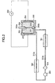
- Fig. 1 and Fig. 2 are schematic views showing a chemical reaction apparatus according to a preferred embodiment of the present invention.
- the chemical reaction apparatus has a reaction vessel 300 having a holding means 206a, 206b for holding a substrate (for example, a silicon wafer or a substrate with a silicon layer) 200, for housing a reaction solution (for example, a liquid containing hydrofluoric acid) 201 and for performing a chemical reaction with the substrate 200 therein; a circulation line 210a (outward path), 210b (inward path) for circulating the reaction solution 201 outside the reaction vessel 300; a deaerating device 301 provided on the circulation line 210a, for removing a gas from the reaction solution 201; and a transfer pump 303 which is a transfer means for transferring the reaction solution 201 on the circulation line 210a.
- the concentration of the gas dissolved in the reaction solution is always maintained at or below the solubility thereof by use of the deaerating device.
- This example is the chemical reaction apparatus for anodization, in which one surface of the substrate 200 is in contact with the reaction solution (for example, a liquid containing hydrofluoric acid) 201 and in which the other surface of the substrate 200 is in contact with an electrolyte 202, which is an electrically conductive solution, and the apparatus is provided with a negative electrode 203 for applying a negative voltage to the reaction solution 201 and a positive electrode 204 for applying a positive voltage to the conductive solution 202.
- the reaction solution for example, a liquid containing hydrofluoric acid
- the substrate 200 is held vertically by the holding means 206a, 206b and this substrate 200 itself separates the reaction solution 201 and the electrolyte 202.
- sealing with seal 205 for example, of Goatex is provided between the holding means and the substrate 200.
- a cooler and/or a heater, or a heat exchanger 302 is provided on the circulation line 210b as occasion may demand, and the reaction solution under circulation is heated or cooled thereby.
- This heating/cooling is preferably carried out so that the temperature of the reaction solution 201 in the reaction vessel 300 is kept within the variation of ⁇ 0.5°C.
- the apparatus is provided with a sensor (not shown) for detecting the temperature of the reaction solution 201 in the reaction vessel 300 and is so arranged as to adjust heating/cooling amounts by the cooler and/or heater, or heat exchanger 302, based on a signal from the sensor.
- Numeral 304 designates a filter, which removes particles of 0.1 ⁇ m or more.
- the deaerating device 301 used in the present invention will be described below.
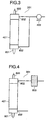
- the deaerating device 301 is composed of a deaerating module 401 and a vacuum pump 400; in the example shown in Fig. 4, the deaerating device 301 is composed of a deaerating module 401 and a water generator 500.
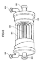
- FIG. 8 A structural example of the deaerating module is shown in Fig. 8.
- the deaerating module 401 has the structure in which hollow-fiber separation membrane sheet 804 woven like a bamboo blind is wound in a spiral form around a perforated water supply pipe 803 having many holes and located in the center, for example, as shown in Fig. 8.
- a perforated water supply pipe 803 having many holes and located in the center, for example, as shown in Fig. 8.
- the hollow fiber separation membrane sheet 804 is made of, for example, a fluororesin such as PFA, and therefore does not suffer deterioration at all even if the reaction solution 200 is a hydrofluoric-acid-based reaction solution, i.e., a liquid containing hydrofluoric acid.
- the inside of the hollow fibers is kept in a pressure reduced state by evacuating the inside by the vacuum pump 400 through hollow fiber ports 802.
- the gas dissolved in the reaction solution 200 efficiently moves from the outside to the inside of the hollow fibers while the reaction solution 200 passes through the laminated portion of the bamboo blind like member of the hollow fibers, and is discharged to the outside of the system through the vacuum pump 400.
- the deaerating device 301 is of the structure of Fig. 4, ultrapure water containing no gas molecule at all, generated by the water generator 500, is forced to the hollow fiber port 802 to be discharged from the other hollow fiber port, whereby a state is kept in which the inside of the hollow fibers is filled with the ultrapure water containing no gas molecule at all.
- the gas molecules in the solution efficiently move from the outside to the inside of the hollow fibers during the period of passage through the laminated portion of the bamboo blind like member of the hollow fibers and are discharged to the outside of the system.
- anodization As the treatments utilizing chemical reactions in the present invention, there may be included such treatments as anodization, anodic oxidation, electrolytic etching, or the like. Among such treatments, examples of anodization will be described.
- the substrate is a substrate 200 comprising p-type single-crystal silicon. It is not impossible to employ the n-type, but a low-resistance substrate has to be selected in that case.
- the substrate 200 is set in the reaction vessel 300 as shown in Fig. 1.
- the reaction vessel 300 is of a completely closed type in order to avoid contact of the solution 201 or electrolyte 202 with the external air. Namely, one side of the substrate 200 is in contact with the hydrofluoric-acid-based reaction solution 201 and the negative electrode 203 is placed on the side of the reaction solution 201.
- the other side of the substrate 200 is in contact with the electrolyte 202 and the positive electrode 204 is placed on the side of the electrolyte 202.
- the electrolyte 202 may be any electrically conductive solution and thus may be the hydrofluoric-acid-based reaction solution. In either case the pore forming reaction takes place from the negative electrode side of the substrate 200 in contact with the hydrofluoric-acid-based solution.
- As the hydrofluoric-acid-based reaction solution 201 concentrated hydrofluoric acid (49 wt% HF) is normally used.
- a surfactant needs to be added into the electrolyte as the reaction solution.
- an alcohol is desired which has the action of lowering the surface tension of the reaction solution 201 and poses no problem of adherence of the surfactant to the substrate 200 in a cleaning step after the anodization.
- an alcohol there may be used, for example, methanol, ethanol, propanol, IPA (isopropyl alcohol), and so on. Since the above example is of the anodization of Si, the reaction solution is the liquid containing hydrofluoric acid; however, it is a matter of course that the reaction solution can be any other non-hydrofluoric-acid-based electrolyte.
- the negative electrode 203 or the positive electrode 204 there may be used a material that is not corroded by the hydrofluoric acid solution, for example, gold (Au), platinum (Pt), or the like.
- the reaction solution 201 in the reaction vessel 300 is circulated through the deaerating device 301 and the cooler/heater 302 as shown in Fig. 2.
- the deaerating device 301 has the structure in which deaerating modules 401 using a gas-permeable membrane are connected in parallel.
- the gas-permeable membrane there exist porous and non-porous ones. Since the circulated solution is the reaction solution containing alcohol serving as a surfactant, the gas-permeable membrane is desirably selected from the non-porous membranes, taking exudation of the reaction solution through the gas-permeable membrane into consideration.
- the deaerating modules 401 have the structure in which the hollow fiber separation membrane sheet woven like the bamboo blind is wound in the spiral form around the perforated supply pipe at the center, and the inside of the hollow fibers is kept in the pressure reduced state by the vacuum pump 400 as shown in Fig. 3.
- the inside of the hollow fibers is kept in the pressure reduced state by the vacuum pump 400, and the gas molecules in the solution efficiently move from the outside to the inside of the hollow fibers during the period of passage through the laminated portions of the hollow fiber bamboo blind like member because of the pressure difference between the inside and outside of the hollow fibers constituted of the gas-permeable membrane, to be discharged through the vacuum pump 400 to the outside of the system.
- the cooler/heater 302 capable of cooling or heating the solution controls the fluctuation of temperature of the reaction solution 201 in the reaction vessel 300 within ⁇ 0.5°C.
- the above arrangement makes it possible to always control the concentration of gas molecules dissolved in the solution at or below the solubility in the chemical reaction in the solution, the gas molecules of by-product are prevented from forming bubbles in the pore forming reaction of silicon and from in turn adhering onto silicon, more specifically to the bottoms of the pores of the silicon, whereby it becomes possible to suppress degradation of chemical reaction rate and nonuniformity of chemical reaction.
- a method for forming porous silicon or a porous silicon substrate by anodizing a single-crystal silicon substrate As the substrate, is provided a substrate 200 comprising p-type single-crystal silicon. It is not impossible to employ the n-type, but a low-resistance substrate has to be selected in that case.
- the substrate 200 is set in the reaction vessel 300 as shown in Fig. 1.
- the reaction vessel 300 is of the completely closed type in order to avoid contact of the solution 201 or electrolyte 202 with the external air. Namely, one side of the substrate 200 is in contact with the hydrofluoric-acid-based reaction solution 201 and the negative electrode 203 is placed on the side of the reaction solution 201. On the other hand, the other side of the substrate 200 is in contact with the electrolyte 202 and the positive electrode 204 is placed on the side of the electrolyte 202.
- the electrolyte 202 may be any electrically conductive solution and thus may be the hydrofluoric-acid-based reaction solution.
- the pore forming reaction occurs from the negative electrode side of the substrate 200 in contact with the hydrofluoric-acid-based solution.
- hydrofluoric-acid-based reaction solution 201 concentrated hydrofluoric acid (49 wt% HF) is normally used.
- the surfactant an alcohol which has the action of lowering the surface tension of the reaction solution 201 and poses no problem of adherence of the surfactant to the substrate 200 in the cleaning step after the anodization.
- the alcohol there may be used, for example, methanol, ethanol, propanol, IPA, and so on.
- the negative electrode 203 or the positive electrode 204 there may be used a material that is not corroded by the hydrofluoric acid solution, for example, gold (Au), platinum (Pt), or the like.
- the reaction solution 201 in the reaction vessel 300 is circulated through the deaerating device 301 and the cooler/heater 302 as shown in Fig. 2.
- the deaerating device 301 has the structure in which deaerating modules 401 using the gas-permeable membrane are connected in parallel.
- As the gas-permeable membrane there exist porous and non-porous ones. Since the circulated solution is the reaction solution containing alcohol serving as a surfactant, the gas-permeable membrane is desirably selected from the non-porous membranes, taking exudation of the reaction solution through the gas-permeable membrane into consideration.
- the deaerating modules 401 have the structure in which the hollow fiber separation membrane sheet woven like the bamboo blind is wound in the spiral form around the perforated supply pipe at the center, and the inside of the hollow fibers is kept in the state filled with the ultrapure water containing no gas molecule at all from the water generator 500 as shown in Fig. 4.
- the inside of the hollow fibers is kept in the state filled with the ultrapure water containing no gas molecule at all, and the gas molecules in the solution efficiently move from the outside to the inside of the hollow fibers during the period of passage through the laminated portions of the hollow fiber bamboo blind like member because of the difference between the internal and external partial pressures of the gas component with respect to the hollow fibers constituted of the gas-permeable membrane, to be discharged to the outside of the system.
- the cooler/heater 302 controls the fluctuation of temperature of the reaction solution 201 in the reaction vessel 300 within ⁇ 0.5°C.
- the above arrangement makes it possible to always control the concentration of gas molecules dissolved in the solution at or below the solubility in the chemical reaction in the solution, the gas molecules of by-product are prevented from forming bubbles in the pore forming reaction of a silicon wafer and from in turn adhering onto the silicon wafer, more specifically, to the bottoms of the pores of the silicon wafer, whereby it becomes possible to suppress degradation of chemical reaction rate and nonuniformity of chemical reaction.
- First prepared was the (100) single-crystal silicon substrate 200 of 152.4 mm (6-inch) p + -substrate having the thickness of 625 ⁇ m, at least the surface layer of which was doped with boron in 1 to 10 ⁇ 10 18 cm -3 , and the surface thereof was subjected to the anodization treatment using a p + -layer of Si as an opposed electrode in a solution of HF/H 2 O/IPA (20 to 30 wt% HF, 10 to 30 wt% IPA). The current density at that time was 5 mA/cm 2 . As shown in Fig. 2, the reaction solution 201 in the reaction vessel 300 was circulated through the deaerating device 301 and the cooler/heater 302.
- the deaerating device 301 was composed of seven deaerating modules 401 formed by use of the non-porous gas-permeable membrane, connected in parallel.
- the deaerating device 301 was kept in the pressure reduced state of about 1.3kPa (10 Torr), using the vacuum pump 400.
- the transfer pump 303 was the one capable of circulating the reaction solution at the flow rate of 70 l/min through the chemical circulation line, i.e., capable of circulating the reaction solution at the flow rate per deaerating module of 10 l/min.
- Amounts of dissolved hydrogen in the reaction solution 201 in the reaction vessel 300 were observed on that occasion, and the result was that during the anodization treatment the amounts of dissolved hydrogen were always approximately 100 ppb or less, far smaller than 1 ppm being the solubility thereof.
- the variation of temperature of the reaction solution 201 in the reaction vessel 300 was always controlled within ⁇ 0.5°C by actuating the cooler/heater 302.
- the anodization treatment was carried out for one minute and the entire surface of the 152.4 mm (6-inch) wafer was observed with a field emission type scanning electron microscope. It was found from the observation that a layer of porous Si having the diameter of pore of 10 nm, the aperture rate of 30%, and the film thickness of 20 ⁇ m was formed with the in-plane uniformity being within the fluctuation of ⁇ 3%. Cross sections of the porous layer were also observed with a transmission electron microscope, with the result that it was confirmed that new crystal defects were not introduced into the porous layer and good single crystallinity was maintained.
- First prepared was the (100) single-crystal silicon substrate 200 of 152.4 mm (6-inch) p + -substrate having the thickness of 625 ⁇ m, at least the surface layer of which was doped with boron in 1 to 10 ⁇ 10 18 cm -3 , and the surface thereof was subjected to the anodization treatment using the p + -layer of Si as an opposed electrode in the solution of HF/H 2 O/IPA (20 to 30 wt% HF, 10 to 30 wt% IPA). The current density at that time was 5 mA/cm 2 . As shown in Fig. 2, the reaction solution 201 in the reaction vessel 300 was circulated through the deaerating device 301 and the cooler/heater 302.
- the deaerating device 301 was composed of seven deaerating modules 401 formed by use of the non-porous gas-permeable membrane, connected in parallel. The deaerating device 301 was kept in the state filled with the ultrapure water containing no gas molecule at all, supplied from the water generator 500.
- the transfer pump 303 was the one capable of circulating the reaction solution at the flow rate of 70 l/min through the chemical circulation line, i.e., capable of circulating the reaction solution at the flow rate per deaerating module of 10 l/min. Amounts of dissolved hydrogen in the reaction solution 201 in the reaction vessel 300 were observed on that occasion, and the result was that during the anodization treatment the amounts of dissolved hydrogen were always approximately 100 ppb or less, far smaller than 1 ppm being the solubility thereof. During the anodization treatment the variation of temperature of the reaction solution 201 in the reaction vessel 300 was always controlled within ⁇ 0.5°C by actuating the cooler/heater 302.
- the anodization treatment was carried out for one minute and the entire surface of the 152.4 mm (6-inch) wafer was observed with the field emission type scanning electron microscope. It was found from the observation that a layer of porous Si having the diameter of pore of 10 nm, the aperture rate of 30%, and the film thickness of 20 ⁇ m was formed with the in-plane uniformity being within the fluctuation of ⁇ 3%.
- First prepared was the (100) single-crystal silicon substrate 200 of 152.4 mm (6-inch) p + -substrate having the thickness of 625 ⁇ m, at least the surface layer of which was doped with boron in 1 to 10 x 10 18 cm -3 , and the surface thereof was subjected to the anodization treatment using the p + -layer of Si as an opposed electrode in the solution of HF/H 2 O/IPA (20 to 30 wt% HF, 10 to 30 wt% IPA). The current density at that time was 5 mA/cm 2 . As shown in Fig. 2, the reaction solution 201 in the reaction vessel 300 was circulated through the deaerating device 301 and the cooler/heater 302.
- the deaerating device 301 was composed of seven deaerating modules 401 formed by use of the non-porous gas-permeable membrane, connected in parallel.
- the deaerating device 301 was kept in the state filled with the ultrapure water containing no gas molecule at all, supplied from the water generator 500.
- the temperature variation of the reaction solution 201 in the reaction vessel 300 was always controlled within ⁇ 0.5 °C by actuating the cooler/heater 302.
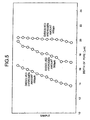
- Fig. 5 shows the dispersion in the depths of pores of the wafer in the respective amounts of dissolved hydrogen. As the amounts of dissolved hydrogen increase, the depths of pores become smaller and the dispersion in the depths of pores increases.
- the porous layer having the diameter of pore of 10 nm and the aperture rate of 30% was formed in the film thickness of 20 ⁇ m and with the in-plane uniformity of film thickness being within the dispersion of ⁇ 3% in the treatment time of one minute.
- First prepared was the (100) single-crystal silicon substrate 200 of 152.4 mm (6-inch) p + -substrate having the thickness of 625 ⁇ m, at least the surface layer of which was doped with boron in 1 to 10 x 10 18 cm -3 , and the surface thereof was subjected to the anodization treatment using the p + -layer of Si as an opposed electrode in the solution of HF/H 2 O/IPA (20 to 30 wt% HF, 10 to 30 wt% IPA). As shown in Fig. 2, the reaction solution 201 in the reaction vessel 300 was circulated through the deaerating device 301 and the cooler/heater 302.
- the deaerating device 301 was composed of seven deaerating modules 401 formed by use of the non-porous gas-permeable membrane, connected in parallel. The deaerating device 301 was kept in the state filled with the ultrapure water containing no gas molecule at all, supplied from the water generator 500.
- the transfer pump 303 was the one capable of circulating the reaction solution at the flow rate of 35 l/min through the chemical circulation line, i.e., capable of circulating the reaction solution at the flow rate per deaerating module of 5 l/min. Amounts of dissolved hydrogen in the reaction solution 201 in the reaction vessel 300 were observed on that occasion, and the result was that during the anodization treatment the amounts of dissolved hydrogen were always approximately 600 ppb during the anodization treatment. During the anodization treatment the variation of temperature of the reaction solution 201 in the reaction vessel 300 was always controlled within ⁇ 0.5 °C by actuating the cooler/heater 302.
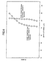
- the anodization treatment was carried out under conditions of different current densities ranging from 5 to 30 mA/cm 2 , and the entire surface of the 152.4 mm (6-inch) wafer was observed thereafter with the field emission type scanning electron microscope.
- Fig. 6 shows the dispersion in the depths of pores of the wafer in the respective current densities.
- the diameters of the pores increase with increase in the current density. It was found that when the amount of dissolved hydrogen in the reaction solution 201 in the reaction vessel 300 was 600 ppb, the fluctuation of in-plane uniformity of film thickness was restrained within ⁇ 3% in formation of the porous layer having the diameter of pore of 20 nm and the depth of pore of 20 ⁇ m, i.e., having the aspect ratio of pore of 1000.
- First prepared was the.(100) single-crystal silicon substrate 200 of 152.4 mm (6-inch) p + -substrate having the thickness of 625 ⁇ m, at least the surface layer of which was doped with boron in 1 to 10 x 10 18 cm -3 , and the surface thereof was subjected to the anodization treatment using the p + -layer of Si as an opposed electrode in the solution of HF/H 2 O/IPA (20 to 30 wt% HF, 10 to 30 wt% IPA). The current density at that time was 5 mA/cm 2 . As shown in Fig. 2, the reaction solution 201 in the reaction vessel 300 was circulated through the deaerating device 301 and the cooler/heater 302.
- the deaerating device 301 was composed of seven deaerating modules 401 formed by use of the non-porous gas-permeable membrane, connected in parallel.
- the deaerating device 301 was kept in the state filled with the ultrapure water containing no gas molecule at all, supplied from the water generator 500.
- the transfer pump 303 was the one capable of circulating the reaction solution at the flow rate of 70 l/min through the chemical circulation line, i.e., capable of circulating the reaction solution at the flow rate per deaerating module of 10 l/min.
- Amounts of dissolved hydrogen in the reaction solution 201 in the reaction vessel 300 were observed on that occasion, and the result was that during the anodization treatment the amounts of dissolved hydrogen were always approximately 100 ppb or less, far smaller than 1 ppm being the solubility thereof.
- the variation of temperature of the reaction solution 201 in the reaction vessel 300 was always controlled within ⁇ 0.5 °C by actuating the cooler/heater 302.
- the anodization treatment was carried out under conditions of different anodization treatment times ranging from 1 to 20 minutes, and the entire surface of the 152.4 mm (6-inch) wafer was observed thereafter with the field emission type scanning electron microscope.
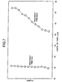
- Fig. 7 shows the dispersion in the depths of pores of the wafer in the respective treatment times.
- the depths of the pores increase with increase in the treatment time. It was found that when the amount of dissolved hydrogen in the reaction solution 201 in the reaction vessel 300 was not more than 100 ppb, the porous layer having the diameter of pore of 10 nm and the aperture rate of 30% was formed in the thickness of 20 ⁇ m and with the in-plane uniformity of thickness being within the dispersion of ⁇ 3% in the treatment time of one minute.
- the present invention achieved efficient removal of gas molecules of by-product in the chemical reactions in a solution, which no conventional technologies have achieved.
- the present invention permits the chemical reactions in a solution to be carried out with high efficiency, high rate, and high uniformity.
- the present invention allows production of the semiconductor substrate that can be applied to formation of the SOI structure, and the invention also permits the semiconductor substrate in which a light-emitting element or a gas sensor can be made, to be produced from an inexpensive silicon substrate.
Abstract
Description
- The present invention relates to a treating method and apparatus utilizing a chemical reaction and, more particularly to a treating method and apparatus utilizing a chemical reaction, applicable to production of chemical industrial goods and semiconductor goods such as integrated circuits or electron devices.
- Treating methods utilizing chemical reactions have been and are applied to many chemical industrial goods and also to semiconductor integrated circuits these years, thus adding abundance to human lives.
- Among the chemical reactions, those in a solution are employed in production of many industrial goods because of their peculiar properties different from those of vapor-phase chemical reactions. Among others, electrolysis reaction is the technology for supplying electric energy to an electrolytic cell to cause change in substance at the interface between the electrode and the electrolyte, thereby producing a chemical substance as an objective material. This technology is applied to production of many industrial goods, including smelting of aluminum, copper, or zinc, metal plating, production of hydrogen, oxygen, caustic soda, and chlorine, and so on.
- There are recent proposals on the ELTRAN (Epitaxial Layer TRANsfer by bond & etch back porous Si) SOI substrate as a method for producing a semiconductor substrate by use of a chemical reaction in a solution in the semiconductor processes (Japanese Patent Application Laid-Open Nos. 5-102445; 5-217992; 5-217821; 5-217820; 5-275663; 5-275329; 6-342784; 7-249749; and 7-235651).
- These utilize the chemical reaction in a solution, called anodization, and are methods for producing a semiconductor substrate characterized by epitaxially growing single-crystal silicon on one porous surface of a silicon single-crystal substrate having made porous a part or all of the surface side by the anodization process, bonding a surface of this epitaxial layer to an arbitrary support substrate, and selectively etching the porous portion of the single-crystal silicon substrate, or removing the non-porous portion by polishing and then selectively etching the porous portion, or separating the bonded substrate into the non-porous portion and an SOI substrate at the porous portion.
- Since the porous silicon formed by the anodization reaction has an enormous surface area and the surface thereof is active to adsorption of an organic gas, a variety of gas sensors utilizing the property are under research (M. B-Chohrin and A. Kurex, "Absorbate effects on photoluminescence and electrical conductivity of porous silicon," Appl. Phys. Lett., vol. 64, pp. 481-483, 1994; A. Richter, "Design considerations and performance of adsorptive humidity sensor with capacitive readout," The 7th Int. Conf. Solid-State Sensors and Actuators, pp. 310-313, 1993; R. C. Anderson, R. S. Muller, and C. W. Tobias, "Investigations of porous silicon for vapor sensing," Sensors and Actuators, A21-A23 pp. 835-839, 1990; Akira Motohashi, "Change in electrical characteristics of anodized silicon/single-crystal silicon samples against water vapor," IEICE Transactions (C-II), vol. J77-C-II, pp. 213-220, 1995).
- As described above, the chemical reactions in a solution are widely used in production of industrial goods, for example, in the chemical industries and the semiconductor industries. Incidentally, from the viewpoint of production of industrial goods, increasing the efficiency of chemical reaction is very important in order to raise economical efficiency of material production or resource savings. Particularly in the semiconductor industries, from the viewpoint of pursuit of cost efficiency, there are two more requirements of increase in rates of such a chemical reaction as film formation or etching and in-plane uniformity of chemical reactions on a large-diameter silicon wafer.
- The chemical reaction in a solution, however, involves generation of a reaction by-product, which is a phenomenon of inhibiting increase in efficiency, rate, and uniformity of chemical reactions. That is, presence in the solution of a further reaction by-product formed by the chemical reaction in addition to the objective chemical substance will inhibit progress of the chemical reaction. A typical example is a phenomenon in the electrolysis in an aqueous solution where hydrogen is normally generated at the negative electrode while oxygen is generated at the positive electrode.
- Since these reactions compete with deposition of an objective metal or a discharge reaction of an inorganic and organic chemical species, they are also significant in terms of current efficiency. In addition, since they can also change the kinds of reaction products, they have extremely important effects. For example, in the production of a semiconductor substrate utilizing the anodization, gas molecules as a reaction by-product inhibit increase in the rate and uniformity of the reaction for forming porous silicon.
- In the conventional technology, as described in the examples of Japanese Patent Application Laid-Open No. 5-102445, the gas molecules generated over the solubility thereof in the solution will form bubbles to adhere to a silicon wafer and the like, thereby inhibiting the reaction. Therefore, the process includes a treatment such as adding alcohol as a surfactant or agitating the solution by use of an agitator. Further, as described in the patent gazette of Japanese Patent Publication No. 8-31460, there is also a method of mounting a bubble removing device in a plating apparatus to remove bubbles contained in a plating solution.
- Patent Abstracts of Japan, Volume 13, No. 378 (E-809), 22 August 1989 discloses a plating apparatus including an air bubble removing unit for removing air bubbles contained in the plating solution. The bubble removing unit employs a membrane with fine pores and bubbles pass through the membrane and are vented to atmosphere.
- United States Patent No. 4,891,103 discloses an anodization system in which surfactant may be added to the reaction solution to reduce its surface tension and reduce the occurrence of bubbles adhering to a wafer surface during anodization.
- These treating methods are temporary solutions, but are not essential solutions. For example, in formation of porous silicon in the production of a semiconductor substrate, pores having diameters of about 10 nm and depths of about 20 µm need to be formed with restraining fluctuation within ±5% as to the diameters of pores and within ±10% as to the depths of pores in the silicon wafer plane. In addition, this process of formation of a porous silicon layer has to be carried out in one minute, which is a standard process time in recent volume production of semiconductors. Assuming that the wafer size is 152.4 mm (6 inches), the diameters of pores are 10 nm, the aperture ratio (area of pores/area of wafer) is 0.3, and the etching rate is 20 µm/min, the rate of generation of hydrogen is 788 cc/min. This large amount of hydrogen is generated at bottoms of fine and long pores having the diameters of 10 nm and the depths of 20 µm, i.e., the aspect ratio of pore of 2000. In order to form the porous silicon layer, the reaction solution has to be always supplied to the bottoms of the fine and long pores having the aspect ratio of 2000 while perfectly removing this large amount of hydrogen as the by-product. It is, however, difficult to solve the above problem by such methods as the addition of a surfactant and the use of agitator. Namely, there is no technology achieved yet for producing the industrial goods including the semiconductor substrates, by utilization of a chemical reaction in a solution, with high productivity.
- An object of the present invention is to provide a method and apparatus wherein a chemical reaction is carried out while the concentration of a gas of a reaction by-product dissolved in a reaction solution in a reaction vessel is always maintained to be not more than its solubility during the reaction.
- In the present invention, the chemical reaction in a solution may be an electrochemical reaction with supply of an electrical energy from outside and, of course, may be an anodization reaction as a kind of electrochemical reactions. Namely, the solution may be an electrolyte.
- According to a first aspect of the present invention, there is provided a chemical reaction method, comprising performing a chemical reaction while always controlling the concentration of a gas of a reaction by-product dissolved in a reaction solution in a reaction vessel to be not more than the solubility thereof during the reaction by deaeration of the reaction solution, said deaeration being carried out using a deaeration module comprising a gas-permeable membrane comprised of hollow fibres;
characterised by: - bringing the hollow fibers into a pressure reduced state by a pump or filling the hollow fibers with ultrapure water containing no gas at all.
-
- Further, it is preferable that during the deaeration the concentration of a gas of a reaction by-product be controlled so as to be not more than 1/10 of the solubility. When the concentration of gas is controlled to be not more than 1/10 of the solubility, for example, in the case of a reaction for forming a porous layer in a surface of a substrate by an anodization reaction where the substrate is held in the reaction vessel, at least one surface of the substrate is kept in contact with the reaction solution, the other surface of the substrate is kept in contact with an electrically conductive solution, a negative voltage is applied to the reaction solution, and a positive voltage is applied to the conductive solution, the porous layer with deep pores having the diameter of 10 nm and the depth of 20 µm, thus having the aspect ratio of pore of 2000, can be formed in a treatment time of one minute while restraining the variation in the depths of pores within ±3% in a plane of a 152.4 mm (6-inch) wafer, by maintaining the amount of dissolved hydrogen in the reaction solution at 1/10 of the solubility.
- In addition, as an absolute value, the concentration of gas is particularly preferably controlled so as to be not more than 100 ppb. When the concentration of gas is controlled to be not more than 100 ppb, for example, in the reaction for forming the porous layer in the surface of substrate by the anodization reaction where the substrate is held in the reaction vessel, one surface of the substrate is kept in contact with the reaction solution, the other surface of the substrate is kept in contact with the electrically conductive solution, the negative voltage is applied to the reaction solution, and the positive voltage is applied to the conductive solution, the porous layer with deep pores having the diameter of 10 nm and the depth of 20 µm, thus having the aspect ratio of pore of 2000, can be formed in the treatment time of one minute while restraining the variation in the depths of pores within ±3% in the 152.4 mm (6-inch) wafer plane.
- There are some cases where the same gas as the reaction by-product exists in the reaction solution from the beginning. Such gas should desirably be removed before the reaction. The gas having particularly great effects is the by-product generated in the chemical reaction. This by-product generated in the chemical reaction needs to be removed at the same time as the generation thereof, so that no bubble of the by-product is generated. For that purpose, it is particularly effective to guide the reaction solution to the outside of the reaction system and to perform deaeration outside the system. Accordingly, the deaeration is preferably carried out in a circulation system.
- Chemical reactions accompanied by generation of by-products are, for example, electrochemical reactions, anodization reactions, and so on, and the present invention is particularly effective in these chemical reactions.
- Particularly, in the case of the reaction of forming the porous layer in the surface of the substrate by the anodization reaction where the substrate is held in the reaction vessel, at least one surface of the substrate is kept in contact with the reaction solution with the other surface of the substrate in contact with the conductive solution, the negative voltage is applied to the reaction solution with the positive voltage applied to the conductive solution, the by-product (gas) will remain in the pores. Especially, this tendency is particularly conspicuous where the diameters of the pores are 20 nm or less, where the depths of pores are 20 µm or more, and where the aspect ratios of the pores are 1000 or more. As a result, nonuniformity occurs in formation of the pores. This tendency is further enhanced in the case of treatments in a shorter time.
- However, in the present invention, even when the diameters of the pores are 10 nm, the depths of the pores are 20 µm, and the aspect ratios of the pores are 2000, formation of uniform pores can be realized even in the case of the treatment time of one minute.
- Further, in the present invention, the reaction solution is preferably isolated from the atmosphere. This is for preventing a gas from mixing from the atmosphere into the reaction solution.
- In the present invention, with regard to the deaerating method for the chemical reaction in a solution, the deaeration may be carried out with a deaerating module comprised of a gas-permeable membrane of hollow fibers, either by evacuating the inside of the hollow fibers to a reduced pressure state preferably by means of a vacuum pump or by filling the inside of the hollow fibers with ultrapure water containing no gas molecule at all.
- In the present invention, with regard to the temperature of the solution, control within the fluctuation of ±0.5°C is preferable in terms of enhancement of controllability of the chemical reaction.
- Another object of the present invention is to provide a chemical reaction apparatus comprising:
- a reaction vessel having a holding means for holding in use a substrate, and for housing in use a reaction solution when carrying out a chemical reaction with a substrate therein;
- a circulation line for circulating the reaction solution outside the reaction vessel;
- a deaerating device provided on the circulation line, for removing a gas from the reaction solution; and
- a transferring means for transferring the reaction solution in the circulation line; characterised in that:
- said deaerating device is comprised of a gas-permeable membrane of hollow fibres, and in that means are provided for bringing the hollow fibres into a reduced pressure state or for filling the inside of the hollow fibres with ultrapure water containing no gas at all.
-
- An example of the chemical reaction apparatus is an apparatus for carrying out the anodization treatment. In a structural example thereof, one surface of a substrate is kept in contact with a reaction solution, the other surface of the substrate is kept in contact with an electrically conductive solution, and there are provided an electrode for applying a negative voltage to the reaction solution and an electrode for applying a positive voltage to the conductive solution. According to the present invention, since in the chemical reaction in a solution the concentration of gas molecules dissolved in the solution is always controlled so as to be not more than the solubility, for example, in the pore formation reaction of silicon by anodization, the gas molecules of the by-product are prevented from forming bubbles and then adhering onto silicon, more particularly onto the bottoms of the pores of silicon, which in turn enables to suppress degradation of chemical reaction rate and occurrence of nonuniform chemical reaction.
- According to the present invention, it is possible to perform pore formation in the silicon substrate for use in the field of ordinary semiconductor integrated circuits, with in-plane uniformity and at high speed. Further, according to the present invention, a semiconductor substrate applicable to formation of SOI structure can be produced. In addition, according to the present invention, it is possible to produce a semiconductor substrate in which a light-emitting element or a gas sensor can be formed, on the basis of an inexpensive silicon substrate.
-
- Fig. 1 is a schematic, cross-sectional view of a reaction vessel according to an embodiment of the present invention;
- Fig. 2 is a schematic view of a chemical reaction apparatus according to an embodiment of the present invention;
- Fig. 3 is a schematic, cross-sectional view of a deaerating module used in the present invention;
- Fig. 4 is a schematic, cross-sectional view of another deaerating module used in the present invention;
- Fig. 5 is a graph showing variations in the depths of pores at respective amounts of dissolved hydrogen in Example 3;
- Fig. 6 is a graph showing variations in the depths of pores at respective current densities in Example 4;
- Fig. 7 is a graph showing variations in the depths of pores at respective treatment times in Example 5; and
- Fig. 8 is a view showing a structural example of the deaerating module.
-
- Fig. 1 and Fig. 2 are schematic views showing a chemical reaction apparatus according to a preferred embodiment of the present invention.
- The chemical reaction apparatus has a
reaction vessel 300 having a holding means 206a, 206b for holding a substrate (for example, a silicon wafer or a substrate with a silicon layer) 200, for housing a reaction solution (for example, a liquid containing hydrofluoric acid) 201 and for performing a chemical reaction with thesubstrate 200 therein; acirculation line 210a (outward path), 210b (inward path) for circulating thereaction solution 201 outside thereaction vessel 300; adeaerating device 301 provided on thecirculation line 210a, for removing a gas from thereaction solution 201; and atransfer pump 303 which is a transfer means for transferring thereaction solution 201 on thecirculation line 210a. In the present invention, during a period in which the substrate is treated by a chemical reaction in thereaction vessel 300, the concentration of the gas dissolved in the reaction solution is always maintained at or below the solubility thereof by use of the deaerating device. - This apparatus will be described in further detail.
- This example is the chemical reaction apparatus for anodization, in which one surface of the
substrate 200 is in contact with the reaction solution (for example, a liquid containing hydrofluoric acid) 201 and in which the other surface of thesubstrate 200 is in contact with anelectrolyte 202, which is an electrically conductive solution, and the apparatus is provided with anegative electrode 203 for applying a negative voltage to thereaction solution 201 and apositive electrode 204 for applying a positive voltage to theconductive solution 202. - The
substrate 200 is held vertically by the holding means 206a, 206b and thissubstrate 200 itself separates thereaction solution 201 and theelectrolyte 202. However, for assuring perfect separation, sealing withseal 205, for example, of Goatex is provided between the holding means and thesubstrate 200. - In this example, a cooler and/or a heater, or a
heat exchanger 302 is provided on thecirculation line 210b as occasion may demand, and the reaction solution under circulation is heated or cooled thereby. This heating/cooling is preferably carried out so that the temperature of thereaction solution 201 in thereaction vessel 300 is kept within the variation of ±0.5°C. For that purpose, the apparatus is provided with a sensor (not shown) for detecting the temperature of thereaction solution 201 in thereaction vessel 300 and is so arranged as to adjust heating/cooling amounts by the cooler and/or heater, orheat exchanger 302, based on a signal from the sensor. -
Numeral 304 designates a filter, which removes particles of 0.1 µm or more. - The
deaerating device 301 used in the present invention will be described below. - Examples of the deaerating device are shown in Fig. 3 and Fig. 4.
- In the example shown in Fig. 3, the
deaerating device 301 is composed of adeaerating module 401 and avacuum pump 400; in the example shown in Fig. 4, thedeaerating device 301 is composed of adeaerating module 401 and awater generator 500. - A structural example of the deaerating module is shown in Fig. 8.
- The
deaerating module 401 has the structure in which hollow-fiberseparation membrane sheet 804 woven like a bamboo blind is wound in a spiral form around a perforatedwater supply pipe 803 having many holes and located in the center, for example, as shown in Fig. 8. By forcing thereaction solution 201 to flow from a treatedsolution inlet 800 into the module, thereaction solution 200 radially flows through the laminated portion of the bamboo blind like member of the hollow fibers toward the periphery and goes out through a treatedsolution outlet 801. The hollow fiberseparation membrane sheet 804 is made of, for example, a fluororesin such as PFA, and therefore does not suffer deterioration at all even if thereaction solution 200 is a hydrofluoric-acid-based reaction solution, i.e., a liquid containing hydrofluoric acid. - In the case where the
deaerating device 301 is of the structure of Fig. 3, the inside of the hollow fibers is kept in a pressure reduced state by evacuating the inside by thevacuum pump 400 throughhollow fiber ports 802. On this occasion, the gas dissolved in thereaction solution 200 efficiently moves from the outside to the inside of the hollow fibers while thereaction solution 200 passes through the laminated portion of the bamboo blind like member of the hollow fibers, and is discharged to the outside of the system through thevacuum pump 400. - In the case where the
deaerating device 301 is of the structure of Fig. 4, ultrapure water containing no gas molecule at all, generated by thewater generator 500, is forced to thehollow fiber port 802 to be discharged from the other hollow fiber port, whereby a state is kept in which the inside of the hollow fibers is filled with the ultrapure water containing no gas molecule at all. On this occasion, because of a difference between internal and external partial pressures of the gas component with respect to the hollow fibers made of a gas-permeable membrane, the gas molecules in the solution efficiently move from the outside to the inside of the hollow fibers during the period of passage through the laminated portion of the bamboo blind like member of the hollow fibers and are discharged to the outside of the system. - As the treatments utilizing chemical reactions in the present invention, there may be included such treatments as anodization, anodic oxidation, electrolytic etching, or the like. Among such treatments, examples of anodization will be described.
- First described is a method for forming porous silicon or a porous silicon substrate by anodizing a single-crystal silicon substrate. The substrate is a
substrate 200 comprising p-type single-crystal silicon. It is not impossible to employ the n-type, but a low-resistance substrate has to be selected in that case. Thesubstrate 200 is set in thereaction vessel 300 as shown in Fig. 1. Thereaction vessel 300 is of a completely closed type in order to avoid contact of thesolution 201 orelectrolyte 202 with the external air. Namely, one side of thesubstrate 200 is in contact with the hydrofluoric-acid-basedreaction solution 201 and thenegative electrode 203 is placed on the side of thereaction solution 201. On the other hand, the other side of thesubstrate 200 is in contact with theelectrolyte 202 and thepositive electrode 204 is placed on the side of theelectrolyte 202. Theelectrolyte 202 may be any electrically conductive solution and thus may be the hydrofluoric-acid-based reaction solution. In either case the pore forming reaction takes place from the negative electrode side of thesubstrate 200 in contact with the hydrofluoric-acid-based solution. As the hydrofluoric-acid-basedreaction solution 201, concentrated hydrofluoric acid (49 wt% HF) is normally used. - For the purpose of facilitating invasion of the hydrofluoric-acid-based
reaction solution 201 into the pores of thesubstrate 200 having the diameter of about 10 nm during formation of porous silicon by the anodization reaction, a surfactant needs to be added into the electrolyte as the reaction solution. As the surfactant, an alcohol is desired which has the action of lowering the surface tension of thereaction solution 201 and poses no problem of adherence of the surfactant to thesubstrate 200 in a cleaning step after the anodization. As such an alcohol, there may be used, for example, methanol, ethanol, propanol, IPA (isopropyl alcohol), and so on. Since the above example is of the anodization of Si, the reaction solution is the liquid containing hydrofluoric acid; however, it is a matter of course that the reaction solution can be any other non-hydrofluoric-acid-based electrolyte. - As to the
negative electrode 203 or thepositive electrode 204, there may be used a material that is not corroded by the hydrofluoric acid solution, for example, gold (Au), platinum (Pt), or the like. - The
reaction solution 201 in thereaction vessel 300 is circulated through thedeaerating device 301 and the cooler/heater 302 as shown in Fig. 2. Thedeaerating device 301 has the structure in whichdeaerating modules 401 using a gas-permeable membrane are connected in parallel. - As the gas-permeable membrane, there exist porous and non-porous ones. Since the circulated solution is the reaction solution containing alcohol serving as a surfactant, the gas-permeable membrane is desirably selected from the non-porous membranes, taking exudation of the reaction solution through the gas-permeable membrane into consideration. The deaerating
modules 401 have the structure in which the hollow fiber separation membrane sheet woven like the bamboo blind is wound in the spiral form around the perforated supply pipe at the center, and the inside of the hollow fibers is kept in the pressure reduced state by thevacuum pump 400 as shown in Fig. 3. More specifically, the inside of the hollow fibers is kept in the pressure reduced state by thevacuum pump 400, and the gas molecules in the solution efficiently move from the outside to the inside of the hollow fibers during the period of passage through the laminated portions of the hollow fiber bamboo blind like member because of the pressure difference between the inside and outside of the hollow fibers constituted of the gas-permeable membrane, to be discharged through thevacuum pump 400 to the outside of the system. - The cooler/
heater 302 capable of cooling or heating the solution controls the fluctuation of temperature of thereaction solution 201 in thereaction vessel 300 within ±0.5°C. - Since the above arrangement makes it possible to always control the concentration of gas molecules dissolved in the solution at or below the solubility in the chemical reaction in the solution, the gas molecules of by-product are prevented from forming bubbles in the pore forming reaction of silicon and from in turn adhering onto silicon, more specifically to the bottoms of the pores of the silicon, whereby it becomes possible to suppress degradation of chemical reaction rate and nonuniformity of chemical reaction.
- Next described is a method for forming porous silicon or a porous silicon substrate by anodizing a single-crystal silicon substrate. As the substrate, is provided a
substrate 200 comprising p-type single-crystal silicon. It is not impossible to employ the n-type, but a low-resistance substrate has to be selected in that case. - The
substrate 200 is set in thereaction vessel 300 as shown in Fig. 1. Thereaction vessel 300 is of the completely closed type in order to avoid contact of thesolution 201 orelectrolyte 202 with the external air. Namely, one side of thesubstrate 200 is in contact with the hydrofluoric-acid-basedreaction solution 201 and thenegative electrode 203 is placed on the side of thereaction solution 201. On the other hand, the other side of thesubstrate 200 is in contact with theelectrolyte 202 and thepositive electrode 204 is placed on the side of theelectrolyte 202. Theelectrolyte 202 may be any electrically conductive solution and thus may be the hydrofluoric-acid-based reaction solution. In either case the pore forming reaction occurs from the negative electrode side of thesubstrate 200 in contact with the hydrofluoric-acid-based solution. As the hydrofluoric-acid-basedreaction solution 201, concentrated hydrofluoric acid (49 wt% HF) is normally used. - For the purpose of facilitating invasion of the hydrofluoric-acid-based
reaction solution 201 into the pores of thesubstrate 200 having the diameter of about 10 nm during formation of porous silicon by the anodization reaction, it is desirable to add the surfactant. As the surfactant, an alcohol is desired which has the action of lowering the surface tension of thereaction solution 201 and poses no problem of adherence of the surfactant to thesubstrate 200 in the cleaning step after the anodization. As the alcohol, there may be used, for example, methanol, ethanol, propanol, IPA, and so on. - As to the
negative electrode 203 or thepositive electrode 204, there may be used a material that is not corroded by the hydrofluoric acid solution, for example, gold (Au), platinum (Pt), or the like. - The
reaction solution 201 in thereaction vessel 300 is circulated through thedeaerating device 301 and the cooler/heater 302 as shown in Fig. 2. Thedeaerating device 301 has the structure in whichdeaerating modules 401 using the gas-permeable membrane are connected in parallel. As the gas-permeable membrane, there exist porous and non-porous ones. Since the circulated solution is the reaction solution containing alcohol serving as a surfactant, the gas-permeable membrane is desirably selected from the non-porous membranes, taking exudation of the reaction solution through the gas-permeable membrane into consideration. - The deaerating
modules 401 have the structure in which the hollow fiber separation membrane sheet woven like the bamboo blind is wound in the spiral form around the perforated supply pipe at the center, and the inside of the hollow fibers is kept in the state filled with the ultrapure water containing no gas molecule at all from thewater generator 500 as shown in Fig. 4. More specifically, the inside of the hollow fibers is kept in the state filled with the ultrapure water containing no gas molecule at all, and the gas molecules in the solution efficiently move from the outside to the inside of the hollow fibers during the period of passage through the laminated portions of the hollow fiber bamboo blind like member because of the difference between the internal and external partial pressures of the gas component with respect to the hollow fibers constituted of the gas-permeable membrane, to be discharged to the outside of the system. - The cooler/
heater 302 controls the fluctuation of temperature of thereaction solution 201 in thereaction vessel 300 within ±0.5°C. - Since the above arrangement makes it possible to always control the concentration of gas molecules dissolved in the solution at or below the solubility in the chemical reaction in the solution, the gas molecules of by-product are prevented from forming bubbles in the pore forming reaction of a silicon wafer and from in turn adhering onto the silicon wafer, more specifically, to the bottoms of the pores of the silicon wafer, whereby it becomes possible to suppress degradation of chemical reaction rate and nonuniformity of chemical reaction.
- The present invention will be described in more detail with specific examples thereof, but it should be noted that the present invention is by no means intended to be limited to these examples.
- First prepared was the (100) single-
crystal silicon substrate 200 of 152.4 mm (6-inch) p+-substrate having the thickness of 625 µm, at least the surface layer of which was doped with boron in 1 to 10 × 1018 cm-3, and the surface thereof was subjected to the anodization treatment using a p+-layer of Si as an opposed electrode in a solution of HF/H2O/IPA (20 to 30 wt% HF, 10 to 30 wt% IPA). The current density at that time was 5 mA/cm2. As shown in Fig. 2, thereaction solution 201 in thereaction vessel 300 was circulated through thedeaerating device 301 and the cooler/heater 302. - The
deaerating device 301 was composed of sevendeaerating modules 401 formed by use of the non-porous gas-permeable membrane, connected in parallel. Thedeaerating device 301 was kept in the pressure reduced state of about 1.3kPa (10 Torr), using thevacuum pump 400. Thetransfer pump 303 was the one capable of circulating the reaction solution at the flow rate of 70 l/min through the chemical circulation line, i.e., capable of circulating the reaction solution at the flow rate per deaerating module of 10 l/min. Amounts of dissolved hydrogen in thereaction solution 201 in thereaction vessel 300 were observed on that occasion, and the result was that during the anodization treatment the amounts of dissolved hydrogen were always approximately 100 ppb or less, far smaller than 1 ppm being the solubility thereof. During the anodization treatment the variation of temperature of thereaction solution 201 in thereaction vessel 300 was always controlled within ±0.5°C by actuating the cooler/heater 302. - Under the above conditions, the anodization treatment was carried out for one minute and the entire surface of the 152.4 mm (6-inch) wafer was observed with a field emission type scanning electron microscope. It was found from the observation that a layer of porous Si having the diameter of pore of 10 nm, the aperture rate of 30%, and the film thickness of 20 µm was formed with the in-plane uniformity being within the fluctuation of ±3%. Cross sections of the porous layer were also observed with a transmission electron microscope, with the result that it was confirmed that new crystal defects were not introduced into the porous layer and good single crystallinity was maintained.
- First prepared was the (100) single-
crystal silicon substrate 200 of 152.4 mm (6-inch) p+-substrate having the thickness of 625 µm, at least the surface layer of which was doped with boron in 1 to 10 × 1018 cm-3, and the surface thereof was subjected to the anodization treatment using the p+-layer of Si as an opposed electrode in the solution of HF/H2O/IPA (20 to 30 wt% HF, 10 to 30 wt% IPA). The current density at that time was 5 mA/cm2. As shown in Fig. 2, thereaction solution 201 in thereaction vessel 300 was circulated through thedeaerating device 301 and the cooler/heater 302. Thedeaerating device 301 was composed of sevendeaerating modules 401 formed by use of the non-porous gas-permeable membrane, connected in parallel. Thedeaerating device 301 was kept in the state filled with the ultrapure water containing no gas molecule at all, supplied from thewater generator 500. - The
transfer pump 303 was the one capable of circulating the reaction solution at the flow rate of 70 l/min through the chemical circulation line, i.e., capable of circulating the reaction solution at the flow rate per deaerating module of 10 l/min. Amounts of dissolved hydrogen in thereaction solution 201 in thereaction vessel 300 were observed on that occasion, and the result was that during the anodization treatment the amounts of dissolved hydrogen were always approximately 100 ppb or less, far smaller than 1 ppm being the solubility thereof. During the anodization treatment the variation of temperature of thereaction solution 201 in thereaction vessel 300 was always controlled within ±0.5°C by actuating the cooler/heater 302. - Under the above conditions, the anodization treatment was carried out for one minute and the entire surface of the 152.4 mm (6-inch) wafer was observed with the field emission type scanning electron microscope. It was found from the observation that a layer of porous Si having the diameter of pore of 10 nm, the aperture rate of 30%, and the film thickness of 20 µm was formed with the in-plane uniformity being within the fluctuation of ±3%.
- Cross sections of the porous layer were also observed with the transmission electron microscope, with the result that it was confirmed that new crystal defects were not introduced into the porous layer and good single crystallinity was maintained.
- In this example the influence of deaerating amount of gas was studied.
- First prepared was the (100) single-
crystal silicon substrate 200 of 152.4 mm (6-inch) p+-substrate having the thickness of 625 µm, at least the surface layer of which was doped with boron in 1 to 10 x 1018 cm-3, and the surface thereof was subjected to the anodization treatment using the p+-layer of Si as an opposed electrode in the solution of HF/H2O/IPA (20 to 30 wt% HF, 10 to 30 wt% IPA). The current density at that time was 5 mA/cm2. As shown in Fig. 2, thereaction solution 201 in thereaction vessel 300 was circulated through thedeaerating device 301 and the cooler/heater 302. Thedeaerating device 301 was composed of sevendeaerating modules 401 formed by use of the non-porous gas-permeable membrane, connected in parallel. Thedeaerating device 301 was kept in the state filled with the ultrapure water containing no gas molecule at all, supplied from thewater generator 500. During the anodization treatment the temperature variation of thereaction solution 201 in thereaction vessel 300 was always controlled within ±0.5 °C by actuating the cooler/heater 302. - Under the above conditions the anodization treatment was carried out for one minute at different flow rates of the
transfer pump 301 ranging from 0 to 70 l/min. Amounts of dissolved hydrogen in thereaction solution 201 in thereaction vessel 300 were measured during the anodization treatment under the conditions of the respective flow rates, and after the treatment the entire surface of the 152.4 mm (6-inch) wafer was observed with the field emission type scanning electron microscope. Fig. 5 shows the dispersion in the depths of pores of the wafer in the respective amounts of dissolved hydrogen. As the amounts of dissolved hydrogen increase, the depths of pores become smaller and the dispersion in the depths of pores increases. It was found that when the amount of dissolved hydrogen in thereaction solution 201 in thereaction vessel 300 was not more than 100 ppb, the porous layer having the diameter of pore of 10 nm and the aperture rate of 30% was formed in the film thickness of 20 µm and with the in-plane uniformity of film thickness being within the dispersion of ±3% in the treatment time of one minute. - In this example the influence of diameter of pore was studied.
- First prepared was the (100) single-
crystal silicon substrate 200 of 152.4 mm (6-inch) p+-substrate having the thickness of 625 µm, at least the surface layer of which was doped with boron in 1 to 10 x 1018 cm-3, and the surface thereof was subjected to the anodization treatment using the p+-layer of Si as an opposed electrode in the solution of HF/H2O/IPA (20 to 30 wt% HF, 10 to 30 wt% IPA). As shown in Fig. 2, thereaction solution 201 in thereaction vessel 300 was circulated through thedeaerating device 301 and the cooler/heater 302. Thedeaerating device 301 was composed of sevendeaerating modules 401 formed by use of the non-porous gas-permeable membrane, connected in parallel. Thedeaerating device 301 was kept in the state filled with the ultrapure water containing no gas molecule at all, supplied from thewater generator 500. - The
transfer pump 303 was the one capable of circulating the reaction solution at the flow rate of 35 l/min through the chemical circulation line, i.e., capable of circulating the reaction solution at the flow rate per deaerating module of 5 l/min. Amounts of dissolved hydrogen in thereaction solution 201 in thereaction vessel 300 were observed on that occasion, and the result was that during the anodization treatment the amounts of dissolved hydrogen were always approximately 600 ppb during the anodization treatment. During the anodization treatment the variation of temperature of thereaction solution 201 in thereaction vessel 300 was always controlled within ±0.5 °C by actuating the cooler/heater 302. - Under the above conditions the anodization treatment was carried out under conditions of different current densities ranging from 5 to 30 mA/cm2, and the entire surface of the 152.4 mm (6-inch) wafer was observed thereafter with the field emission type scanning electron microscope.
- Fig. 6 shows the dispersion in the depths of pores of the wafer in the respective current densities. In the anodization reaction the diameters of the pores increase with increase in the current density. It was found that when the amount of dissolved hydrogen in the
reaction solution 201 in thereaction vessel 300 was 600 ppb, the fluctuation of in-plane uniformity of film thickness was restrained within ±3% in formation of the porous layer having the diameter of pore of 20 nm and the depth of pore of 20 µm, i.e., having the aspect ratio of pore of 1000. It was, however, found that the in-plane uniformity of thickness was degraded down to ±10% in the case of relatively deeper pores having the diameter of pore of 10 nm and the depth of pore of 20 µm, i.e., having the aspect ratio of pore of 2000. - In this example the influence of depth of pore was studied.
- First prepared was the.(100) single-
crystal silicon substrate 200 of 152.4 mm (6-inch) p+-substrate having the thickness of 625 µm, at least the surface layer of which was doped with boron in 1 to 10 x 1018 cm-3, and the surface thereof was subjected to the anodization treatment using the p+-layer of Si as an opposed electrode in the solution of HF/H2O/IPA (20 to 30 wt% HF, 10 to 30 wt% IPA). The current density at that time was 5 mA/cm2. As shown in Fig. 2, thereaction solution 201 in thereaction vessel 300 was circulated through thedeaerating device 301 and the cooler/heater 302. Thedeaerating device 301 was composed of sevendeaerating modules 401 formed by use of the non-porous gas-permeable membrane, connected in parallel. Thedeaerating device 301 was kept in the state filled with the ultrapure water containing no gas molecule at all, supplied from thewater generator 500. Thetransfer pump 303 was the one capable of circulating the reaction solution at the flow rate of 70 l/min through the chemical circulation line, i.e., capable of circulating the reaction solution at the flow rate per deaerating module of 10 l/min. Amounts of dissolved hydrogen in thereaction solution 201 in thereaction vessel 300 were observed on that occasion, and the result was that during the anodization treatment the amounts of dissolved hydrogen were always approximately 100 ppb or less, far smaller than 1 ppm being the solubility thereof. During the anodization treatment the variation of temperature of thereaction solution 201 in thereaction vessel 300 was always controlled within ±0.5 °C by actuating the cooler/heater 302. - Under the above conditions the anodization treatment was carried out under conditions of different anodization treatment times ranging from 1 to 20 minutes, and the entire surface of the 152.4 mm (6-inch) wafer was observed thereafter with the field emission type scanning electron microscope.
- Fig. 7 shows the dispersion in the depths of pores of the wafer in the respective treatment times. In the anodization reaction the depths of the pores increase with increase in the treatment time. It was found that when the amount of dissolved hydrogen in the
reaction solution 201 in thereaction vessel 300 was not more than 100 ppb, the porous layer having the diameter of pore of 10 nm and the aperture rate of 30% was formed in the thickness of 20 µm and with the in-plane uniformity of thickness being within the dispersion of ±3% in the treatment time of one minute. It was, however, found that the in-plane uniformity of thickness was degraded down to ±10% in the case of deeper pores having the diameter of pore of 10 nm and the depth of pore of 40 µm, i.e., having the aspect ratio of pore of 4000. - The present invention achieved efficient removal of gas molecules of by-product in the chemical reactions in a solution, which no conventional technologies have achieved. As a result, the present invention permits the chemical reactions in a solution to be carried out with high efficiency, high rate, and high uniformity. Further, the present invention allows production of the semiconductor substrate that can be applied to formation of the SOI structure, and the invention also permits the semiconductor substrate in which a light-emitting element or a gas sensor can be made, to be produced from an inexpensive silicon substrate.
Claims (26)
- A chemical reaction method, comprising performing a chemical reaction while always controlling the concentration of a gas of a reaction by-product dissolved in a reaction solution (201) in a reaction vessel (300) to be not more than the solubility thereof during the reaction by deaeration of the reaction solution (201), said deaeration being carried out using a deaeration module comprising a gas-permeable membrane comprised of hollow fibres;
characterised by:bringing the hollow fibers into a pressure reduced state by a pump or filling the hollow fibers with ultrapure water containing no gas at all. - A method according to claim 1, wherein the reaction solution (201) is circulated outside the reaction vessel (300), and wherein deaeration of the reaction solution (201) is carried out on the way of circulation.
- A method according to claim 1, wherein the concentration of the gas is controlled to be not more than 1/10 of the solubility.
- A method according to claim 1, wherein the concentration of the gas is controlled to be not more than 100 ppb.
- A method according to claim 1, wherein the reaction by-product is hydrogen.
- A method according to claim 1, wherein the chemical reaction is an electrochemical reaction.
- A method according to claim 1, wherein the chemical reaction is an anodization reaction.
- A method according to claim 7, wherein the anodization reaction is a reaction for forming a porous layer in a surface of a substrate (200).
- A method according to claim 8, wherein the substrate (200) is held in the reaction vessel (300), one surface of the substrate (200) is kept in contact with the reaction solution (201), the other surface of the substrate is kept in contact with an electrically conductive solution (202), a negative voltage is applied to the reaction solution, and a positive voltage is applied to the conductive solution.
- A method-according to claim 1, wherein the reaction solution (201) in the reaction vessel is isolated from the atmosphere.
- A method according to claim 10, wherein the reaction solution (201) is a liquid containing hydrofluoric acid.
- A method according to claim 8, wherein a surfactant is added into the reaction solution (201).
- A method according to claim 12, wherein the surfactant is selected from the group consisting of methanol, ethanol and isopropyl alcohol.
- A method according to claim 8, wherein the diameters of the pores are not more than 20 nm.
- A method according to claim 8, wherein the depths of the pores are not less than 20 µm.
- A method according to claim 8, wherein the aspect ratios of the pores are not less than 1000.
- A method according to claim 8, wherein the substrate (200) is a silicon wafer.
- A method according to claim 1, wherein fluctuation of the temperature of the reaction solution is controlled within ±0.5°C.
- A chemical reaction apparatus comprising:characterised in that:a reaction vessel (300) having a holding means (206a,206b) for holding in use a substrate (200), and for housing in use a reaction solution (201) when carrying out a chemical reaction with a substrate (200) therein;a circulation line (201a,201b) for circulating the reaction solution (201) outside the reaction vessel (300);a deaerating device (301) provided on the circulation line, for removing a gas from the reaction solution; anda transferring means (303) for transferring the reaction solution in the circulation line;said deaerating device is comprised of a gas-permeable membrane (804) of hollow fibres, and in that means (400,500) are provided for bringing the hollow fibres into a reduced pressure state or for filling the inside of the hollow fibres with ultrapure water containing no gas at all.
- Apparatus according to claim 19, wherein, in use, one surface of the substrate (200) is kept in contact with the reaction solution (201) and the other surface of the substrate is kept in contact with an electrically conductive solution (202), further comprising an electrode (203) for applying a negative voltage to the reaction solution and an electrode (204) for applying a positive voltage to the electrically conductive solution.
- Apparatus according to claim 19, wherein the reaction vessel (300) is of a hermetically closed type.
- Apparatus according to claim 19, wherein the reaction solution (201) is a liquid containing hydrofluoric acid.
- Apparatus according to claim 19, wherein the means for bringing the hollow fibers into a pressure reduced state is a pump.
- Apparatus according to claim 19, wherein the means (500) for filling the inside of the hollow fibers with ultrapure water containing no gas at all is a water generator.
- Apparatus according to claim 19, wherein means (302) for controlling fluctuation of the temperature of the reaction solution within ±0.5°C is provided on the circulation line.
- A treating method, comprising performing a chemical reaction according to any one of claims 1 to 18 to treat a body to be treated while always maintaining the concentration of a gas of a reaction by-product dissolved in a reaction solution in contact with the body to be treated in a reaction vessel to be not more than the solubility thereof during the reaction.
Applications Claiming Priority (3)
| Application Number | Priority Date | Filing Date | Title |
|---|---|---|---|
| JP123783/97 | 1997-05-14 | ||
| JP12378397 | 1997-05-14 | ||
| JP12378397A JP3985065B2 (en) | 1997-05-14 | 1997-05-14 | Porous silicon substrate forming method and porous silicon substrate forming apparatus |
Publications (3)
| Publication Number | Publication Date |
|---|---|
| EP0879902A2 EP0879902A2 (en) | 1998-11-25 |
| EP0879902A3 EP0879902A3 (en) | 1999-12-29 |
| EP0879902B1 true EP0879902B1 (en) | 2003-08-13 |
Family
ID=14869193
Family Applications (1)
| Application Number | Title | Priority Date | Filing Date |
|---|---|---|---|
| EP98303765A Expired - Lifetime EP0879902B1 (en) | 1997-05-14 | 1998-05-13 | Treating method and apparatus utilizing chemical reaction |
Country Status (6)
| Country | Link |
|---|---|
| US (1) | US6258244B1 (en) |
| EP (1) | EP0879902B1 (en) |
| JP (1) | JP3985065B2 (en) |
| KR (1) | KR100306839B1 (en) |
| DE (1) | DE69817077T2 (en) |
| TW (1) | TW463219B (en) |
Cited By (2)
| Publication number | Priority date | Publication date | Assignee | Title |
|---|---|---|---|---|
| US8926803B2 (en) | 2009-01-15 | 2015-01-06 | Solexel, Inc. | Porous silicon electro-etching system and method |
| US10829864B2 (en) | 2009-01-15 | 2020-11-10 | Trutag Technologies, Inc. | Apparatus and methods for uniformly forming porous semiconductor on a substrate |
Families Citing this family (24)
| Publication number | Priority date | Publication date | Assignee | Title |
|---|---|---|---|---|
| TW522455B (en) * | 1998-11-09 | 2003-03-01 | Ebara Corp | Plating method and apparatus therefor |
| US7022211B2 (en) * | 2000-01-31 | 2006-04-04 | Ebara Corporation | Semiconductor wafer holder and electroplating system for plating a semiconductor wafer |
| JP3979847B2 (en) * | 2000-03-17 | 2007-09-19 | 株式会社荏原製作所 | Plating equipment |
| JP2002363792A (en) * | 2001-06-01 | 2002-12-18 | Tokyo Electron Ltd | Liquid treatment system and liquid treatment method |
| JP4821067B2 (en) * | 2001-08-01 | 2011-11-24 | ソニー株式会社 | Anodizing apparatus, method for forming porous layer using the same, and method for producing semiconductor thin film |
| JP2003129283A (en) * | 2001-10-18 | 2003-05-08 | Hitachi Ltd | Plating device and process for manufacturing semiconductor device using the same |
| KR101148332B1 (en) | 2003-04-30 | 2012-05-25 | 크리, 인코포레이티드 | High powered light emitter packages with compact optics |
| US7005679B2 (en) | 2003-05-01 | 2006-02-28 | Cree, Inc. | Multiple component solid state white light |
| US6972438B2 (en) * | 2003-09-30 | 2005-12-06 | Cree, Inc. | Light emitting diode with porous SiC substrate and method for fabricating |
| EP1969633B1 (en) | 2005-12-22 | 2018-08-29 | Cree, Inc. | Lighting device |
| EP2011164B1 (en) | 2006-04-24 | 2018-08-29 | Cree, Inc. | Side-view surface mount white led |
| US7834367B2 (en) | 2007-01-19 | 2010-11-16 | Cree, Inc. | Low voltage diode with reduced parasitic resistance and method for fabricating |
| US9012937B2 (en) | 2007-10-10 | 2015-04-21 | Cree, Inc. | Multiple conversion material light emitting diode package and method of fabricating same |
| US9431589B2 (en) | 2007-12-14 | 2016-08-30 | Cree, Inc. | Textured encapsulant surface in LED packages |
| US8999058B2 (en) * | 2009-05-05 | 2015-04-07 | Solexel, Inc. | High-productivity porous semiconductor manufacturing equipment |
| US9076642B2 (en) | 2009-01-15 | 2015-07-07 | Solexel, Inc. | High-Throughput batch porous silicon manufacturing equipment design and processing methods |
| CN102844883B (en) | 2010-02-12 | 2016-01-20 | 速力斯公司 | For the manufacture of the two-sided reusable template of the Semiconductor substrate of photocell and microelectronic component |
| US8992746B2 (en) | 2010-12-02 | 2015-03-31 | Dainippon Screen Mfg. Co., Ltd. | Anodizing apparatus |
| JP6037779B2 (en) * | 2012-11-01 | 2016-12-07 | 株式会社ダルトン | Anodizing apparatus, anodizing system and anodizing method |
| JP6045309B2 (en) * | 2012-11-09 | 2016-12-14 | 株式会社ダルトン | Anodizing apparatus, anodizing system and anodizing method |
| CN104241262B (en) | 2013-06-14 | 2020-11-06 | 惠州科锐半导体照明有限公司 | Light emitting device and display device |
| CN103276436A (en) * | 2013-06-17 | 2013-09-04 | 天津大学 | Preparation method of novel ordered nano-porous silicon |
| CN103395740A (en) * | 2013-08-02 | 2013-11-20 | 合肥工业大学 | Method for selectively preparing porous silicon based on silicon on insulator |
| US9799541B1 (en) * | 2014-12-18 | 2017-10-24 | Trutag Technologies, Inc. | Multiple wafer single bath etcher |
Family Cites Families (17)
| Publication number | Priority date | Publication date | Assignee | Title |
|---|---|---|---|---|
| FR2615036B1 (en) | 1987-05-05 | 1989-08-18 | France Etat | MACHINE FOR THE MANUFACTURE OF POROUS SILICON |
| JPH0831460B2 (en) * | 1987-11-13 | 1996-03-27 | 富士通株式会社 | Plating equipment |
| US4891103A (en) | 1988-08-23 | 1990-01-02 | Texas Instruments Incorporated | Anadization system with remote voltage sensing and active feedback control capabilities |
| US5443727A (en) * | 1990-10-30 | 1995-08-22 | Minnesota Mining And Manufacturing Company | Articles having a polymeric shell and method for preparing same |
| JP3347354B2 (en) | 1991-02-15 | 2002-11-20 | キヤノン株式会社 | Etching method and method of manufacturing semiconductor substrate |
| JP3112106B2 (en) | 1991-10-11 | 2000-11-27 | キヤノン株式会社 | Manufacturing method of semiconductor substrate |
| JP2994837B2 (en) | 1992-01-31 | 1999-12-27 | キヤノン株式会社 | Semiconductor substrate flattening method, semiconductor substrate manufacturing method, and semiconductor substrate |
| JP3171903B2 (en) | 1992-01-30 | 2001-06-04 | キヤノン株式会社 | Semiconductor substrate and manufacturing method thereof |
| JP3250673B2 (en) | 1992-01-31 | 2002-01-28 | キヤノン株式会社 | Semiconductor element substrate and method of manufacturing the same |
| JP3416163B2 (en) | 1992-01-31 | 2003-06-16 | キヤノン株式会社 | Semiconductor substrate and manufacturing method thereof |
| JP3261685B2 (en) | 1992-01-31 | 2002-03-04 | キヤノン株式会社 | Semiconductor element substrate and method of manufacturing the same |
| DE69312636T2 (en) * | 1992-11-09 | 1998-02-05 | Canon Kk | Anodizing apparatus with a carrier device for the substrate to be treated |
| US5338416A (en) * | 1993-02-05 | 1994-08-16 | Massachusetts Institute Of Technology | Electrochemical etching process |
| JP3262470B2 (en) | 1993-12-28 | 2002-03-04 | キヤノン株式会社 | Semiconductor substrate and manufacturing method thereof |
| JP3294934B2 (en) | 1994-03-11 | 2002-06-24 | キヤノン株式会社 | Method for manufacturing semiconductor substrate and semiconductor substrate |
| US5464509A (en) * | 1994-05-20 | 1995-11-07 | Massachusetts Institute Of Technology | P-N junction etch-stop technique for electrochemical etching of semiconductors |
| JP2979963B2 (en) | 1994-07-21 | 1999-11-22 | 日本電池株式会社 | Rechargeable battery |
-
1997
- 1997-05-14 JP JP12378397A patent/JP3985065B2/en not_active Expired - Fee Related
-
1998
- 1998-05-13 EP EP98303765A patent/EP0879902B1/en not_active Expired - Lifetime
- 1998-05-13 DE DE69817077T patent/DE69817077T2/en not_active Expired - Lifetime
- 1998-05-13 US US09/076,834 patent/US6258244B1/en not_active Expired - Lifetime
- 1998-05-14 TW TW087107467A patent/TW463219B/en active
- 1998-05-14 KR KR1019980017312A patent/KR100306839B1/en not_active IP Right Cessation
Cited By (2)
| Publication number | Priority date | Publication date | Assignee | Title |
|---|---|---|---|---|
| US8926803B2 (en) | 2009-01-15 | 2015-01-06 | Solexel, Inc. | Porous silicon electro-etching system and method |
| US10829864B2 (en) | 2009-01-15 | 2020-11-10 | Trutag Technologies, Inc. | Apparatus and methods for uniformly forming porous semiconductor on a substrate |
Also Published As
| Publication number | Publication date |
|---|---|
| TW463219B (en) | 2001-11-11 |
| US6258244B1 (en) | 2001-07-10 |
| EP0879902A2 (en) | 1998-11-25 |
| EP0879902A3 (en) | 1999-12-29 |
| DE69817077T2 (en) | 2004-06-03 |
| KR100306839B1 (en) | 2001-10-19 |
| DE69817077D1 (en) | 2003-09-18 |
| JP3985065B2 (en) | 2007-10-03 |
| KR19980087032A (en) | 1998-12-05 |
| JPH10312990A (en) | 1998-11-24 |
Similar Documents
| Publication | Publication Date | Title |
|---|---|---|
| EP0879902B1 (en) | Treating method and apparatus utilizing chemical reaction | |
| KR100287502B1 (en) | Semiconductor processing system and substrate processing system | |
| KR100385255B1 (en) | Method of cleaning porous body, and process for producing porous body, non-porous film or bonded substrate | |
| US5635053A (en) | Method and apparatus for cleaning electronic parts | |
| US6547938B1 (en) | Anodizing apparatus, utilizing a perforated negative electrode | |
| US20030008473A1 (en) | Anodizing method and apparatus and semiconductor substrate manufacturing method | |
| KR100504413B1 (en) | Apparatus and method for etching a dielectric layer over a semiconductor substrate | |
| JP3455035B2 (en) | Electrolytic ionic water generation device and semiconductor manufacturing device | |
| JPH1064870A (en) | Method for cleaning porous surface and method for cleaning semiconductor surface | |
| JP2897637B2 (en) | Wet processing equipment | |
| JP3416190B2 (en) | Anodizing apparatus and method | |
| JP3639102B2 (en) | Wet processing equipment | |
| EP1541667B1 (en) | Technique on ozone water for use in cleaning semiconductor substrate | |
| JP3437716B2 (en) | Semiconductor substrate cleaning method and cleaning apparatus used therefor | |
| US20040124088A1 (en) | Processing apparatus | |
| KR100202761B1 (en) | Cleaning method of semiconductor substrate and apparatus thereof | |
| JP2005244089A (en) | Anode forming device, treatment method, and manufacturing method of semiconductor substrate | |
| JP2006066728A (en) | Substrate treatment apparatus and method thereof | |
| JP2000040682A (en) | Cleaning method and device of semiconductor substrate | |
| JP2001068447A (en) | Wet washing device | |
| JP2004214237A (en) | Treatment apparatus | |
| JP2004214238A (en) | Treatment apparatus | |
| JP2000133558A (en) | Manufacture of semiconductor substrate and substrate manufactured thereby | |
| JP2004103800A (en) | Anode forming apparatus and method therefor, method of manufacturing substrate, and substrate treatment apparatus and method therefor | |
| JP2000277479A (en) | Washing method for porous body |
Legal Events
| Date | Code | Title | Description |
|---|---|---|---|
| PUAI | Public reference made under article 153(3) epc to a published international application that has entered the european phase |
Free format text: ORIGINAL CODE: 0009012 |
|
| AK | Designated contracting states |
Kind code of ref document: A2 Designated state(s): DE ES FR GB NL |
|
| AX | Request for extension of the european patent |
Free format text: AL;LT;LV;MK;RO;SI |
|
| PUAL | Search report despatched |
Free format text: ORIGINAL CODE: 0009013 |
|
| AK | Designated contracting states |
Kind code of ref document: A3 Designated state(s): AT BE CH CY DE DK ES FI FR GB GR IE IT LI LU MC NL PT SE |
|
| AX | Request for extension of the european patent |
Free format text: AL;LT;LV;MK;RO;SI |
|
| 17P | Request for examination filed |
Effective date: 20000515 |
|
| AKX | Designation fees paid |
Free format text: DE ES FR GB NL |
|
| 17Q | First examination report despatched |
Effective date: 20020320 |
|
| GRAH | Despatch of communication of intention to grant a patent |
Free format text: ORIGINAL CODE: EPIDOS IGRA |
|
| GRAH | Despatch of communication of intention to grant a patent |
Free format text: ORIGINAL CODE: EPIDOS IGRA |
|
| GRAA | (expected) grant |
Free format text: ORIGINAL CODE: 0009210 |
|
| AK | Designated contracting states |
Designated state(s): DE ES FR GB NL |
|
| PG25 | Lapsed in a contracting state [announced via postgrant information from national office to epo] |
Ref country code: NL Free format text: LAPSE BECAUSE OF FAILURE TO SUBMIT A TRANSLATION OF THE DESCRIPTION OR TO PAY THE FEE WITHIN THE PRESCRIBED TIME-LIMIT Effective date: 20030813 |
|
| REG | Reference to a national code |
Ref country code: GB Ref legal event code: FG4D |
|
| REF | Corresponds to: |
Ref document number: 69817077 Country of ref document: DE Date of ref document: 20030918 Kind code of ref document: P |
|
| PG25 | Lapsed in a contracting state [announced via postgrant information from national office to epo] |
Ref country code: ES Free format text: LAPSE BECAUSE OF FAILURE TO SUBMIT A TRANSLATION OF THE DESCRIPTION OR TO PAY THE FEE WITHIN THE PRESCRIBED TIME-LIMIT Effective date: 20031124 |
|
| NLV1 | Nl: lapsed or annulled due to failure to fulfill the requirements of art. 29p and 29m of the patents act | ||
| ET | Fr: translation filed | ||
| PLBE | No opposition filed within time limit |
Free format text: ORIGINAL CODE: 0009261 |
|
| STAA | Information on the status of an ep patent application or granted ep patent |
Free format text: STATUS: NO OPPOSITION FILED WITHIN TIME LIMIT |
|
| 26N | No opposition filed |
Effective date: 20040514 |
|
| PGFP | Annual fee paid to national office [announced via postgrant information from national office to epo] |
Ref country code: GB Payment date: 20140507 Year of fee payment: 17 |
|
| PGFP | Annual fee paid to national office [announced via postgrant information from national office to epo] |
Ref country code: DE Payment date: 20140507 Year of fee payment: 17 Ref country code: FR Payment date: 20140509 Year of fee payment: 17 |
|
| REG | Reference to a national code |
Ref country code: DE Ref legal event code: R119 Ref document number: 69817077 Country of ref document: DE |
|
| GBPC | Gb: european patent ceased through non-payment of renewal fee |
Effective date: 20150513 |
|
| REG | Reference to a national code |
Ref country code: FR Ref legal event code: ST Effective date: 20160129 |
|
| PG25 | Lapsed in a contracting state [announced via postgrant information from national office to epo] |
Ref country code: GB Free format text: LAPSE BECAUSE OF NON-PAYMENT OF DUE FEES Effective date: 20150513 Ref country code: DE Free format text: LAPSE BECAUSE OF NON-PAYMENT OF DUE FEES Effective date: 20151201 |
|
| PG25 | Lapsed in a contracting state [announced via postgrant information from national office to epo] |
Ref country code: FR Free format text: LAPSE BECAUSE OF NON-PAYMENT OF DUE FEES Effective date: 20150601 |