EP0875764A2 - Self-calibration of an oscilloscope using a square-wave test signal - Google Patents
Self-calibration of an oscilloscope using a square-wave test signal Download PDFInfo
- Publication number
- EP0875764A2 EP0875764A2 EP98303380A EP98303380A EP0875764A2 EP 0875764 A2 EP0875764 A2 EP 0875764A2 EP 98303380 A EP98303380 A EP 98303380A EP 98303380 A EP98303380 A EP 98303380A EP 0875764 A2 EP0875764 A2 EP 0875764A2
- Authority
- EP
- European Patent Office
- Prior art keywords
- signal
- digitizer
- reference signal
- period
- digitized
- Prior art date
- Legal status (The legal status is an assumption and is not a legal conclusion. Google has not performed a legal analysis and makes no representation as to the accuracy of the status listed.)
- Granted
Links
- 238000012360 testing method Methods 0.000 title abstract description 43
- 230000002123 temporal effect Effects 0.000 claims abstract description 12
- 238000005070 sampling Methods 0.000 claims description 16
- 238000000034 method Methods 0.000 claims description 13
- 230000004044 response Effects 0.000 claims description 5
- 238000012545 processing Methods 0.000 description 5
- 230000001934 delay Effects 0.000 description 4
- 230000000630 rising effect Effects 0.000 description 4
- 238000006243 chemical reaction Methods 0.000 description 3
- 230000008859 change Effects 0.000 description 2
- 230000008878 coupling Effects 0.000 description 2
- 238000010168 coupling process Methods 0.000 description 2
- 238000005859 coupling reaction Methods 0.000 description 2
- 238000010586 diagram Methods 0.000 description 2
- 230000000737 periodic effect Effects 0.000 description 2
- 206010024796 Logorrhoea Diseases 0.000 description 1
- 230000007423 decrease Effects 0.000 description 1
- 230000003111 delayed effect Effects 0.000 description 1
- 230000000694 effects Effects 0.000 description 1
- 238000000605 extraction Methods 0.000 description 1
- 238000005259 measurement Methods 0.000 description 1
- 238000012986 modification Methods 0.000 description 1
- 230000004048 modification Effects 0.000 description 1
- 230000010363 phase shift Effects 0.000 description 1
- 230000000135 prohibitive effect Effects 0.000 description 1
- 230000035945 sensitivity Effects 0.000 description 1
- 230000007704 transition Effects 0.000 description 1
- 230000001960 triggered effect Effects 0.000 description 1
Images

Classifications
-
- G—PHYSICS
- G01—MEASURING; TESTING
- G01R—MEASURING ELECTRIC VARIABLES; MEASURING MAGNETIC VARIABLES
- G01R35/00—Testing or calibrating of apparatus covered by the other groups of this subclass
- G01R35/002—Testing or calibrating of apparatus covered by the other groups of this subclass of cathode ray oscilloscopes
-
- H—ELECTRICITY
- H03—ELECTRONIC CIRCUITRY
- H03M—CODING; DECODING; CODE CONVERSION IN GENERAL
- H03M1/00—Analogue/digital conversion; Digital/analogue conversion
- H03M1/10—Calibration or testing
- H03M1/1009—Calibration
-
- H—ELECTRICITY
- H03—ELECTRONIC CIRCUITRY
- H03M—CODING; DECODING; CODE CONVERSION IN GENERAL
- H03M1/00—Analogue/digital conversion; Digital/analogue conversion
- H03M1/12—Analogue/digital converters
Definitions
- the present invention is related to calibration of test equipment and, in particular, to calibration of a digitizer in an oscilloscope, for example, using a square-wave test signal, whereby a time delay for adjustment is calculated by a microprocessor on the basis of the digitized square-wave test signal.
- a digitizer comprising, for example, a Sample-and-Hold (S/H) circuit and an analog-to-digital (A/D) converter, converts an analog signal to digital form. Due to the instantaneous changes of voltage in the input analog signal, the S/H circuit periodically samples the signal, in response to a clock signal, at particular points in time and holds (stores) a sampled voltage value to be input to the A/D converter.
- the A/D converter receives the sampled voltage value from the S/H circuit and obtains a digital representation based on a predetermined resolution (8 bits, 16 bits, etc.). If converted at least at the Nyquist rate, the analog signal is accurately represented by digital values and may be processed then by digital signal processing elements.
- a predetermined resolution 8 bits, 16 bits, etc.
- the two digitizers acquire the analog signal for conversion at different times, and specifically the analog signal is sampled by the second digitizer between the sampling operation of the first digitizer (and vice versa). If the digital values from the two digitizers are interleaved, the analog signal is represented by the digital values D1, D2, D3, D4, D5, D6, D7 ... As a result, the effective sampling frequency of the analog signal is F, even though individual sampling frequencies of the digitizers are F/2.
- clock signals supplied to the digitizers should be accurately controlled to achieve a predetermined phase shift.
- the conversion of the analog signal to the digital values D2, D4, D6 by the second digitizer should occur precisely between the digital values D1, D3, D5, D7 generated by the first digitizer. That is, the digitizers should be triggered with clock signals having a high accuracy.
- the accuracy of clock signals that generate triggers for the digitizers becomes even more important when the number of digitizers operating in the interleaved mode increases. As the interval between the interleaved samples decreases, the accuracy of the trigger clock must increase to generate accurate interleaved digital values.
- the inventive apparatus further comprises a time base circuit for providing a clock signal to the digitizer to start the digitizing operation.
- the time base circuit is controlled by a control signal which is supplied by the programmable controller. Based on the determined delay, the timing of the clock signal is adjusted in response to the supplied control signal.
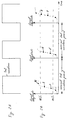
- FIG. 1 A block diagram of a single channel in a digital oscilloscope according to the present invention is shown in Fig. 1 while its operation will be explained on the basis of Figs. 2a-c. In order not to obscure the inventive concept, only selected elements are illustrated in the drawings. Since elements of the oscilloscope that are not shown in the drawings are well known to those skilled in the art, the description thereof will be omitted to avoid verbosity.
- Fig. 1 shows a signal generator 100 for generating a test waveform (the reference signal).
- the generated test waveform is a square-wave signal of a predetermined frequency which is not a multiple of the sampling rate of the digitizers. It is important that the frequency of the square-wave signal not be harmonically related to the sampling rate of the digitizers for the reason explained hereinbelow.
- each digitizer representatively includes a Sample-and-Hold (S/H) circuit for sampling the instantaneous signal voltage and for storing the samples to prevent ambiguity during the subsequent conversion if the signal voltage changes abruptly.
- S/H Sample-and-Hold
- A/D Analog-to-Digital
- the digital values produced by the A/D converter in each digitizer 104, 106 are stored in a memory unit 112 for subsequent processing by the system.
- the memory unit 112 is shown as a single element, it is understood that other embodiments of the present invention may include separate memory units for each digitizer, for example.
- the digitizers 104, 106 are driven by a clock signal generated by a time base circuit 108. Namely, each digitizer 104, 106 is activated by a signal from the time base circuit 108 as the interleaving of digital values supplied to the memory unit 112 is based on the clock signal alternately triggering the digitizers 104, 106. As mentioned above, the digitizers 104, 106 must be clocked at precise timing if a proper interleaving operation is to be carried out. As a result, it is necessary to perform a periodic calibration of the digitizers including the adjustment of clock signals.
- the clock signals may be delayed or advanced under control of a microprocessor 110, such as a central processing unit (CPU) or a programmable controller.
- the front end 102 is operative to select the square-wave signal (test waveform) generated by the signal generator 100 during the calibration procedure as shown in Fig. 2a.
- the square-wave signal has a rising edge of approximately 350 psec., 20% to 80% amplitude level, when the channel is in high impedance coupling; at least several hundred cycles of the test waveform are obtained for calibration.
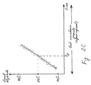
- Fig. 2b shows successive time periods of the theoretical (reference) test waveform and the digital representation of the actual test waveform as produced by the digitizers 104, 106.
- the top and base of the actual test waveform are determined by the microprocessor 110 using histogram techniques. To eliminate the effects of ringing or unsettled signal, only digital values within an amplitude range of 20-80% are selected from the actual test waveform. As shown in Fig. 2b, digital values 2, 3 from one period of the test waveform are selected by the microprocessor 110, while digital values 1, 4 are rejected. Similarly, digital values 5, 6, 7, 8, etc. are extracted during the subsequent periods of the test waveform.
- the microprocessor 110 calculates the relative delays of the digitizers 104, 106 with respect to the theoretical test waveform periods as illustrated in Fig. 2b.
- the extracted digital values with the corresponding test waveform cycle are maintained by the microprocessor 110.
- the period, slope and delay of each extracted digital value are calculated, and then the cycle number of the test waveform is subtracted from each digital value.
- all of the digital values are normalized (overlaid onto the edge as represented by a linear fit).
- the frequency of the square-wave signal should not be harmonically related to the sampling rate such that the reference signal has to slip phase relative to the sampling period of the digitizer. By observing this condition, the edge is populated evenly with samples (digital values).
- the above operation may be performed several times until the time delays stop converging. If, however, after several iterations as described hereinabove the time delays do not converge, the calibration may not be possible. In this situation, a display message indicating that the calibration procedure cannot be performed successfully is generated to notify the operator of the failed attempt.
- test waveform spans about 5 divisions on the oscilloscope when the front end is set to 50 mV/div. It is expected to be an approximately square-wave with a frequency of 14.31818 MHz and with a rise/fall time of 1 ns or less.
- the algorithm is designed to make use of either slope (but NOT both simultaneously), and the final choice is based on performance.
- the top and base of the calibration signal from each digitizer is found using histogram techniques. From this the 20%, 80% and median levels for each digitizer are computed. Ideally the gain and offsets already match, but finding separate levels insures that any remaining mismatch does not translate into a delay error.
- a single channel comprised of two digitizers was described and illustrated hereinabove. It is understood, of course, that more than two digitizers may be provided per channel, and more than one channel may be included in the digital oscilloscope.
- the rising edge of the test waveform was selected for the above illustrations of delay computations, the falling edge may be used just as well. That is, the above algorithm may utilize either a positive or negative slope of the test waveform.
- the above-described delay adjustment may be performed on a real-time basis to interleave the digitized output in each channel, as well as between channels.
- the calibration procedure may take place when there is a change in temperature or at various stages of the operation of the oscilloscope: power-up, user mode change, periodically, etc.
- the oscilloscope with the delay adjustment according to the present invention has resolution of better than 2 psec.
Abstract
Description
Y(k) where the index k runs over all points ON THE SLOPE for
the ADC i, 0<=k<K. K is the number of points which the ADC has on the slope. The algorithm for finding Y(k) includes following the acquired test waveform and retaining only those values which satisfy:
- j
- the sample number (j=0...number of points in record);
- n
- the number of iterations of the test signal;
= s * j
where
= (p+e)*n + d
where
- s, p are constants (an error in s is not very important, because s just provides the time scale)
- e, d are determined by the fit
- r = s*j-p*n
- E = A*e
- D = A*d
SR=SUM(k) {r * r} SN=SUM(k) {n * n}
NR=SUM(k) {n * r} YR=SUM(k) {Y(k) * r}
YN=SUM(k) {Y(k) * n}
R=SUM(k) { r } N=SUM(k) { n }
K=SUM(K) { l } Y=SUM(k) { Y(k) } Note that K is the number of (useful) data points.
SR' = SR - R*R/K NR' = NR - N*R/K
SN' = SN - N*N/K YR' = YR - Y*R/K
YN' = YN - Y*N/K
The solutions then are
- e = E/A =
- deviation from nominal pulse period, should be close to zero. The 4 values e(i) should be equal within a very small value.
- d = D/A =
- ADC time shift in nsec
Claims (14)
- Apparatus for performing calibration, comprising:a signal generator for generating a reference signal having a preselected period;a digitizer for digitizing said reference signal to produce a plurality of digitized values having respective amplitudes; anda programmable controller for obtaining, in each respective period, a temporal position of a digitized value with respect to a corresponding period of said reference signal, said programmable controller determining, based on the obtained temporal positions, a delay corresponding to an approximate median value of the amplitudes such that sampling times of said digitizer are adjusted on the basis of the determined delay.
- The apparatus according to claim 1, wherein prior to obtaining the temporal positions, said programmable controller selects the digitized values within a predetermined amplitude range.
- The apparatus according to claim 1, further comprising another digitizer for digitizing an input signal to produce digitized values that are interleaved with digitized values produced by the first-mentioned digitizer.
- The apparatus according to claim 1, further comprising a memory unit for storing the digitized values.
- The apparatus according to claim 1, further comprising a time base circuit for providing a clock signal to said digitizer to start a digitizing operation, said time base circuit being controlled by a control signal supplied by said programmable controller.
- The apparatus according to claim 5, wherein the timing of said clock signal is adjusted in response to the supplied control signal based on the determined delay.
- The apparatus according to claim 1, wherein said digitizer includes a sample-and-hold circuit and an analog-to-digital converter.
- The apparatus according to claim 1, wherein said reference signal is a square-wave signal.
- A digital oscilloscope with a self-calibration operation, comprising:an input port for receiving an input signal;a signal generator for generating a reference signal having a preselected period;a front end circuit for selecting one of said input and reference signals;a digitizer for selectively digitizing said input signal or said reference signal to produce a plurality of digitized values having respective amplitudes; anda programmable controller for obtaining, in each respective period, a temporal position of a digitized value of said reference signal with respect to a corresponding period of said reference signal, said programmable controller determining, based on the obtained temporal positions, a delay corresponding to an approximate median value of the amplitudes such that sampling times of said digitizer are adjusted on the basis of the determined delay.
- The apparatus according to claim 9, further comprising another digitizer for digitizing said input signal to produce digitized values that are interleaved with the digitized values of said input signal produced by the first-mentioned digitizer.
- The apparatus according to claim 10, further comprising a time base circuit for providing a clock signal to the digitizers to start a digitizing operation, said time base circuit being controlled by a control signal supplied by said programmable controller.
- The apparatus according to claim 11, wherein the timing of said clock signal is adjusted in response to the supplied control signal based on the determined delay.
- A method for performing calibration in a digital oscilloscope, comprising the steps of:receiving an input signal;generating a reference signal having a preselected period;selecting one of said input and reference signals;selectively digitizing said input signal or said reference signal to produce a plurality of digitized values having respective amplitudes;obtaining, in each respective period, a temporal position of a digitized value with respect to a corresponding period of said reference signal; anddetermining, based on the obtained temporal positions, a delay corresponding to an approximate median value of the amplitudes such that sampling times in said oscilloscope are adjusted on the basis of the determined delay.
- The method according to claim 13, further comprising the step of selecting the digitized values within a predetermined amplitude range prior to obtaining the temporal positions.
Applications Claiming Priority (2)
| Application Number | Priority Date | Filing Date | Title |
|---|---|---|---|
| US4430097P | 1997-04-30 | 1997-04-30 | |
| US44300P | 1997-04-30 |
Publications (3)
| Publication Number | Publication Date |
|---|---|
| EP0875764A2 true EP0875764A2 (en) | 1998-11-04 |
| EP0875764A3 EP0875764A3 (en) | 2000-06-28 |
| EP0875764B1 EP0875764B1 (en) | 2004-07-28 |
Family
ID=21931597
Family Applications (1)
| Application Number | Title | Priority Date | Filing Date |
|---|---|---|---|
| EP98303380A Expired - Lifetime EP0875764B1 (en) | 1997-04-30 | 1998-04-30 | Self-calibration of an oscilloscope using a square-wave test signal |
Country Status (6)
| Country | Link |
|---|---|
| US (1) | US6269317B1 (en) |
| EP (1) | EP0875764B1 (en) |
| JP (1) | JPH1144710A (en) |
| AT (1) | ATE272216T1 (en) |
| CA (1) | CA2236385C (en) |
| DE (1) | DE69825204T2 (en) |
Cited By (4)
| Publication number | Priority date | Publication date | Assignee | Title |
|---|---|---|---|---|
| EP1160797A1 (en) * | 2000-05-31 | 2001-12-05 | Texas Instruments Incorporated | A system and method for reducing timing mismatch in sample and hold circuits using the clock |
| EP1168368A1 (en) * | 2000-06-28 | 2002-01-02 | Texas Instruments Incorporated | A system and method for reducing timing msmatch in sample and hold circuits |
| EP1168367A1 (en) * | 2000-06-28 | 2002-01-02 | Texas Instruments Incorporated | A system and method for reducing timing mismatch in sample and hold circuits using an fft and subcircuit reassignment |
| CN105652104A (en) * | 2014-11-11 | 2016-06-08 | 江苏绿扬电子仪器集团有限公司 | Digital serial signal analyzer front channel self-correction apparatus and method |
Families Citing this family (50)
| Publication number | Priority date | Publication date | Assignee | Title |
|---|---|---|---|---|
| US6571186B1 (en) * | 1999-09-14 | 2003-05-27 | Textronix, Inc. | Method of waveform time stamping for minimizing digitization artifacts in time interval distribution measurements |
| US6775628B2 (en) * | 2001-11-27 | 2004-08-10 | Teradyne, Inc. | Low distortion frequency tracking technique |
| US7283917B2 (en) * | 2001-12-12 | 2007-10-16 | Alcatel Canada Inc. | System and method for calibrating an adjustable delay time for a delay module |
| US6919728B2 (en) * | 2002-02-27 | 2005-07-19 | Lecroy Corporation | Calibration cache and database |
| US6784819B2 (en) * | 2002-06-27 | 2004-08-31 | Teradyne, Inc. | Measuring skew between digitizer channels using fourier transform |
| DE10312208B3 (en) * | 2003-03-19 | 2004-07-01 | Lucas Automotive Gmbh | Counter for revolutions of wheel of road vehicle has sensor sending output signal to signal evaluation circuit with integrated circuit and main processor which monitor signal amplitude level |
| CA2484951A1 (en) * | 2004-09-27 | 2006-03-27 | Veris Industries, Llc | Method and apparatus for phase determination |
| WO2006075505A1 (en) * | 2005-01-11 | 2006-07-20 | Anritsu Corporation | Analog-to-digital converter device of improved time interleaving type, and high-speed signal processing system using the device |
| US7386409B2 (en) * | 2005-02-25 | 2008-06-10 | Lecroy Corporation | Method and apparatus for artifact signal reduction in systems of mismatched interleaved digitizers |
| US7183953B2 (en) * | 2005-03-31 | 2007-02-27 | Teradyne, Inc. | Calibrating automatic test equipment containing interleaved analog-to-digital converters |
| US7148828B2 (en) * | 2005-05-03 | 2006-12-12 | Agilent Technologies, Inc. | System and method for timing calibration of time-interleaved data converters |
| US20070036255A1 (en) * | 2005-08-09 | 2007-02-15 | Wolfe Robert T | Synchronization of data streams from data acquisition processors using a common signal |
| US7450043B2 (en) * | 2006-10-31 | 2008-11-11 | Lecroy Corporation | Method of compensating for deterministic jitter due to interleave error |
| CA2609611A1 (en) | 2007-09-10 | 2009-03-10 | Veris Industries, Llc | Split core status indicator |
| CA2609629A1 (en) | 2007-09-10 | 2009-03-10 | Veris Industries, Llc | Current switch with automatic calibration |
| CA2609619A1 (en) | 2007-09-10 | 2009-03-10 | Veris Industries, Llc | Status indicator |
| US8212548B2 (en) | 2008-06-02 | 2012-07-03 | Veris Industries, Llc | Branch meter with configurable sensor strip arrangement |
| US8446143B2 (en) * | 2008-06-27 | 2013-05-21 | National Instruments Corporation | Self-calibration circuit with gyrated output impedance |
| US8421443B2 (en) | 2008-11-21 | 2013-04-16 | Veris Industries, Llc | Branch current monitor with calibration |
| US8421639B2 (en) | 2008-11-21 | 2013-04-16 | Veris Industries, Llc | Branch current monitor with an alarm |
| US9335352B2 (en) | 2009-03-13 | 2016-05-10 | Veris Industries, Llc | Branch circuit monitor power measurement |
| CN101576610B (en) * | 2009-05-27 | 2012-01-11 | 秦轲 | Device and method for improving data sampling precision in oscillograph |
| EP2363961A1 (en) * | 2010-03-04 | 2011-09-07 | BAE SYSTEMS plc | Sampling |
| WO2011107801A1 (en) * | 2010-03-04 | 2011-09-09 | Bae Systems Plc | Sampling |
| US8788234B2 (en) * | 2010-10-15 | 2014-07-22 | Tektronix, Inc. | Method of calibrating interleaved digitizer channels |
| US9146264B2 (en) | 2011-02-25 | 2015-09-29 | Veris Industries, Llc | Current meter with on board memory |
| US10006948B2 (en) | 2011-02-25 | 2018-06-26 | Veris Industries, Llc | Current meter with voltage awareness |
| US9329996B2 (en) | 2011-04-27 | 2016-05-03 | Veris Industries, Llc | Branch circuit monitor with paging register |
| US9306590B2 (en) | 2011-05-26 | 2016-04-05 | Tektronix, Inc. | Test and measurement instrument including asynchronous time-interleaved digitizer using harmonic mixing |
| US9568503B2 (en) | 2011-05-26 | 2017-02-14 | Tektronix, Inc. | Calibration for test and measurement instrument including asynchronous time-interleaved digitizer using harmonic mixing |
| US9432042B2 (en) | 2011-05-26 | 2016-08-30 | Tektronix, Inc. | Test and measurement instrument including asynchronous time-interleaved digitizer using harmonic mixing |
| US9250308B2 (en) | 2011-06-03 | 2016-02-02 | Veris Industries, Llc | Simplified energy meter configuration |
| US8705677B2 (en) * | 2011-09-27 | 2014-04-22 | Teledyne Lecroy, Inc. | Multiple channel distributed system and method |
| US9410552B2 (en) | 2011-10-05 | 2016-08-09 | Veris Industries, Llc | Current switch with automatic calibration |
| US9886419B2 (en) * | 2012-07-26 | 2018-02-06 | Tektronix, Inc. | System for improving probability of transient event detection |
| JP6629511B2 (en) * | 2014-03-04 | 2020-01-15 | テクトロニクス・インコーポレイテッドTektronix,Inc. | Test measurement device and compensation value determination method |
| US9525427B1 (en) * | 2015-09-11 | 2016-12-20 | Tektronix, Inc. | Test and measurement instrument including asynchronous time-interleaved digitizer using harmonic mixing and a linear time-periodic filter |
| US10371730B2 (en) | 2015-12-28 | 2019-08-06 | Veris Industries, Llc | Branch current monitor with client level access |
| US10408911B2 (en) | 2015-12-28 | 2019-09-10 | Veris Industries, Llc | Network configurable system for a power meter |
| US10274572B2 (en) | 2015-12-28 | 2019-04-30 | Veris Industries, Llc | Calibration system for a power meter |
| US10371721B2 (en) | 2015-12-28 | 2019-08-06 | Veris Industries, Llc | Configuration system for a power meter |
| US11215650B2 (en) | 2017-02-28 | 2022-01-04 | Veris Industries, Llc | Phase aligned branch energy meter |
| US11193958B2 (en) | 2017-03-03 | 2021-12-07 | Veris Industries, Llc | Non-contact voltage sensor |
| US10705126B2 (en) | 2017-05-19 | 2020-07-07 | Veris Industries, Llc | Energy metering with temperature monitoring |
| CN107422203A (en) * | 2017-07-03 | 2017-12-01 | 中国电力科学研究院 | A kind of system and method for checking impulse current shunt |
| US11187726B2 (en) * | 2018-03-08 | 2021-11-30 | Rohde & Schwarz Gmbh & Co. Kg | Oscilloscope and method for operating an oscilloscope |
| US11558061B2 (en) | 2021-04-22 | 2023-01-17 | Ciena Corporation | ADC self-calibration with on-chip circuit and method |
| EP4183049A1 (en) * | 2021-04-22 | 2023-05-24 | Ciena Corporation | Adc self-calibration with on-chip circuit and method |
| CN113252958A (en) * | 2021-07-15 | 2021-08-13 | 深圳市鼎阳科技股份有限公司 | Digital oscilloscope and automatic calibration method for delay difference between channels thereof |
| CN117389128B (en) * | 2023-12-08 | 2024-02-23 | 深圳市山海半导体科技有限公司 | Automatic calibration method and system for digital clock |
Citations (7)
| Publication number | Priority date | Publication date | Assignee | Title |
|---|---|---|---|---|
| US4736189A (en) * | 1985-12-24 | 1988-04-05 | Sony/Tektronix Corporation | Method and apparatus for calibrating an analog-to-digital conversion apparatus |
| WO1988004059A1 (en) * | 1986-11-18 | 1988-06-02 | Gould Electronics Limited | A high speed sampling apparatus and method for calibrating the same |
| EP0298618A2 (en) * | 1987-07-08 | 1989-01-11 | Tektronix Inc. | Interleaved digitizer array with calibrated sample timing |
| US4843309A (en) * | 1988-03-21 | 1989-06-27 | Tektronix, Inc. | Waveform timing alignment system for digital oscilloscopes |
| US4962380A (en) * | 1989-09-21 | 1990-10-09 | Tektronix, Inc. | Method and apparatus for calibrating an interleaved digitizer |
| EP0554973A2 (en) * | 1992-01-31 | 1993-08-11 | Tektronix, Inc. | Multi-channel trigger dejitter |
| JPH09166623A (en) * | 1995-12-14 | 1997-06-24 | Hitachi Denshi Ltd | Sampling digitizer |
Family Cites Families (10)
| Publication number | Priority date | Publication date | Assignee | Title |
|---|---|---|---|---|
| JPS56115026A (en) | 1980-02-18 | 1981-09-10 | Sony Tektronix Corp | Analog-digital converter |
| US5055845A (en) | 1984-03-30 | 1991-10-08 | Datajet, Inc. | Signal digitizing method and system utilizing time delay of the input signal |
| US4627268A (en) | 1985-07-19 | 1986-12-09 | Hewlett-Packard Company | Method for calibrating instruments for time interval measurements |
| US5488369A (en) | 1986-11-18 | 1996-01-30 | Gould Electronics, Ltd. | High speed sampling apparatus and method for calibrating the same |
| US4768017A (en) | 1987-07-22 | 1988-08-30 | Sonotek, Inc. | Circuit for providing high sampling rate resolution using slow sampling rate |
| US4940931A (en) * | 1988-06-24 | 1990-07-10 | Anritsu Corporation | Digital waveform measuring apparatus having a shading-tone display function |
| US5239299A (en) | 1991-08-06 | 1993-08-24 | Trw Inc. | Digital equalization of time interleaved analog to digital converters |
| USD335093S (en) * | 1991-09-23 | 1993-04-27 | Snap-On Tools Corporation | Digital oscilloscope |
| US5621310A (en) * | 1994-07-15 | 1997-04-15 | Tektronix, Inc. | High frequency calibration circuit |
| US5521599A (en) | 1994-10-14 | 1996-05-28 | Tektronix, Inc. | High speed analog signal sampling system |
-
1998
- 1998-04-24 US US09/066,167 patent/US6269317B1/en not_active Expired - Lifetime
- 1998-04-29 CA CA002236385A patent/CA2236385C/en not_active Expired - Fee Related
- 1998-04-30 JP JP10120582A patent/JPH1144710A/en active Pending
- 1998-04-30 AT AT98303380T patent/ATE272216T1/en not_active IP Right Cessation
- 1998-04-30 DE DE69825204T patent/DE69825204T2/en not_active Expired - Fee Related
- 1998-04-30 EP EP98303380A patent/EP0875764B1/en not_active Expired - Lifetime
Patent Citations (7)
| Publication number | Priority date | Publication date | Assignee | Title |
|---|---|---|---|---|
| US4736189A (en) * | 1985-12-24 | 1988-04-05 | Sony/Tektronix Corporation | Method and apparatus for calibrating an analog-to-digital conversion apparatus |
| WO1988004059A1 (en) * | 1986-11-18 | 1988-06-02 | Gould Electronics Limited | A high speed sampling apparatus and method for calibrating the same |
| EP0298618A2 (en) * | 1987-07-08 | 1989-01-11 | Tektronix Inc. | Interleaved digitizer array with calibrated sample timing |
| US4843309A (en) * | 1988-03-21 | 1989-06-27 | Tektronix, Inc. | Waveform timing alignment system for digital oscilloscopes |
| US4962380A (en) * | 1989-09-21 | 1990-10-09 | Tektronix, Inc. | Method and apparatus for calibrating an interleaved digitizer |
| EP0554973A2 (en) * | 1992-01-31 | 1993-08-11 | Tektronix, Inc. | Multi-channel trigger dejitter |
| JPH09166623A (en) * | 1995-12-14 | 1997-06-24 | Hitachi Denshi Ltd | Sampling digitizer |
Non-Patent Citations (1)
| Title |
|---|
| PATENT ABSTRACTS OF JAPAN vol. 1997, no. 10, 31 October 1997 (1997-10-31) -& JP 09 166623 A (HITACHI DENSHI LTD), 24 June 1997 (1997-06-24) * |
Cited By (7)
| Publication number | Priority date | Publication date | Assignee | Title |
|---|---|---|---|---|
| EP1160797A1 (en) * | 2000-05-31 | 2001-12-05 | Texas Instruments Incorporated | A system and method for reducing timing mismatch in sample and hold circuits using the clock |
| US6518800B2 (en) | 2000-05-31 | 2003-02-11 | Texas Instruments Incorporated | System and method for reducing timing mismatch in sample and hold circuits using the clock |
| KR100889076B1 (en) * | 2000-05-31 | 2009-03-17 | 텍사스 인스트루먼츠 인코포레이티드 | A system and method for reducing timing mismatch in sample and hold circuits using the clock |
| EP1168368A1 (en) * | 2000-06-28 | 2002-01-02 | Texas Instruments Incorporated | A system and method for reducing timing msmatch in sample and hold circuits |
| EP1168367A1 (en) * | 2000-06-28 | 2002-01-02 | Texas Instruments Incorporated | A system and method for reducing timing mismatch in sample and hold circuits using an fft and subcircuit reassignment |
| US6483448B2 (en) | 2000-06-28 | 2002-11-19 | Texas Instruments Incorporated | System and method for reducing timing mismatch in sample and hold circuits using an FFT and decimation |
| CN105652104A (en) * | 2014-11-11 | 2016-06-08 | 江苏绿扬电子仪器集团有限公司 | Digital serial signal analyzer front channel self-correction apparatus and method |
Also Published As
| Publication number | Publication date |
|---|---|
| ATE272216T1 (en) | 2004-08-15 |
| EP0875764A3 (en) | 2000-06-28 |
| EP0875764B1 (en) | 2004-07-28 |
| CA2236385A1 (en) | 1998-10-30 |
| JPH1144710A (en) | 1999-02-16 |
| US6269317B1 (en) | 2001-07-31 |
| CA2236385C (en) | 2004-12-21 |
| DE69825204T2 (en) | 2005-07-21 |
| DE69825204D1 (en) | 2004-09-02 |
Similar Documents
| Publication | Publication Date | Title |
|---|---|---|
| EP0875764B1 (en) | Self-calibration of an oscilloscope using a square-wave test signal | |
| JP3805181B2 (en) | Time stamp addition method | |
| EP2574959B1 (en) | Time delay estimation | |
| US6956422B2 (en) | Generation and measurement of timing delays by digital phase error compensation | |
| US7856578B2 (en) | Strobe technique for test of digital signal timing | |
| JP2006313162A (en) | System and method for calibrating time interleaved timing of data converter | |
| US5886660A (en) | Time-to-digital converter using time stamp extrapolation | |
| CN106124033B (en) | Large-trigger-delay accumulated calibration method for laser vibration measurement calibration | |
| US7403274B2 (en) | Equivalent time sampling system | |
| JP2017040646A (en) | Test and measurement instrument and method of determining s-parameter | |
| US5578917A (en) | Repetitive digital sampling circuit using two delay lines for improved time accuracy | |
| US7184908B2 (en) | Calibration method of time measurement apparatus | |
| JPH056151B2 (en) | ||
| EP0191478A2 (en) | Measurement circuit for evaluating a digital-to-analog converter | |
| US20020136337A1 (en) | Method and apparatus for high-resolution jitter measurement | |
| US6411244B1 (en) | Phase startable clock device for a digitizing instrument having deterministic phase error correction | |
| US6998834B2 (en) | Real-time time drift adjustment for a TDR step stimulus | |
| CN107678333B (en) | Step length time correction method and device based on equivalent time sequence sampling | |
| Souders et al. | A wideband sampling voltmeter | |
| GB2440253A (en) | Optical time domain reflectometer employing an equivalent time sampling system | |
| CN113805042B (en) | Time delay measuring device and testing method | |
| Attivissimo et al. | Measuring time base distortion in analog-memory sampling digitizers | |
| RU2159446C1 (en) | Stroboscopic transducer calibration process | |
| JPH0328792A (en) | Automatic time interval measuring method | |
| SU877448A1 (en) | Device for determination of stroboscopic transducer graduation characteristics |
Legal Events
| Date | Code | Title | Description |
|---|---|---|---|
| PUAI | Public reference made under article 153(3) epc to a published international application that has entered the european phase |
Free format text: ORIGINAL CODE: 0009012 |
|
| AK | Designated contracting states |
Kind code of ref document: A2 Designated state(s): AT BE CH CY DE DK ES FI FR GB GR IE IT LI LU MC NL PT SE |
|
| AX | Request for extension of the european patent |
Free format text: AL;LT;LV;MK;RO;SI |
|
| PUAL | Search report despatched |
Free format text: ORIGINAL CODE: 0009013 |
|
| AK | Designated contracting states |
Kind code of ref document: A3 Designated state(s): AT BE CH CY DE DK ES FI FR GB GR IE IT LI LU MC NL PT SE |
|
| AX | Request for extension of the european patent |
Free format text: AL;LT;LV;MK;RO;SI |
|
| 17P | Request for examination filed |
Effective date: 20001205 |
|
| AKX | Designation fees paid |
Free format text: AT BE CH CY DE DK ES FI FR GB GR IE IT LI LU MC NL PT SE |
|
| 17Q | First examination report despatched |
Effective date: 20020315 |
|
| GRAP | Despatch of communication of intention to grant a patent |
Free format text: ORIGINAL CODE: EPIDOSNIGR1 |
|
| GRAS | Grant fee paid |
Free format text: ORIGINAL CODE: EPIDOSNIGR3 |
|
| GRAA | (expected) grant |
Free format text: ORIGINAL CODE: 0009210 |
|
| AK | Designated contracting states |
Kind code of ref document: B1 Designated state(s): AT BE CH CY DE DK ES FI FR GB GR IE IT LI LU MC NL PT SE |
|
| PG25 | Lapsed in a contracting state [announced via postgrant information from national office to epo] |
Ref country code: NL Free format text: LAPSE BECAUSE OF FAILURE TO SUBMIT A TRANSLATION OF THE DESCRIPTION OR TO PAY THE FEE WITHIN THE PRESCRIBED TIME-LIMIT Effective date: 20040728 Ref country code: IT Free format text: LAPSE BECAUSE OF FAILURE TO SUBMIT A TRANSLATION OF THE DESCRIPTION OR TO PAY THE FEE WITHIN THE PRE;WARNING: LAPSES OF ITALIAN PATENTS WITH EFFECTIVE DATE BEFORE 2007 MAY HAVE OCCURRED AT ANY TIME BEFORE 2007. THE CORRECT EFFECTIVE DATE MAY BE DIFFERENT FROM THE ONE RECORDED.SCRIBED TIME-LIMIT Effective date: 20040728 Ref country code: FI Free format text: LAPSE BECAUSE OF FAILURE TO SUBMIT A TRANSLATION OF THE DESCRIPTION OR TO PAY THE FEE WITHIN THE PRESCRIBED TIME-LIMIT Effective date: 20040728 Ref country code: BE Free format text: LAPSE BECAUSE OF FAILURE TO SUBMIT A TRANSLATION OF THE DESCRIPTION OR TO PAY THE FEE WITHIN THE PRESCRIBED TIME-LIMIT Effective date: 20040728 Ref country code: AT Free format text: LAPSE BECAUSE OF FAILURE TO SUBMIT A TRANSLATION OF THE DESCRIPTION OR TO PAY THE FEE WITHIN THE PRESCRIBED TIME-LIMIT Effective date: 20040728 |
|
| REG | Reference to a national code |
Ref country code: GB Ref legal event code: FG4D |
|
| REG | Reference to a national code |
Ref country code: CH Ref legal event code: EP |
|
| REG | Reference to a national code |
Ref country code: CH Ref legal event code: NV Representative=s name: ISLER & PEDRAZZINI AG |
|
| REG | Reference to a national code |
Ref country code: IE Ref legal event code: FG4D |
|
| REF | Corresponds to: |
Ref document number: 69825204 Country of ref document: DE Date of ref document: 20040902 Kind code of ref document: P |
|
| PG25 | Lapsed in a contracting state [announced via postgrant information from national office to epo] |
Ref country code: SE Free format text: LAPSE BECAUSE OF FAILURE TO SUBMIT A TRANSLATION OF THE DESCRIPTION OR TO PAY THE FEE WITHIN THE PRESCRIBED TIME-LIMIT Effective date: 20041028 Ref country code: GR Free format text: LAPSE BECAUSE OF FAILURE TO SUBMIT A TRANSLATION OF THE DESCRIPTION OR TO PAY THE FEE WITHIN THE PRESCRIBED TIME-LIMIT Effective date: 20041028 Ref country code: DK Free format text: LAPSE BECAUSE OF FAILURE TO SUBMIT A TRANSLATION OF THE DESCRIPTION OR TO PAY THE FEE WITHIN THE PRESCRIBED TIME-LIMIT Effective date: 20041028 |
|
| PG25 | Lapsed in a contracting state [announced via postgrant information from national office to epo] |
Ref country code: ES Free format text: LAPSE BECAUSE OF FAILURE TO SUBMIT A TRANSLATION OF THE DESCRIPTION OR TO PAY THE FEE WITHIN THE PRESCRIBED TIME-LIMIT Effective date: 20041108 |
|
| NLV1 | Nl: lapsed or annulled due to failure to fulfill the requirements of art. 29p and 29m of the patents act | ||
| ET | Fr: translation filed | ||
| PG25 | Lapsed in a contracting state [announced via postgrant information from national office to epo] |
Ref country code: MC Free format text: LAPSE BECAUSE OF NON-PAYMENT OF DUE FEES Effective date: 20050430 Ref country code: LU Free format text: LAPSE BECAUSE OF NON-PAYMENT OF DUE FEES Effective date: 20050430 Ref country code: CY Free format text: LAPSE BECAUSE OF FAILURE TO SUBMIT A TRANSLATION OF THE DESCRIPTION OR TO PAY THE FEE WITHIN THE PRESCRIBED TIME-LIMIT Effective date: 20050430 |
|
| PG25 | Lapsed in a contracting state [announced via postgrant information from national office to epo] |
Ref country code: IE Free format text: LAPSE BECAUSE OF NON-PAYMENT OF DUE FEES Effective date: 20050502 |
|
| PLBE | No opposition filed within time limit |
Free format text: ORIGINAL CODE: 0009261 |
|
| STAA | Information on the status of an ep patent application or granted ep patent |
Free format text: STATUS: NO OPPOSITION FILED WITHIN TIME LIMIT |
|
| 26N | No opposition filed |
Effective date: 20050429 |
|
| REG | Reference to a national code |
Ref country code: IE Ref legal event code: MM4A |
|
| PGFP | Annual fee paid to national office [announced via postgrant information from national office to epo] |
Ref country code: CH Payment date: 20070427 Year of fee payment: 10 |
|
| PGFP | Annual fee paid to national office [announced via postgrant information from national office to epo] |
Ref country code: DE Payment date: 20070531 Year of fee payment: 10 |
|
| REG | Reference to a national code |
Ref country code: CH Ref legal event code: PCAR Free format text: ISLER & PEDRAZZINI AG;POSTFACH 1772;8027 ZUERICH (CH) |
|
| PGFP | Annual fee paid to national office [announced via postgrant information from national office to epo] |
Ref country code: GB Payment date: 20070425 Year of fee payment: 10 |
|
| PG25 | Lapsed in a contracting state [announced via postgrant information from national office to epo] |
Ref country code: PT Free format text: LAPSE BECAUSE OF NON-PAYMENT OF DUE FEES Effective date: 20041228 |
|
| PGFP | Annual fee paid to national office [announced via postgrant information from national office to epo] |
Ref country code: FR Payment date: 20070417 Year of fee payment: 10 |
|
| REG | Reference to a national code |
Ref country code: CH Ref legal event code: PL |
|
| GBPC | Gb: european patent ceased through non-payment of renewal fee |
Effective date: 20080430 |
|
| PG25 | Lapsed in a contracting state [announced via postgrant information from national office to epo] |
Ref country code: LI Free format text: LAPSE BECAUSE OF NON-PAYMENT OF DUE FEES Effective date: 20080430 Ref country code: DE Free format text: LAPSE BECAUSE OF NON-PAYMENT OF DUE FEES Effective date: 20081101 Ref country code: CH Free format text: LAPSE BECAUSE OF NON-PAYMENT OF DUE FEES Effective date: 20080430 |
|
| REG | Reference to a national code |
Ref country code: FR Ref legal event code: ST Effective date: 20081231 |
|
| PG25 | Lapsed in a contracting state [announced via postgrant information from national office to epo] |
Ref country code: FR Free format text: LAPSE BECAUSE OF NON-PAYMENT OF DUE FEES Effective date: 20080430 |
|
| PG25 | Lapsed in a contracting state [announced via postgrant information from national office to epo] |
Ref country code: GB Free format text: LAPSE BECAUSE OF NON-PAYMENT OF DUE FEES Effective date: 20080430 |