EP0865153B1 - Variable load inductance compensation for motor drive circuits - Google Patents
Variable load inductance compensation for motor drive circuits Download PDFInfo
- Publication number
- EP0865153B1 EP0865153B1 EP98400549A EP98400549A EP0865153B1 EP 0865153 B1 EP0865153 B1 EP 0865153B1 EP 98400549 A EP98400549 A EP 98400549A EP 98400549 A EP98400549 A EP 98400549A EP 0865153 B1 EP0865153 B1 EP 0865153B1
- Authority
- EP
- European Patent Office
- Prior art keywords
- inductance
- amplifier
- motor
- inductance compensation
- core
- Prior art date
- Legal status (The legal status is an assumption and is not a legal conclusion. Google has not performed a legal analysis and makes no representation as to the accuracy of the status listed.)
- Expired - Lifetime
Links
- 230000004044 response Effects 0.000 claims description 27
- 230000003321 amplification Effects 0.000 claims description 21
- 238000003199 nucleic acid amplification method Methods 0.000 claims description 21
- 229920006395 saturated elastomer Polymers 0.000 claims description 15
- 238000012544 monitoring process Methods 0.000 claims description 11
- 238000000034 method Methods 0.000 claims description 7
- 230000003247 decreasing effect Effects 0.000 claims description 3
- 230000008878 coupling Effects 0.000 claims description 2
- 238000010168 coupling process Methods 0.000 claims description 2
- 238000005859 coupling reaction Methods 0.000 claims description 2
- 239000003990 capacitor Substances 0.000 description 8
- 230000008859 change Effects 0.000 description 8
- 230000010355 oscillation Effects 0.000 description 5
- 238000010586 diagram Methods 0.000 description 3
- 230000002411 adverse Effects 0.000 description 2
- 230000007423 decrease Effects 0.000 description 2
- 230000007246 mechanism Effects 0.000 description 2
- 230000036961 partial effect Effects 0.000 description 2
- 230000002829 reductive effect Effects 0.000 description 2
- 230000008901 benefit Effects 0.000 description 1
- 238000001514 detection method Methods 0.000 description 1
- 230000006698 induction Effects 0.000 description 1
- 230000000670 limiting effect Effects 0.000 description 1
- 230000004048 modification Effects 0.000 description 1
- 238000012986 modification Methods 0.000 description 1
- 230000003287 optical effect Effects 0.000 description 1
Images



Classifications
-
- H—ELECTRICITY
- H02—GENERATION; CONVERSION OR DISTRIBUTION OF ELECTRIC POWER
- H02P—CONTROL OR REGULATION OF ELECTRIC MOTORS, ELECTRIC GENERATORS OR DYNAMO-ELECTRIC CONVERTERS; CONTROLLING TRANSFORMERS, REACTORS OR CHOKE COILS
- H02P25/00—Arrangements or methods for the control of AC motors characterised by the kind of AC motor or by structural details
- H02P25/02—Arrangements or methods for the control of AC motors characterised by the kind of AC motor or by structural details characterised by the kind of motor
- H02P25/08—Reluctance motors
-
- H—ELECTRICITY
- H02—GENERATION; CONVERSION OR DISTRIBUTION OF ELECTRIC POWER
- H02P—CONTROL OR REGULATION OF ELECTRIC MOTORS, ELECTRIC GENERATORS OR DYNAMO-ELECTRIC CONVERTERS; CONTROLLING TRANSFORMERS, REACTORS OR CHOKE COILS
- H02P25/00—Arrangements or methods for the control of AC motors characterised by the kind of AC motor or by structural details
- H02P25/16—Arrangements or methods for the control of AC motors characterised by the kind of AC motor or by structural details characterised by the circuit arrangement or by the kind of wiring
- H02P25/24—Variable impedance in stator or rotor circuit
-
- H—ELECTRICITY
- H02—GENERATION; CONVERSION OR DISTRIBUTION OF ELECTRIC POWER
- H02P—CONTROL OR REGULATION OF ELECTRIC MOTORS, ELECTRIC GENERATORS OR DYNAMO-ELECTRIC CONVERTERS; CONTROLLING TRANSFORMERS, REACTORS OR CHOKE COILS
- H02P7/00—Arrangements for regulating or controlling the speed or torque of electric DC motors
- H02P7/06—Arrangements for regulating or controlling the speed or torque of electric DC motors for regulating or controlling an individual DC dynamo-electric motor by varying field or armature current
- H02P7/18—Arrangements for regulating or controlling the speed or torque of electric DC motors for regulating or controlling an individual DC dynamo-electric motor by varying field or armature current by master control with auxiliary power
- H02P7/24—Arrangements for regulating or controlling the speed or torque of electric DC motors for regulating or controlling an individual DC dynamo-electric motor by varying field or armature current by master control with auxiliary power using discharge tubes or semiconductor devices
- H02P7/28—Arrangements for regulating or controlling the speed or torque of electric DC motors for regulating or controlling an individual DC dynamo-electric motor by varying field or armature current by master control with auxiliary power using discharge tubes or semiconductor devices using semiconductor devices
- H02P7/285—Arrangements for regulating or controlling the speed or torque of electric DC motors for regulating or controlling an individual DC dynamo-electric motor by varying field or armature current by master control with auxiliary power using discharge tubes or semiconductor devices using semiconductor devices controlling armature supply only
- H02P7/288—Arrangements for regulating or controlling the speed or torque of electric DC motors for regulating or controlling an individual DC dynamo-electric motor by varying field or armature current by master control with auxiliary power using discharge tubes or semiconductor devices using semiconductor devices controlling armature supply only using variable impedance
Definitions
- the invention relates to motor control circuits and, in particular, to an improved circuit for dynamic inductance compensation of a motor drive circuit.
- the load inductance range may only be changed manually by substituting one or more inductance compensation values, e.g., one or more capacitors and/or resistors.
- the predetermined inductance compensation value allows the servo amplifier to operate over one inductance range at any given time.
- the above-described arrangement works well for motors which have a limited or constant load-inductance range.
- the above-described arrangement works well for permanent magnet servo motors which operate in the linear characteristic region of the magnetic, e.g., in a region below magnetic saturation of the core.
- Fig. 5 shows the step response of a servo amplifier (i.e., a Model 432 DC Brush Servo Amplifier from Copley Controls Corporation, Westwood, MA) configured with an inductance compensation resistor of 200 k ⁇ and operated with a switched reluctance motor.
- a servo amplifier i.e., a Model 432 DC Brush Servo Amplifier from Copley Controls Corporation, Westwood, MA
- the 200 k ⁇ inductance compensation resistor is suitable for operation of a motor in the unsaturated inductance condition, at current values above the saturation point, the low inductance is not compensated properly.
- the voltage step of the amplifier input 100 results in a voltage step at the motor coil current 101 displaying oscillations.
- Fig. 6 shows the amplifier step response with the induction compensation resistor, e.g ., an 18 k ⁇ resistor selected for operation with a saturated inductance.
- the induction compensation resistor e.g ., an 18 k ⁇ resistor selected for operation with a saturated inductance.
- an 18 k ⁇ inductance compensation resistor eliminates the above-described oscillations, the rise time response of the motor coil current 102 is adversely affected.
- the rise time response of the servo amplifier, configured with the 18 k ⁇ inductance compensation resistor is approximately twice the rise time associated with the amplifier configured with the 200 k ⁇ inductance compensation resistor.
- the oscillations may be prevented by reducing the value of the inductance compensation components, motor performance is adversely affected such that the maximum motor speed for a given motor force is reduced by a factor proportional to the increase in the rise time. Accordingly, conventional arrangements for inductance compensation of commercially available servo amplifiers are unsatisfactory.
- US Patent US 4 595 865 describes an apparatus which, as the apparatus of the invention, comprises a motor and an amplifier coupled to the motor, the motor having a core and a coil disposed about the core and being configured for operating with a first inductance value when the core is in a saturated condition and with a second inductance value when the core is in a non-saturated condition, and the amplifier including means for supplying a controlled drive current to the motor,
- Objects of the invention include providing an apparatus and a method for configuring and operating servo amplifiers to improve the performance of motors which have a variable inductance.
- the apparatus of the invention is mainly characterized in that said amplifier further includes means for monitoring inductance variations of the coil and an inductance compensation circuit for providing inductance compensation, and in that said inductance compensation circuit includes switching means for switching between at least first and second inductance compensation values in response to predetermined coil inductance variations.
- the apparatus of the invention includes a load (such as a switch-reluctance motor) having first and second inductance values.
- a servo amplifier is coupled to and drives the load.
- the servo amplifier has an inductance compensation circuit which varies the drive characteristics of the servo amplifier in accordance with variations in the inductance value of the load.
- the inductance compensation circuit may vary the drive characteristics of the amplifier by monitoring the current in the motor coil.
- the amplifier preferably includes a current monitor output and a load inductance compensation control input, the switching means being coupled to and controlled by the current monitor output for alternately applying the first and second inductance compensation values to the load-inductance compensation control input.
- the means for monitoring inductance variations in the core includes means for monitoring the current in the coil.
- the amplifier may vary an amount of amplification in response to the core being in a saturated condition.
- the inductance compensation circuit is responsive to the motor having inductance variations, includes at least two inductance compensation values, and further includes switching means for alternately coupling and decoupling at least one of the inductance compensation values from the inductance compensation circuit.
- the amplifier may include a current monitor output, the first inductance compensation value being connected to the inductance compensation control input in response to the current monitor output having a first value and disconnected from the inductance compensation control input in response to the current monitor output having a second value different from the first value.
- the invention also relates to a method for supplying a motor having a coil and a core operating either in a saturated or in a non-saturated condition, said method comprising the step of supplying a controlled drive current to the motor through an amplifier and being characterized in that it further comprises the steps of detecting a saturation condition in the core of the motor, and adapting the amplification of the amplifier to the saturation condition detected.
- adapting the amplification of the amplifier includes alternately switching between at least first and second amplification values of the amplifier in a feedback control system for driving the motor in response to variations in the inductance of said motor.
- adapting the amplification of the amplifier includes decreasing the amplification of said amplifier when the core of the motor is in a saturation condition.
- a variable reactance motor control system 1 may include a amplifier 2, e.g., a servo amplifier/motor drive circuit, coupled to an inductance compensation circuit 4.
- the amplifier 2 is most preferably a Model 432 DC Brush Servo Amplifier from Copley Controls Corporation.
- the amplifier 2 is preferably coupled to a motor 3.
- the motor 3 may be variously configured.
- the motor 3 may include any suitable arrangement where the motor operates with a phase inductance which varies widely.
- the motor 3 includes a switch reluctance motor.
- the inductance compensation circuit 4 is coupled to the amplifier 2 to dynamically vary the response characteristics of the amplifier 2 in response to changes in the reactance of the motor 3.
- the amplifier 2 may be variously configured, in the most preferred embodiments, the amplifier 2 includes a current monitor output 6 responsive to the output current of the amplifier 2.
- the amplifier 2 may also include a positive reference voltage V+ and a negative reference voltage V-. In the most preferred embodiments, the positive reference voltage V+ is set at approximately positive 15 volts, and the negative reference voltage V- is set at approximately negative 15 volts.
- the amplifier 2 most preferably includes one or more inductance compensation inputs I1 and I2. In the most preferred embodiments, the inductance compensation inputs adjust the amplifier and/or driver output 7 to compensate for different core inductances in the motor 3.
- the inductance compensation circuit 4 is shown separately from amplifier 2, it may also be incorporated into the amplifier assembly.
- first and second comparators C1, C2 are utilized to discriminate between a saturated and an unsaturated operating condition of motor 3.
- the current monitor output 6 of the amplifier 2 may be input into the negative input of comparator C1 and into the positive input of comparator C2.
- a voltage divider comprising resistors R1, R2, and R3, connected between the positive reference voltage V+ and the negative reference voltage V-, supplies fixed reference voltages to the comparators.
- node N1, between resistors R2 and R3 provides the negative input to comparator C2
- node N2, between resistors R1 and R2 provides the positive input to comparator C1.
- the voltage divider may be variously configured, but, in the most preferred embodiment, is set such that the voltage at node N2 is a positive two volts and the voltage at N1 is a negative two volts.
- the output of comparators C1 and C2 is preferably configured as an open collector output and coupled together at node N3.
- the output at node N3 is then fed back into amplifier 2, via a switch 31, controlling the impedance input at the load-inductance compensation inputs I1 and I2.
- switch 31 controls the resistance applied to the load-inductance compensation inputs I1, I2.
- resistors R4 and R5 may be selectively coupled in parallel via optocoupler switch T1.
- R4 may be 200 K ⁇ and R5 may be 18 K ⁇ . Accordingly, the impedance of the load-inductance compensation input may be varied by switching transistor T1 on and off.
- resistors are shown for exemplary purposes, any capacitance and/or resistance network may be utilized, either in addition to or instead of the illustrated resistance network. Further, other inductance modification circuits will be apparent to those skilled in the art.
- resistor R4 is matched to provide optimal inductance compensation for a motor operated in an unsaturated phase inductance, i.e., at a low current below the core saturation point.
- resistor R5 is matched for optimum performance of the amplifier 2 for the saturated phase inductance condition for current values above the core saturation point.
- the amplifier 2 drives the motor 3, with the current monitor signal from amplifier 2 being proportional to the phase current delivered to the motor 3.
- the voltage of the current monitor output also increases proportionally.
- the voltage at the comparator outputs drops to the negative voltage bias position, e.g ., -15 volts.
- switch 31 is activated, switching resistor R5 in parallel with resistor R4.
- the load-inductance compensation resistor is reduced by approximately an order of magnitude.
- Figs. 2a-2c shows an example where the resistor R4 is set to be 200 k ⁇ and resistor R5 is set to be 18 k ⁇ . At current values below the core saturation range, switch 31 is turned off and the load-inductance compensation resistor is again controlled by resistor R4.
- the output current 103 response for the circuits of Fig. 1 is significantly improved over the output current 101 and 102 response obtained in Figs. 5 and 6 .
- the oscillations present in Fig. 5 are eliminated, and the slow response time shown in Fig. 6 is also eliminated.
- the dynamic response of the control system shown in Fig. 1 is significantly improved over the response of the conventional control system shown in Figs. 5 and 6 .
- Fig. 4 shows the embodiment of the present invention in block diagram form, including the amplifier circuitry.
- Motor 3 is driven by a pulse width modulator (PWM) 22.
- the pulse width modulator 22 is controlled by the output of current error amp 21.
- the pulse width modulator 22 also outputs a current monitor signal which has a voltage proportional to a current in the motor 3.
- the current monitor signal may be obtained by measuring a voltage across a resistor connected in parallel and/or series with motor 3.
- the current monitor signal may then be fed back into current error amplifier 21 and compared with a current reference signal.
- the difference between the current reference signal and the current monitor signal may be amplified by amplifier 21 and output back into the pulse width modulator 22 to complete the feedback loop.
- the amplification factor of current error amplifier 21 is controlled by a feedback circuit, e.g., feedback circuit A 42 and feedback circuit B 43.
- Switch 44 controls two or more feedback control circuits disposed in conjunction with current error amplifier 21.
- Inductance change detector 41 determines when the inductance of the motor has changed.
- the inductance change detector 41 is most preferably operated with a motor where the inductance changes between two distinct states, e.g., a saturated core condition and an unsaturated core condition.
- the inductance change detector 41 controls switch 44 to alternatingly switch in and out feedback network A or B in response to changes in the inductance of motor 3.
- Feedback circuits A and B may be variously configured to include any suitable feedback control arrangement.
- feedback circuits A and B comprise a resistor and capacitor coupled in a series circuit which is, in turn, coupled in parallel with a bypass capacitor.
- feedback circuit A comprises a 200 k ⁇ resistor coupled in series with a 47nF capacitor to form a series circuit which is, in turn, coupled in parallel with a 470pF capacitor.
- feedback circuit B comprises an 18 k ⁇ resistor coupled in series with a 47nF capacitor to form a series circuit which is, in turn, coupled in parallel with a 470pF capacitor.
- Various other feedback arrangements will be apparent to those skilled in the art.
- An advantage of the two step feedback control arrangement is that the amplification of the amplifier can be closely tailored to meet the requirements of motors, such as linear motors, which switch between first and second inductance states.
- the switch feedback arrangement has been found to be particularly effective in optimizing the motor drive circuits in linear motors.
- the current error amplifier 21 may be any suitable arrangement. In the most preferred embodiments, the current error amplifier 21 may be configured in the same manner as the current error amplifier shown in Copley Controls Corporation's Model 432 DC Brush Servo Amplifier.
- the speed control 23 may be any suitable speed control which provides a current reference output.
- the inductance change detector 41 may be configured as shown in Fig. 1 and may include the first and second comparators C1, C2 and the voltage divider comprising resistors R1-R3. Alternatively, the inductance change detector 41 may comprise any suitable detection mechanism (including an optical or magnetic sensor) which outputs a signal that varies in accordance with inductance changes in motor 3.
- Switch 44 may switch between two alternate feedback circuits, or it may be configured to switch in or out one or more inductance-compensation components in a single feedback circuit, as shown in Fig. 1 .
- the switch 44 in conjunction with feedback circuits A and B, forms a dynamic inductance compensation circuit.
- Inductance change detector 41 forms a means for monitoring inductance variations.
- the monitoring means may be an external sensor.
- a second amplifier may be alternatingly switched with a first amplifier. Further, the inductance compensation may occur directly in the pulse width modulator circuit 22.
- the embodiments of the invention switch between two amplification values to optimize the feedback control system for a switched reluctance motor.
- an increase in the gain of the current error amplifier 21 produces a larger voltage across the load, decreasing the response time of the control system.
- the rate of change of current in an inductor in the motor 3 is proportional to the voltage across the inductance. Accordingly, as the inductance changes to the lower value, the motor control system 1 switches to the lower amplification factor to decrease the voltage across the inductor.
- the load-inductance compensation circuit may be variously configured to include any parallel and/or serial connection of resistors and capacitors, coupled in an appropriate way to a suitable amplifier and/or motor-driving circuit.
- the circuit monitoring changes in the motor 3 are not limited to the current monitor circuit, and may include any number of monitoring mechanisms and suitable control logic for controlling switch 31.
- switch 31 may be configured in any number of ways well known to those skilled in the art.
Landscapes
- Engineering & Computer Science (AREA)
- Power Engineering (AREA)
- Control Of Electric Motors In General (AREA)
- Control Of Direct Current Motors (AREA)
- Synchronous Machinery (AREA)
Description
- The invention relates to motor control circuits and, in particular, to an improved circuit for dynamic inductance compensation of a motor drive circuit.
- Conventionally, commercially available servo amplifiers operate properly over a limited-load inductance range. Typically, the load inductance range may only be changed manually by substituting one or more inductance compensation values, e.g., one or more capacitors and/or resistors. The predetermined inductance compensation value allows the servo amplifier to operate over one inductance range at any given time. The above-described arrangement works well for motors which have a limited or constant load-inductance range. For example, the above-described arrangement works well for permanent magnet servo motors which operate in the linear characteristic region of the magnetic, e.g., in a region below magnetic saturation of the core. However, a problem arises in motors which operate both in a region where the cores are in magnetic saturation and where the cores are not in saturation or in motors where the inductance varies widely, e.g., in switch-reluctance motors.
- Referring to
Figs. 5 and 6 , it can be demonstrated that the step response of commercially available, single-load range, servo amplifiers is unsatisfactory when utilized with variable reluctance motors. Specifically,Fig. 5 shows the step response of a servo amplifier (i.e., a Model 432 DC Brush Servo Amplifier from Copley Controls Corporation, Westwood, MA) configured with an inductance compensation resistor of 200 kΩ and operated with a switched reluctance motor. Although the 200 kΩ inductance compensation resistor is suitable for operation of a motor in the unsaturated inductance condition, at current values above the saturation point, the low inductance is not compensated properly. In this configuration, as shown inFig. 5 , the voltage step of theamplifier input 100 results in a voltage step at themotor coil current 101 displaying oscillations. - Similarly,
Fig. 6 shows the amplifier step response with the induction compensation resistor, e.g., an 18 kΩ resistor selected for operation with a saturated inductance. Although an 18 kΩ inductance compensation resistor eliminates the above-described oscillations, the rise time response of themotor coil current 102 is adversely affected. For example, the rise time response of the servo amplifier, configured with the 18 kΩ inductance compensation resistor, is approximately twice the rise time associated with the amplifier configured with the 200 kΩ inductance compensation resistor. Although the oscillations may be prevented by reducing the value of the inductance compensation components, motor performance is adversely affected such that the maximum motor speed for a given motor force is reduced by a factor proportional to the increase in the rise time. Accordingly, conventional arrangements for inductance compensation of commercially available servo amplifiers are unsatisfactory. - US Patent
US 4 595 865 describes an apparatus which, as the apparatus of the invention, comprises a motor and an amplifier coupled to the motor, the motor having a core and a coil disposed about the core and being configured for operating with a first inductance value when the core is in a saturated condition and with a second inductance value when the core is in a non-saturated condition, and the amplifier including means for supplying a controlled drive current to the motor, - Objects of the invention include providing an apparatus and a method for configuring and operating servo amplifiers to improve the performance of motors which have a variable inductance.
- To this purpose, the apparatus of the invention is mainly characterized in that said amplifier further includes means for monitoring inductance variations of the coil and an inductance compensation circuit for providing inductance compensation, and in that said inductance compensation circuit includes switching means for switching between at least first and second inductance compensation values in response to predetermined coil inductance variations.
- More specifically, the apparatus of the invention includes a load (such as a switch-reluctance motor) having first and second inductance values. A servo amplifier is coupled to and drives the load. The servo amplifier has an inductance compensation circuit which varies the drive characteristics of the servo amplifier in accordance with variations in the inductance value of the load. The inductance compensation circuit may vary the drive characteristics of the amplifier by monitoring the current in the motor coil.
- Thus, the amplifier preferably includes a current monitor output and a load inductance compensation control input, the switching means being coupled to and controlled by the current monitor output for alternately applying the first and second inductance compensation values to the load-inductance compensation control input.
- For instance, the means for monitoring inductance variations in the core includes means for monitoring the current in the coil.
- Typically, the amplifier may vary an amount of amplification in response to the core being in a saturated condition.
- For instance, the inductance compensation circuit is responsive to the motor having inductance variations, includes at least two inductance compensation values, and further includes switching means for alternately coupling and decoupling at least one of the inductance compensation values from the inductance compensation circuit.
- The amplifier may include a current monitor output, the first inductance compensation value being connected to the inductance compensation control input in response to the current monitor output having a first value and disconnected from the inductance compensation control input in response to the current monitor output having a second value different from the first value.
- The invention also relates to a method for supplying a motor having a coil and a core operating either in a saturated or in a non-saturated condition, said method comprising the step of supplying a controlled drive current to the motor through an amplifier and being characterized in that it further comprises the steps of detecting a saturation condition in the core of the motor, and adapting the amplification of the amplifier to the saturation condition detected.
- For instance, adapting the amplification of the amplifier includes alternately switching between at least first and second amplification values of the amplifier in a feedback control system for driving the motor in response to variations in the inductance of said motor.
- Typically, adapting the amplification of the amplifier includes decreasing the amplification of said amplifier when the core of the motor is in a saturation condition.
-
-
Fig. 1 is a partial circuit and partial block diagram of a servo amplifier coupled to a motor and a dynamic inductance compensation circuit; -
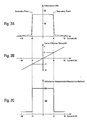
Figs.2a-2c , respectively, illustrate motor coil inductance, current monitor output voltage, and load-inductance compensation resistance as a function of coil/motor current; -
Fig. 3 shows a step response of a servo amplifier configured with a dynamic inductance compensation circuit in accordance with the present invention; -
Fig. 4 is a block diagram of a variable reluctance motor control system in accordance with aspects of the present invention; -
Fig. 5 is a graphic representation of a step response of a servo amplifier compensated with a resistor selected for operation in an unsaturated inductance region; and -
Fig. 6 is a graphic representation of a step response of an amplifier configured with an inductance compensation resistor for operation in a saturated inductance region. - Referring to
Fig. 1 , a variable reactancemotor control system 1 may include aamplifier 2, e.g., a servo amplifier/motor drive circuit, coupled to aninductance compensation circuit 4. Theamplifier 2 is most preferably a Model 432 DC Brush Servo Amplifier from Copley Controls Corporation. Theamplifier 2 is preferably coupled to amotor 3. Themotor 3 may be variously configured. In preferred embodiments, themotor 3 may include any suitable arrangement where the motor operates with a phase inductance which varies widely. In the most preferred embodiments, themotor 3 includes a switch reluctance motor. - The
inductance compensation circuit 4 is coupled to theamplifier 2 to dynamically vary the response characteristics of theamplifier 2 in response to changes in the reactance of themotor 3. Although theamplifier 2 may be variously configured, in the most preferred embodiments, theamplifier 2 includes acurrent monitor output 6 responsive to the output current of theamplifier 2. Theamplifier 2 may also include a positive reference voltage V+ and a negative reference voltage V-. In the most preferred embodiments, the positive reference voltage V+ is set at approximately positive 15 volts, and the negative reference voltage V- is set at approximately negative 15 volts. Theamplifier 2 most preferably includes one or more inductance compensation inputs I1 and I2. In the most preferred embodiments, the inductance compensation inputs adjust the amplifier and/ordriver output 7 to compensate for different core inductances in themotor 3. Although theinductance compensation circuit 4 is shown separately fromamplifier 2, it may also be incorporated into the amplifier assembly. - In one preferred embodiment, first and second comparators C1, C2 are utilized to discriminate between a saturated and an unsaturated operating condition of
motor 3. For example, as shown inFig. 1 , thecurrent monitor output 6 of theamplifier 2 may be input into the negative input of comparator C1 and into the positive input of comparator C2. A voltage divider comprising resistors R1, R2, and R3, connected between the positive reference voltage V+ and the negative reference voltage V-, supplies fixed reference voltages to the comparators. In particular, node N1, between resistors R2 and R3, provides the negative input to comparator C2, and node N2, between resistors R1 and R2, provides the positive input to comparator C1. The voltage divider may be variously configured, but, in the most preferred embodiment, is set such that the voltage at node N2 is a positive two volts and the voltage at N1 is a negative two volts. The output of comparators C1 and C2 is preferably configured as an open collector output and coupled together at node N3. The output at node N3 is then fed back intoamplifier 2, via aswitch 31, controlling the impedance input at the load-inductance compensation inputs I1 and I2. In the most preferred embodiment,switch 31 controls the resistance applied to the load-inductance compensation inputs I1, I2. For example, resistors R4 and R5 may be selectively coupled in parallel via optocoupler switch T1. In exemplary embodiments, R4 may be 200 KΩ and R5 may be 18 KΩ. Accordingly, the impedance of the load-inductance compensation input may be varied by switching transistor T1 on and off. Although resistors are shown for exemplary purposes, any capacitance and/or resistance network may be utilized, either in addition to or instead of the illustrated resistance network. Further, other inductance modification circuits will be apparent to those skilled in the art. In the most preferred embodiment, resistor R4 is matched to provide optimal inductance compensation for a motor operated in an unsaturated phase inductance, i.e., at a low current below the core saturation point. Additionally, resistor R5 is matched for optimum performance of theamplifier 2 for the saturated phase inductance condition for current values above the core saturation point. - Where an optocoupler having an LED is utilized for
switch 31, it may be preferable to utilize a resistor R6 as a current limiting resistor for the LED. - In operation, the
amplifier 2 drives themotor 3, with the current monitor signal fromamplifier 2 being proportional to the phase current delivered to themotor 3. Referring toFigs. 2a-2c , as the phase current magnitude increases (Fig. 2a ), the voltage of the current monitor output also increases proportionally. When the phase current magnitude increases above the saturation point, the voltage at the comparator outputs drops to the negative voltage bias position, e.g., -15 volts. Accordingly, switch 31 is activated, switching resistor R5 in parallel with resistor R4. As a result, the load-inductance compensation resistor is reduced by approximately an order of magnitude.Figs. 2a-2c shows an example where the resistor R4 is set to be 200 kΩ and resistor R5 is set to be 18 kΩ. At current values below the core saturation range, switch 31 is turned off and the load-inductance compensation resistor is again controlled by resistor R4. - With reference to
Fig. 3 , it can be seen that the output current 103 response for the circuits ofFig. 1 is significantly improved over the output current 101 and 102 response obtained inFigs. 5 and 6 . For example, inFig. 3 , the oscillations present inFig. 5 are eliminated, and the slow response time shown inFig. 6 is also eliminated. Accordingly, the dynamic response of the control system shown inFig. 1 is significantly improved over the response of the conventional control system shown inFigs. 5 and 6 . -
Fig. 4 shows the embodiment of the present invention in block diagram form, including the amplifier circuitry.Motor 3 is driven by a pulse width modulator (PWM) 22. Thepulse width modulator 22 is controlled by the output ofcurrent error amp 21. Thepulse width modulator 22 also outputs a current monitor signal which has a voltage proportional to a current in themotor 3. For example, the current monitor signal may be obtained by measuring a voltage across a resistor connected in parallel and/or series withmotor 3. The current monitor signal may then be fed back intocurrent error amplifier 21 and compared with a current reference signal. The difference between the current reference signal and the current monitor signal may be amplified byamplifier 21 and output back into thepulse width modulator 22 to complete the feedback loop. The amplification factor ofcurrent error amplifier 21 is controlled by a feedback circuit, e.g.,feedback circuit A 42 andfeedback circuit B 43.Switch 44 controls two or more feedback control circuits disposed in conjunction withcurrent error amplifier 21.Inductance change detector 41 determines when the inductance of the motor has changed. Theinductance change detector 41 is most preferably operated with a motor where the inductance changes between two distinct states, e.g., a saturated core condition and an unsaturated core condition. Theinductance change detector 41 controls switch 44 to alternatingly switch in and out feedback network A or B in response to changes in the inductance ofmotor 3. - Feedback circuits A and B may be variously configured to include any suitable feedback control arrangement. In preferred embodiments, feedback circuits A and B comprise a resistor and capacitor coupled in a series circuit which is, in turn, coupled in parallel with a bypass capacitor. For example, in the most preferred embodiments, feedback circuit A comprises a 200 kΩ resistor coupled in series with a 47nF capacitor to form a series circuit which is, in turn, coupled in parallel with a 470pF capacitor. Additionally, in the most preferred embodiments, feedback circuit B comprises an 18 kΩ resistor coupled in series with a 47nF capacitor to form a series circuit which is, in turn, coupled in parallel with a 470pF capacitor. Various other feedback arrangements will be apparent to those skilled in the art. An advantage of the two step feedback control arrangement is that the amplification of the amplifier can be closely tailored to meet the requirements of motors, such as linear motors, which switch between first and second inductance states. The switch feedback arrangement has been found to be particularly effective in optimizing the motor drive circuits in linear motors.
- The
current error amplifier 21 may be any suitable arrangement. In the most preferred embodiments, thecurrent error amplifier 21 may be configured in the same manner as the current error amplifier shown in Copley Controls Corporation's Model 432 DC Brush Servo Amplifier. - The
speed control 23 may be any suitable speed control which provides a current reference output. - The
inductance change detector 41 may be configured as shown inFig. 1 and may include the first and second comparators C1, C2 and the voltage divider comprising resistors R1-R3. Alternatively, theinductance change detector 41 may comprise any suitable detection mechanism (including an optical or magnetic sensor) which outputs a signal that varies in accordance with inductance changes inmotor 3. -
Switch 44 may switch between two alternate feedback circuits, or it may be configured to switch in or out one or more inductance-compensation components in a single feedback circuit, as shown inFig. 1 . Theswitch 44, in conjunction with feedback circuits A and B, forms a dynamic inductance compensation circuit.Inductance change detector 41 forms a means for monitoring inductance variations. Of course, alternative arrangements will be apparent to those skilled in the art. For example, the monitoring means may be an external sensor. Additionally, rather than switching the feedback network associated with an amplifier, a second amplifier may be alternatingly switched with a first amplifier. Further, the inductance compensation may occur directly in the pulsewidth modulator circuit 22. - The
amplifier 21, in conjunction with themotor 3 andpulse width modulator 22, forms a feedback loop which controls the voltage across the motor, and hence the current in the motor. Modifying the amplification factor in thecurrent error amplifier 21 allows the amplification factor to be matched to the value of the inductance in the motor as the inductance changes between first and second values. The larger the inductance, the longer it will take for current to change in the motor 3 (load). Accordingly, a higher amplification factor is required for a larger inductance ofmotor 3. However, where the inductance ofmotor 3 decreases to the lower value, the higher amplification required for the higher inductance values may cause oscillation. Alternatively, if a lower amplification factor is utilized, at higher inductance values, the rise time may be too large. Accordingly, the embodiments of the invention switch between two amplification values to optimize the feedback control system for a switched reluctance motor. As the inductance increases to the higher value, an increase in the gain of thecurrent error amplifier 21 produces a larger voltage across the load, decreasing the response time of the control system. The rate of change of current in an inductor in themotor 3 is proportional to the voltage across the inductance. Accordingly, as the inductance changes to the lower value, themotor control system 1 switches to the lower amplification factor to decrease the voltage across the inductor. - While one control system embodying the present invention is shown, it will be understood, of course, that the invention is not limited to this embodiment. For example, in the illustrated embodiment, the load-inductance compensation circuit may be variously configured to include any parallel and/or serial connection of resistors and capacitors, coupled in an appropriate way to a suitable amplifier and/or motor-driving circuit. Further, the circuit monitoring changes in the
motor 3 are not limited to the current monitor circuit, and may include any number of monitoring mechanisms and suitable control logic for controllingswitch 31. Additionally, switch 31 may be configured in any number of ways well known to those skilled in the art.
Claims (9)
- An apparatus comprising:a motor (3) having a core and a coil disposed about the core, the motor being configured for operating with a first inductance value when the core is in a saturated condition and with a second inductance value when the core is in a non-saturated condition; andan amplifier (2) coupled to the motor (3) and including means (22) for supplying a controlled drive current to the motor (3),characterized in that
said amplifier (2) further includes means (41) for monitoring inductance variations of the coil and an inductance compensation circuit (42-44) for providing inductance compensation,
and in that said inductance compensation circuit (42-44) includes switching means (44) for switching between at least first and second inductance compensation values (A, B) in response to predetermined coil inductance variations. - The apparatus of claim 1, characterized in that the amplifier (2) includes a current monitor output (6) and a load inductance compensation control input (I1), the switching means (44) being coupled to and controlled by the current monitor output (6) for alternately applying the first and second inductance compensation values (A, B) to the load-inductance compensation control input (I1).
- The apparatus of claim 1, characterized in that the means (41) for monitoring inductance variations in the core includes means (C1, C2) for monitoring a current in the coil.
- The apparatus of claim 1, characterized in that the amplifier (2) varies an amount of amplification in response to the core being in a saturated condition.
- The apparatus of claim 1, characterized in that the inductance compensation circuit (42-44) is responsive to the motor (3) having inductance variations, includes at least two inductance compensation values (A, B), and further includes switching means (44) for alternately coupling and decoupling at least one of the inductance compensation values from the inductance compensation circuit.
- The apparatus of claim 5, characterized in that the amplifier (2) includes a current monitor output (6), the first inductance compensation value (A) being connected to the inductance compensation control input (I1) in response to the current monitor output (6) having a first value and disconnected from the inductance compensation control input (I1) in response to the current monitor output (6) having a second value different from the first value.
- A method for supplying a motor (3) having a coil and a core operating either in a saturated or in a non-saturated condition, said method comprising the step of supplying a controlled drive current to the motor (3) through an amplifier (2),
characterized in that it further comprises the steps of :detecting a saturation condition in the core of the motor (3), andadapting the amplification of the amplifier (2) to the saturation condition detected. - The method of claim 7, characterized in that adapting the amplification of the amplifier (2) includes alternately switching between at least first and second amplification values (A, B) of the amplifier (2) in a feedback control system for driving the motor (3) in response to variations in the inductance of said motor (3).
- The method of claim 7 or 8, characterized in that adapting the amplification of the amplifier (2) includes decreasing the amplification of said amplifier (2) when the core of the motor (3) is in a saturation condition.
Applications Claiming Priority (2)
| Application Number | Priority Date | Filing Date | Title |
|---|---|---|---|
| US08/816,004 US5912542A (en) | 1997-03-10 | 1997-03-10 | Variable load inductance compensation for motor drive circuits |
| US816004 | 2004-04-01 |
Publications (2)
| Publication Number | Publication Date |
|---|---|
| EP0865153A1 EP0865153A1 (en) | 1998-09-16 |
| EP0865153B1 true EP0865153B1 (en) | 2008-07-30 |
Family
ID=25219417
Family Applications (1)
| Application Number | Title | Priority Date | Filing Date |
|---|---|---|---|
| EP98400549A Expired - Lifetime EP0865153B1 (en) | 1997-03-10 | 1998-03-09 | Variable load inductance compensation for motor drive circuits |
Country Status (4)
| Country | Link |
|---|---|
| US (1) | US5912542A (en) |
| EP (1) | EP0865153B1 (en) |
| JP (1) | JP3807841B2 (en) |
| DE (1) | DE69839788D1 (en) |
Families Citing this family (16)
| Publication number | Priority date | Publication date | Assignee | Title |
|---|---|---|---|---|
| US6198239B1 (en) * | 1998-06-15 | 2001-03-06 | Dana Corporation | Hysteresis control in switched reluctance motors |
| US6242874B1 (en) * | 1999-10-27 | 2001-06-05 | Dana Corporation | Phase commutation of a switched reluctance motor by single phase sensing of inductance |
| EP1273089B1 (en) | 2000-03-30 | 2010-12-15 | Ui Holding Co. | Variable reluctance motor with improved tooth geometry |
| US20030038556A1 (en) * | 2000-03-30 | 2003-02-27 | Gieskes Koenraad Alexander | Variable reluctance motor |
| US6873130B2 (en) * | 2001-07-12 | 2005-03-29 | Delaware Capital Formation | Method and apparatus for maintaining force of a variable reluctance motor |
| JP3671300B2 (en) * | 2003-02-04 | 2005-07-13 | ローム株式会社 | Limit circuit and electric motor drive device using the same |
| US7265512B2 (en) | 2005-08-30 | 2007-09-04 | Honeywell International Inc. | Actuator with feedback for end stop positioning |
| US7106020B1 (en) | 2005-08-30 | 2006-09-12 | Honeywell International Inc. | Method of operating a brushless DC motor |
| US7586279B2 (en) * | 2006-11-09 | 2009-09-08 | Honeywell International Inc. | Actuator position switch |
| US7888902B2 (en) * | 2007-12-28 | 2011-02-15 | Hitachi Global Storage Technologies, Netherlands, B.V. | Adjustable voice coil motor driver |
| US8084982B2 (en) | 2008-11-18 | 2011-12-27 | Honeywell International Inc. | HVAC actuator with output torque compensation |
| US8084980B2 (en) * | 2009-01-30 | 2011-12-27 | Honeywell International Inc. | HVAC actuator with internal heating |
| US8648562B2 (en) | 2010-08-09 | 2014-02-11 | Thomas A. Lipo | Single power supply dual converter open-winding machine drive |
| CN112886901B (en) * | 2021-01-28 | 2022-05-20 | 江苏大学 | A positionless intelligent controller for vehicle switched reluctance motor |
| CN113241992B (en) * | 2021-04-20 | 2022-06-21 | 陕西航空电气有限责任公司 | Switched reluctance motor position-free control method based on linear inductance conversion method |
| US12415564B2 (en) * | 2023-05-26 | 2025-09-16 | Nsk Steering & Control, Inc. | Motor control device and electric power steering device |
Family Cites Families (15)
| Publication number | Priority date | Publication date | Assignee | Title |
|---|---|---|---|---|
| US4237531A (en) * | 1979-04-24 | 1980-12-02 | General Electric Company | Controlled current inverter system having semiconductor overvoltage protection |
| US4595865A (en) * | 1985-10-31 | 1986-06-17 | General Electric Company | Current-sensing scheme for switched reluctance motor drives |
| SE454928B (en) * | 1986-10-10 | 1988-06-06 | Ems Electronic Motor Systems | DRIVE DEVICE FOR A RELUCTION ENGINE |
| SE455034B (en) * | 1986-10-10 | 1988-06-13 | Ems Electronic Motor Systems | DRIVING CIRCUIT FOR A RELUCTION ENGINE |
| JPH02202392A (en) * | 1989-01-30 | 1990-08-10 | Fanuc Ltd | Current control system for ac synchronous servo motor |
| JPH04109896A (en) * | 1990-08-28 | 1992-04-10 | Secoh Giken Inc | Torque ripple eliminator of reluctance-type motor |
| JPH04133646A (en) * | 1990-09-20 | 1992-05-07 | Secoh Giken Inc | Three-phase reluctance type electric motor |
| US5227709A (en) * | 1990-10-09 | 1993-07-13 | Seagate Technology, Inc. | Closed loop single step response by open winding voltage feedback system and method for multiple phase step motors |
| WO1992010025A1 (en) * | 1990-11-22 | 1992-06-11 | Kabushikigaisya Sekogiken | Current controller for inductive load |
| US5274287A (en) * | 1991-03-07 | 1993-12-28 | Kabushikigaisha Sekogiken | High-speed motor |
| US5311069A (en) * | 1991-09-06 | 1994-05-10 | Silicon Systems, Inc. | Driver circuitry for commutated inductive loads |
| US5384524A (en) * | 1993-09-02 | 1995-01-24 | Cirrus Logic, Inc. | Voice coil motor control circuit and method for servo system control in a computer mass storage device |
| US5696412A (en) * | 1993-10-20 | 1997-12-09 | Iannello; Victor | Sensor-less position detector for an active magnetic bearing |
| US5654840A (en) * | 1994-06-30 | 1997-08-05 | Western Digital Corporation | Hard disk drive which uses the back EMF of the actuator to detect shocks |
| US5627444A (en) * | 1995-05-30 | 1997-05-06 | General Motors Corporation | Switched reluctance motor control |
-
1997
- 1997-03-10 US US08/816,004 patent/US5912542A/en not_active Expired - Lifetime
-
1998
- 1998-03-09 EP EP98400549A patent/EP0865153B1/en not_active Expired - Lifetime
- 1998-03-09 JP JP05698498A patent/JP3807841B2/en not_active Expired - Fee Related
- 1998-03-09 DE DE69839788T patent/DE69839788D1/en not_active Expired - Lifetime
Also Published As
| Publication number | Publication date |
|---|---|
| EP0865153A1 (en) | 1998-09-16 |
| JP3807841B2 (en) | 2006-08-09 |
| JPH10271887A (en) | 1998-10-09 |
| DE69839788D1 (en) | 2008-09-11 |
| US5912542A (en) | 1999-06-15 |
Similar Documents
| Publication | Publication Date | Title |
|---|---|---|
| US5912542A (en) | Variable load inductance compensation for motor drive circuits | |
| EP0614266A1 (en) | Multiloop control apparatus and method for switching mode power converter with bandpass current control | |
| EP0569191B1 (en) | Mixed mode stepper motor controller | |
| US6984969B1 (en) | High efficiency high speed low noise regulator | |
| EP0519471B1 (en) | Amplification circuit | |
| CA1160279A (en) | Control of rising and falling times of the drive signal of a brushless dc motor | |
| JPH0315850B2 (en) | ||
| JPS61139299A (en) | Motor driving circuit | |
| US4431955A (en) | Step motor control circuit | |
| US6344720B1 (en) | Current mode PWM technique for a brushless motor | |
| US4638223A (en) | Motor driving circuit | |
| US3959700A (en) | Speed control device for transistor motor | |
| US4500830A (en) | Current control circuit for a plurality of loads | |
| US6020715A (en) | Control device for a brushless motor | |
| JPH05137367A (en) | Motor controller | |
| US6873130B2 (en) | Method and apparatus for maintaining force of a variable reluctance motor | |
| US4737696A (en) | Actuator drive circuit | |
| EP0056059B1 (en) | Speed control device for electric motor | |
| JPH06259151A (en) | Current control circuit | |
| JPH0638554A (en) | Ultrasonic motor drive | |
| JP3698211B2 (en) | Fan drive control circuit | |
| JPH05286150A (en) | Monitor circuit and control circuit of print hammer coil current | |
| JP3114890B2 (en) | Electric curtain drive | |
| JP3360419B2 (en) | Amplifier circuit | |
| JPH0524872Y2 (en) |
Legal Events
| Date | Code | Title | Description |
|---|---|---|---|
| PUAI | Public reference made under article 153(3) epc to a published international application that has entered the european phase |
Free format text: ORIGINAL CODE: 0009012 |
|
| AK | Designated contracting states |
Kind code of ref document: A1 Designated state(s): DE FR GB NL |
|
| AX | Request for extension of the european patent |
Free format text: AL;LT;LV;MK;RO;SI |
|
| 17P | Request for examination filed |
Effective date: 19990315 |
|
| AKX | Designation fees paid |
Free format text: DE FR GB NL |
|
| RBV | Designated contracting states (corrected) |
Designated state(s): DE FR GB NL |
|
| GRAP | Despatch of communication of intention to grant a patent |
Free format text: ORIGINAL CODE: EPIDOSNIGR1 |
|
| RIC1 | Information provided on ipc code assigned before grant |
Ipc: H02P 25/08 20060101AFI20080131BHEP |
|
| GRAS | Grant fee paid |
Free format text: ORIGINAL CODE: EPIDOSNIGR3 |
|
| GRAA | (expected) grant |
Free format text: ORIGINAL CODE: 0009210 |
|
| AK | Designated contracting states |
Kind code of ref document: B1 Designated state(s): DE FR GB NL |
|
| REG | Reference to a national code |
Ref country code: GB Ref legal event code: FG4D |
|
| REF | Corresponds to: |
Ref document number: 69839788 Country of ref document: DE Date of ref document: 20080911 Kind code of ref document: P |
|
| PG25 | Lapsed in a contracting state [announced via postgrant information from national office to epo] |
Ref country code: NL Free format text: LAPSE BECAUSE OF FAILURE TO SUBMIT A TRANSLATION OF THE DESCRIPTION OR TO PAY THE FEE WITHIN THE PRESCRIBED TIME-LIMIT Effective date: 20080730 |
|
| PLBE | No opposition filed within time limit |
Free format text: ORIGINAL CODE: 0009261 |
|
| STAA | Information on the status of an ep patent application or granted ep patent |
Free format text: STATUS: NO OPPOSITION FILED WITHIN TIME LIMIT |
|
| 26N | No opposition filed |
Effective date: 20090506 |
|
| GBPC | Gb: european patent ceased through non-payment of renewal fee |
Effective date: 20090309 |
|
| REG | Reference to a national code |
Ref country code: FR Ref legal event code: ST Effective date: 20091130 |
|
| PG25 | Lapsed in a contracting state [announced via postgrant information from national office to epo] |
Ref country code: GB Free format text: LAPSE BECAUSE OF NON-PAYMENT OF DUE FEES Effective date: 20090309 Ref country code: FR Free format text: LAPSE BECAUSE OF NON-PAYMENT OF DUE FEES Effective date: 20091123 |
|
| PGFP | Annual fee paid to national office [announced via postgrant information from national office to epo] |
Ref country code: DE Payment date: 20170228 Year of fee payment: 20 |
|
| REG | Reference to a national code |
Ref country code: DE Ref legal event code: R071 Ref document number: 69839788 Country of ref document: DE |