EP0865150A2 - Circuit for continuous direct or indirect variation of DC and/or AC current flowing in a load supplied by DC or AC source voltage or any combination of these voltages - Google Patents
Circuit for continuous direct or indirect variation of DC and/or AC current flowing in a load supplied by DC or AC source voltage or any combination of these voltages Download PDFInfo
- Publication number
- EP0865150A2 EP0865150A2 EP19980104518 EP98104518A EP0865150A2 EP 0865150 A2 EP0865150 A2 EP 0865150A2 EP 19980104518 EP19980104518 EP 19980104518 EP 98104518 A EP98104518 A EP 98104518A EP 0865150 A2 EP0865150 A2 EP 0865150A2
- Authority
- EP
- European Patent Office
- Prior art keywords
- current
- switch
- consumer
- circuit according
- control
- Prior art date
- Legal status (The legal status is an assumption and is not a legal conclusion. Google has not performed a legal analysis and makes no representation as to the accuracy of the status listed.)
- Withdrawn
Links
Images


Classifications
-
- H—ELECTRICITY
- H02—GENERATION; CONVERSION OR DISTRIBUTION OF ELECTRIC POWER
- H02M—APPARATUS FOR CONVERSION BETWEEN AC AND AC, BETWEEN AC AND DC, OR BETWEEN DC AND DC, AND FOR USE WITH MAINS OR SIMILAR POWER SUPPLY SYSTEMS; CONVERSION OF DC OR AC INPUT POWER INTO SURGE OUTPUT POWER; CONTROL OR REGULATION THEREOF
- H02M7/00—Conversion of ac power input into dc power output; Conversion of dc power input into ac power output
- H02M7/02—Conversion of ac power input into dc power output without possibility of reversal
- H02M7/04—Conversion of ac power input into dc power output without possibility of reversal by static converters
- H02M7/12—Conversion of ac power input into dc power output without possibility of reversal by static converters using discharge tubes with control electrode or semiconductor devices with control electrode
- H02M7/21—Conversion of ac power input into dc power output without possibility of reversal by static converters using discharge tubes with control electrode or semiconductor devices with control electrode using devices of a triode or transistor type requiring continuous application of a control signal
- H02M7/217—Conversion of ac power input into dc power output without possibility of reversal by static converters using discharge tubes with control electrode or semiconductor devices with control electrode using devices of a triode or transistor type requiring continuous application of a control signal using semiconductor devices only
-
- H—ELECTRICITY
- H02—GENERATION; CONVERSION OR DISTRIBUTION OF ELECTRIC POWER
- H02M—APPARATUS FOR CONVERSION BETWEEN AC AND AC, BETWEEN AC AND DC, OR BETWEEN DC AND DC, AND FOR USE WITH MAINS OR SIMILAR POWER SUPPLY SYSTEMS; CONVERSION OF DC OR AC INPUT POWER INTO SURGE OUTPUT POWER; CONTROL OR REGULATION THEREOF
- H02M3/00—Conversion of dc power input into dc power output
- H02M3/02—Conversion of dc power input into dc power output without intermediate conversion into ac
- H02M3/04—Conversion of dc power input into dc power output without intermediate conversion into ac by static converters
- H02M3/10—Conversion of dc power input into dc power output without intermediate conversion into ac by static converters using discharge tubes with control electrode or semiconductor devices with control electrode
- H02M3/145—Conversion of dc power input into dc power output without intermediate conversion into ac by static converters using discharge tubes with control electrode or semiconductor devices with control electrode using devices of a triode or transistor type requiring continuous application of a control signal
- H02M3/155—Conversion of dc power input into dc power output without intermediate conversion into ac by static converters using discharge tubes with control electrode or semiconductor devices with control electrode using devices of a triode or transistor type requiring continuous application of a control signal using semiconductor devices only
- H02M3/156—Conversion of dc power input into dc power output without intermediate conversion into ac by static converters using discharge tubes with control electrode or semiconductor devices with control electrode using devices of a triode or transistor type requiring continuous application of a control signal using semiconductor devices only with automatic control of output voltage or current, e.g. switching regulators
- H02M3/158—Conversion of dc power input into dc power output without intermediate conversion into ac by static converters using discharge tubes with control electrode or semiconductor devices with control electrode using devices of a triode or transistor type requiring continuous application of a control signal using semiconductor devices only with automatic control of output voltage or current, e.g. switching regulators including plural semiconductor devices as final control devices for a single load
-
- H—ELECTRICITY
- H02—GENERATION; CONVERSION OR DISTRIBUTION OF ELECTRIC POWER
- H02M—APPARATUS FOR CONVERSION BETWEEN AC AND AC, BETWEEN AC AND DC, OR BETWEEN DC AND DC, AND FOR USE WITH MAINS OR SIMILAR POWER SUPPLY SYSTEMS; CONVERSION OF DC OR AC INPUT POWER INTO SURGE OUTPUT POWER; CONTROL OR REGULATION THEREOF
- H02M5/00—Conversion of ac power input into ac power output, e.g. for change of voltage, for change of frequency, for change of number of phases
- H02M5/02—Conversion of ac power input into ac power output, e.g. for change of voltage, for change of frequency, for change of number of phases without intermediate conversion into dc
- H02M5/04—Conversion of ac power input into ac power output, e.g. for change of voltage, for change of frequency, for change of number of phases without intermediate conversion into dc by static converters
- H02M5/22—Conversion of ac power input into ac power output, e.g. for change of voltage, for change of frequency, for change of number of phases without intermediate conversion into dc by static converters using discharge tubes with control electrode or semiconductor devices with control electrode
- H02M5/275—Conversion of ac power input into ac power output, e.g. for change of voltage, for change of frequency, for change of number of phases without intermediate conversion into dc by static converters using discharge tubes with control electrode or semiconductor devices with control electrode using devices of a triode or transistor type requiring continuous application of a control signal
- H02M5/293—Conversion of ac power input into ac power output, e.g. for change of voltage, for change of frequency, for change of number of phases without intermediate conversion into dc by static converters using discharge tubes with control electrode or semiconductor devices with control electrode using devices of a triode or transistor type requiring continuous application of a control signal using semiconductor devices only
-
- H—ELECTRICITY
- H02—GENERATION; CONVERSION OR DISTRIBUTION OF ELECTRIC POWER
- H02M—APPARATUS FOR CONVERSION BETWEEN AC AND AC, BETWEEN AC AND DC, OR BETWEEN DC AND DC, AND FOR USE WITH MAINS OR SIMILAR POWER SUPPLY SYSTEMS; CONVERSION OF DC OR AC INPUT POWER INTO SURGE OUTPUT POWER; CONTROL OR REGULATION THEREOF
- H02M3/00—Conversion of dc power input into dc power output
- H02M3/02—Conversion of dc power input into dc power output without intermediate conversion into ac
- H02M3/04—Conversion of dc power input into dc power output without intermediate conversion into ac by static converters
- H02M3/10—Conversion of dc power input into dc power output without intermediate conversion into ac by static converters using discharge tubes with control electrode or semiconductor devices with control electrode
- H02M3/145—Conversion of dc power input into dc power output without intermediate conversion into ac by static converters using discharge tubes with control electrode or semiconductor devices with control electrode using devices of a triode or transistor type requiring continuous application of a control signal
- H02M3/155—Conversion of dc power input into dc power output without intermediate conversion into ac by static converters using discharge tubes with control electrode or semiconductor devices with control electrode using devices of a triode or transistor type requiring continuous application of a control signal using semiconductor devices only
- H02M3/1555—Conversion of dc power input into dc power output without intermediate conversion into ac by static converters using discharge tubes with control electrode or semiconductor devices with control electrode using devices of a triode or transistor type requiring continuous application of a control signal using semiconductor devices only for the generation of a regulated current to a load whose impedance is substantially inductive
Abstract
Description
Die vorliegende Erfindung betrifft eine Schaltung zur stufenlosen direkten oder indirekten Variation des durch einen von einer Netz-Gleich- oder -Wechselspannung oder einer beliebigen Kombination derselben betriebenen Verbraucher fließenden Gleich- und/oder Wechselstroms, mit dem Netz, das eine Eingangsspannung Uein mit einer beliebigen Form und Frequenz fNetz zur Verfügung stellt, und dem Verbraucher, der über die Schaltung am Netz angeschlossen ist.The present invention relates to a circuit for the stepless variation of the direct or indirect current flowing through a DC power from an AC or DC or any combination thereof operated consumer DC and / or alternating current to the mains, the input voltage U a with a any form and frequency f network available, and the consumer who is connected to the network via the circuit.
Solche Verbraucher oder Lasten können z.B. Heizungen sein, die aus ohmschen Widerstanden oder Heizröhren bestehen und einen mehr oder weniger linearen Verlauf der Temperatur-Widerstandskennlinie aufweisen. Die Schaltung ist auch bei Verbrauchern mit induktiver Charakteristik, wie z.B. Motoren, Transformatoren oder Filterschaltungen, anwendbar. Kapazitive Verbraucher, wie elektrische oder elektronische Schaltungen, oder kapazitive Beschaltungen von anderen Verbrauchertypen sowie Filterschaltungen mit kapazitiver Charakteristik können ebenfalls eingesetzt werden. Die Verbraucher oder Lasten können aus unterschiedlichen steilen dieser Verbraucherarten zusammengesetzt sein.Such consumers or loads can e.g. Heaters that are consist of ohmic resistors or heating tubes and one more or less linear course of the temperature-resistance characteristic exhibit. The circuit is also with consumers with inductive characteristics, e.g. Motors, transformers or filter circuits, applicable. Capacitive consumers, such as electrical or electronic circuits, or capacitive circuits of other consumer types as well Filter circuits with capacitive characteristics can also be used. The consumers or loads can composed of different parts of these consumer types be.
Zur Regulierung der Leistungsabgabe an elektrische oder elektronische Verbraucher werden verschiedene Verfahren eingesetzt. Ziel dieser Verfahren ist es, die an einen Verbraucher oder eine Last abgegebene Leistung im Bereich zwischen 0 bis 100 % der Nominalleistung in beliebigen Schritten zu variieren.To regulate the power output to electrical or electronic Different processes are used by consumers. The aim of these procedures is to deliver to a consumer or a power output in the range between 0 to Vary 100% of the nominal power in any steps.
Ein derartiges Verfahren stellt die Phasenanschnittsteuerung dar, die bei Wechselstromnetzen eingesetzt wird. Bei der Phasenanschnittsteuerung werden beide Netzspannungshalbwellen teilweise ausgeblendet und wird damit die an den Verbraucher effektiv abgegebene Leistung reduziert. Die an den Verbraucher abgegebene Leistung kann mittels der Phasenanschnittsteuerung durch Verändern des Phasenwinkels zwischen 0 und 100% der Nominalleistung variiert werden. Es ist bei diesem Verfahren nachteilig, daß sich Netzspannung und Netzstrom in ihrer Form unterscheiden, d.h., daß der Netzstrom gegenüber der Netzspannung Oberschwingungen aufweist. Diese Oberschwingungen können andere Verbraucher negativ beeinflussen und zu erheblichen Problemen im Netz fuhren. Durch den Einsatz von extrem großen Filtern können diese Oberschwingungen reduziert werden, was jedoch zu Blindströmen und Reduktion der Wirkanteile führt.One such method is the phase control is used in AC networks. With phase control both line voltage half-waves partially hidden and thus the to the consumer effective output reduced. That to the consumer power output can be controlled by the phase control by changing the phase angle between 0 and 100% of the nominal power can be varied. It is with this procedure disadvantageous that mains voltage and mains current in their form distinguish, i.e. that the mains current compared to the mains voltage Has harmonics. These harmonics can affect other consumers negatively and significantly Problems in the network. By using extremely large Filtering these harmonics can be reduced, what however leads to reactive currents and a reduction in the active components.
Ein weiteres derartiges Verfahren stellt die Voll- oder Halbwellenpaketsteuerung dar, die bei Wechselstromnetzen Anwendung findet. Bei diesem Verfahren werden mehrere Netzvoll- oder -halbwellen ausgeblendet. Das bedeutet, daß der Verbraucher periodisch am Netz zu- und abgeschaltet wird. Durch Verändern der Einschaltdauer wird die im Mittel an den Verbraucher abgegebene Leistung im Bereich zwischen 0 und 100% der Nominalleistung variiert. Dieses verfahren weist den Nachteil auf, daß der Verbraucher das Netz periodisch belastet. Bei nichtlinearen Verbrauchern verstärkt sich dieser Effekt durch den erhöhten Startstrom noch zusätzlich. Die periodische Netzbelastung erzeugt aufgrund der Netzimpedanz Schwankungen der Netzspannung, was sich z.B. an Beleuchtungseinrichtungen in Form von Flicker als störend auswirkt.Another such method is full or half-wave packet control represents the application in AC networks finds. With this method, several full or - half waves hidden. That means the consumer periodically switched on and off on the network. By changing the on-time is the average given to the consumer Power in the range between 0 and 100% of the nominal power varies. This method has the disadvantage that the consumer periodically loads the network. For non-linear ones This effect is intensified by consumers increased starting current even more. The periodic network load generates fluctuations in the mains voltage due to the mains impedance, what e.g. on lighting devices in shape by Flicker as disturbing.
Beide oben beschriebenen Verfahren zur Regulierung der aufgenommenen Leistung von Verbrauchern sind nicht mehr - oder nur noch mit zusätzlichem Aufwand - in öffentlichen Netzen anwendbar, wenn die Normen zur Begrenzung von Oberschwingungen (EN61000-3-2 bzw. EN61000-3-4) und zur Begrenzung von Flicker (EN61000-3-3) in Kraft treten. Nach dem derzeitigen Stand der Diskussion in den zuständigen europäischen Gremien werden diese Normen endgültig zum 1. Januar 2001 in Kraft treten.Both of the above described methods of regulating the ingested Consumer performance is no longer - or only with additional effort - applicable in public networks, if the norms for limiting harmonics (EN61000-3-2 or EN61000-3-4) and to limit flicker (EN61000-3-3) come into force. According to the current status of This will be discussed in the relevant European bodies Standards take effect on January 1, 2001.
Der Erfindung liegt somit die Aufgabe zugrunde, eine gattungsgemäße Schaltung bereitzustellen, durch die Oberschwingungen und Flicker im Netz vermieden werden.The invention is therefore based on the object, a generic To provide circuitry through the harmonics and flicker can be avoided in the network.
Erfindungsgemäß wird diese Aufgabe gelöst durch einen
- Tiefpaßfilter, der zur Erzielung eines kontinuierlich fließenden Eingangsstroms Iein dient,
- eine Spule, die in Reihe zu dem Verbraucher angeschlossen oder in dem Verbraucher implizit enthalten ist,
- einen ersten Wechselstromschalter, der zu dem Verbraucher und der Spule parallel angeschlossen ist,
- einen zweiten, mit einer gegenüber der Netzfrequenz fNetz höheren Schaltfrequenz ansteuerbaren Wechselstromschalter, der zu dem Verbraucher in Reihe angeschlossen ist, und
- eine Regeleinrichtung zur direkten oder indirekten Regelung des durch den Verbraucher fließenden Gleich- und/oder Wechselstroms ILast, die einen Erfassungsteil zur direkten und/oder indirekten Erfassung des durch den Verbraucher fließenden Ist-Gleich-und/oder -Wechselstroms ILast, ist, einen Sollwerteingabeteil zur direkten oder indirekten Eingabe des Sollwerts des durch den Verbraucher fließenden Gleich- und/oder Wechselstroms ILast,soll und einen Ansteuerteil umfaßt, der den zweiten Wechselstromschalter mit einer zur Erzeugung des soll-Gleich-und/oder -Wechselstroms ILast,soll geeigneten Schaltfrequenz und einem geeigneten Tastverhältnis τ ein- und ausschaltet. Eine Kombination einer direkten und einer indirekten Erfassung führt zu einer Erfassung der Leistung PLast.
- Low-pass filter, which serves to achieve a continuously flowing the input current I a,
- a coil connected in series to the consumer or implicitly contained in the consumer,
- a first AC switch, which is connected in parallel to the consumer and the coil,
- a second alternating current switch which can be controlled with a switching frequency which is higher than the network frequency f network and which is connected in series with the consumer, and
- a control device for direct or indirect control of the current flowing through the load DC and / or AC current I load, the actual DC and a detection part for direct and / or indirect detection of the current flowing through the load / or -Wechselstroms I load, a setpoint input part for direct or indirect input of the setpoint of the direct current and / or alternating current I load flowing through the consumer , and comprises a control part which comprises the second alternating current switch with a load for generating the target direct and / or alternating current I load, should switch a suitable switching frequency and a suitable pulse duty factor τ on and off. A combination of a direct and an indirect detection leads to a detection of the power P load .
Eine besondere Ausführungsform der Erfindung ist gekennzeichnet durch einen ersten und/oder zweiten Wechselstromschalter in Form von zwei ansteuerbaren, jeweils zu dem Verbraucher und der Spule parallel angeschlossenen Halbleiterschalter in Kombination mit jeweils einer in Reihe angeschlossenen Diode, wobei die Halbleiterschalter-Diode-Kombinationen zueinander antiparallel angeschlossen sind.A special embodiment of the invention is characterized by a first and / or second AC switch in the form of two controllable, each to the consumer and Semiconductor switch connected in parallel to the coil in combination each with a diode connected in series, the semiconductor switch diode combinations to each other are connected antiparallel.
Weiterhin kann die Schaltung gekennzeichnet sein durch einen ersten und/oder zweiten Wechselstromschalter in Form von zwei in Reihe und zueinander entgegengesetzt angeschlossenen Halbleiterschaltern mit oder ohne jeweils eine(r) darin integrierte(n) oder eine(r) separate(n), zum jeweiligen Halbleiterschalter parallel angeschlossene(n) Inversdiode oder ein(em) dazu parallel angeschlossenen/angeschlossenes Halbleiterbauelement mit integrierter Inversdiode ist.Furthermore, the circuit can be characterized by a first and / or second AC switch in the form of two semiconductor switches connected in series and opposite to each other with or without one integrated in each or a separate, separate to the respective semiconductor switch Inverse diode connected in parallel or one (em) semiconductor component connected / connected in parallel with integrated inverse diode.
Durch den Einsatz von Halbleiterschaltern, die in Reihe und zueinander entgegengesetzt angeschlossen sind, werden geringere Durchlaßspannungen und damit geringere Durchlaßverluste sowie ein höherer Wirkungsgrad erzielt. Darüberhinaus ermöglichen Halbleiterschalter mit integrierter Inversdiode einen einzigen Strompfad mit einer geringeren Anzahl von Bauelementen, da die Inversdioden auf einem Halbleiterschalter-Chip integriert sind. Die Verwendung von Halbleiterschaltern stellt eine einfache, intelligente Lösung dar, die eine Vereinfachung der Ansteuerung der Halbleiterschalter, eine Vereinfachung der Hilfsspannungserzeugung zur Ansteuerung der Halbleiterschalter und eine Reduzierung des Bauteileaufwands im Ansteuerkreis ermöglicht. Alternativ ermöglichen darüberhinaus Halbleiterschalter mit einer separaten Inversdiode eine bessere Anpassung der Schaltbauelemente und der Inversdiode hinsichtlich Durchlaßspannung und Schaltgeschwindigkeit an die jeweilige Schaltaufgabe. Schaltbauelemente mit integrierter Inversdiode, z.B. MOSFET, können nämlich bei einigen Anwendungen diesbezüglich nur einen schlechten Kompromiß bieten.Through the use of semiconductor switches in series and connected opposite to each other become smaller Forward voltages and thus lower forward losses as well as a higher efficiency. Also allow Semiconductor switch with integrated inverse diode one single current path with a smaller number of components, because the inverse diodes are on a semiconductor switch chip are integrated. The use of semiconductor switches poses a simple, intelligent solution that simplifies the control of the semiconductor switch, a simplification of the Auxiliary voltage generation for controlling the semiconductor switch and a reduction in the number of components in the control circuit enables. Alternatively, semiconductor switches are also possible better adjustment with a separate inverse diode the switching components and the inverse diode with respect Forward voltage and switching speed to the respective Switching task. Switching components with integrated inverse diode, e.g. MOSFET can do this in some applications just offer a bad compromise.
Eine besondere Ausführungsform der Erfindung ist gekennzeichnet durch eine Ansteuer- und Synchronisiereinrichtung zur Ansteuerung und zur zu der Polarität oder dem Nulldurchgang der Eingangsspannung Uein synchronen Umschaltung der in dem ersten Wechselstromschalter zugelassenen Stromrichtung, die zur Erfassung der Polarität der Eingangsspannung netzseitig parallel zur Eingangsspannung Uein angeschlossen ist und den ersten Wechselstromschalter über mindestens einen Ansteuer-Optokoppler, der von mindestens einer jeweiligen Stromquelle angesteuert wird, zur Ansteuerung desselben umfaßt. A particular embodiment of the invention is characterized by a control and synchronizing device for driving and on the polarity or zero crossing of the input voltage U a a synchronous switching of the authorized in the first alternating current switch current direction U for detecting the polarity of the input voltage on the network side in parallel to the input voltage is connected and comprises the first AC switch via at least one control optocoupler, which is controlled by at least one respective current source, for controlling the same.
Wiederum eine alternative Ausführungsform ist gekennzeichnet durch einen ersten und zweiten Wechselstromschalter (16, 32), die invers zueinander und nicht netzsynchron ansteuerbar sind.Another alternative embodiment is identified by a first and second AC switch (16, 32), which can be controlled inversely to each other and not synchronized to the network.
Vorteilhafterweise ist mindestens ein weiterer Tiefpaßfilter vorgesehen. Ein Tiefpaßfilter kann z.B. am Ein- und am Ausgang vorgesehen sein. Unter Verwendung eines Eingangstiefpaßfilters wird erreicht, daß Eingangsstrom, Eingangsspannung sowie Ausgangsstrom und Ausgangsspannung stehts identisch in Form und Frequenz bleiben (keine Oberschwingungen, kein Flicker). Durch die Tastung des Eingangsstroms ist ein Tiefpaßfilter am Netzeingang erforderlich, um einen kontinuierlich fließenden Netzstrom zu erzeugen. Außerdem sorgt dieser Tiefpaßfilter für die Einhaltung des geforderten Funkentstörgrades. Der Aufbau und die Komplexität des Tiefpaßfilters richtet sich nach den Anforderungen der jeweils gültigen EMV-Normen. Entsprechend diesen Anforderungen kann auch eine Tiefpaßfilter am Ausgang notwendig sein.At least one further low-pass filter is advantageous intended. A low pass filter can e.g. at the entrance and exit be provided. Using an input low pass filter is achieved that input current, input voltage and output current and output voltage are identical in form and Stay frequency (no harmonics, no flicker). By the keying of the input current is a low pass filter on Mains input required to keep a continuously flowing To generate mains electricity. This low-pass filter also ensures compliance with the required level of radio interference. The structure and the complexity of the low pass filter depends on the Requirements of the applicable EMC standards. Corresponding A low-pass filter at the output can also meet these requirements to be necessary.
Dabei kann vorgesehen sein, daß mindestens ein Tiefpaßfilter mindestens einen zu dem Netz parallel angeschlossenen Kondensator oder eine Kombination von mindestens einer stromkompensierten oder nicht stromkompensierten Spule und mindestens einem Kondensator, wobei mindestens ein Kondensator ein X-Kondensator oder mindestens ein Kondensator ein Y-Kondensator und/oder die Kombination mehrstufig ist, umfaßt. Die Kombination hängt von der Leistung, von der Schaltfrequenz und dem geforderten Entstörgrad ab.It can be provided that at least one low-pass filter at least one capacitor connected in parallel to the network or a combination of at least one current compensated or non current compensated coil and at least a capacitor, wherein at least one capacitor is an X capacitor or at least one capacitor is a Y capacitor and / or the combination is multi-stage. The combination depends on the power, the switching frequency and the required level of interference suppression.
Vorteilhafterweise ist vorgesehen, daß mindestens einer der Halbleiterschalter mindestens ein MOSFET-Transistor oder mindestens ein Bipolartransistor oder mindestens ein IGBT oder mindestens ein GTO oder mindestens einen MCT oder mindestens ein Thyristor oder mindestens ein Triac ist. It is advantageously provided that at least one of the Semiconductor switch at least one MOSFET transistor or at least a bipolar transistor or at least one IGBT or at least one GTO or at least one MCT or at least is a thyristor or at least one triac.
Weiterhin können die Stromquellen jeweils einen Depletion MOSFET-Transistor oder jeweils einen Enhancement MOSFET-Transistor oder jeweils einen Bipolartransistor oder jeweils einen IGBT umfassen. Die Depletion MOSFET-Transistoren führen bereits bei extrem niedriger Netzspannung, d.h. nur kurz nach dem Spannungsnulldurchgang den für die Ansteuer-Optokoppler notwendigen Strom und ermöglichen Somit eine minimale Totzeit zwischen den Ansteuersignalen für die beiden Gleichstromschalter.Furthermore, the current sources can each have a depletion MOSFET transistor or each an enhancement MOSFET transistor or one bipolar transistor or one each IGBT include. The depletion MOSFET transistors already lead at extremely low mains voltage, i.e. just after the zero voltage crossing for the control optocouplers necessary electricity and thus enable a minimal dead time between the control signals for the two DC switches.
Gemaß einer besonderen Ausführungsform kann vorgesehen sein, daß der/die Ansteuer-Optokoppler ausgangsseitig den ersten Wechselstromschalter direkt oder indirekt über eine Treiber- oder Inverterstufe ansteuert/ansteuern.According to a special embodiment, it can be provided that the control optocoupler (s) on the output side the first AC switch directly or indirectly via a driver or Control / control inverter stage.
Günstigerweise sind Halbleiterbauelemente der beiden Wechselstromschalter derart angeordnet, daß das Bezugspotential zur Ansteuerung jeweils gemeinsam ist. Bei Verwendung von z.B. MOSFET-Transistoren als Wechselstromschalter sind dann die beiden Source-Elektroden miteinander verbunden.Semiconductor components of the two AC switches are favorably arranged such that the reference potential for Control is common. When using e.g. MOSFET transistors as AC switches are then the two source electrodes connected together.
Günstigerweise wird durch einen Shunt oder einen stromwandler der Strom in dem zweiten Wechseletromschalter der Regeleinrichtung zugeführt. Damit wird ein elektronischer Überlast- bzw. Kurzschlußschutz realisiert und eine Stromüberwachung geschaffen, die bei Bedarf in die Regelung der an dem Verbraucher anliegenden Gleich- und/oder Wechselspannung ULast eingreift. Ein Stromwandler weist vor allem bei höheren Leistungen durch geringere Verluste einen Vorteil gegenüber einem Shunt auf.The current in the second alternating current switch is advantageously fed to the control device by means of a shunt or a current transformer. In this way, electronic overload or short-circuit protection is implemented and current monitoring is created which, if necessary, intervenes in the regulation of the direct and / or alternating voltage U load applied to the consumer. A current transformer has an advantage over a shunt, especially at higher powers due to lower losses.
Vorteilhafterweise liegt die Schaltfrequenz des zweiten Wechselstromschalters im Bereich von 1 kHz bis 500 kHz. Von der Schaltfrequenz das zweiten Wechselstromschalters ist nur die Spule direkt abhängig. Bei zu niedriger Schalterfrequenz wird die Spule mechanisch sehr groß. Bei zu hoher Frequenz (kleine Spule) enstehen große Schalterverluste im zweiten Wechselstromschalter.The switching frequency of the second AC switch is advantageously in the range from 1 kHz to 500 kHz. Of the Switching frequency of the second AC switch is only that Coil directly dependent. If the switch frequency is too low the coil is mechanically very large. If the frequency is too high (small Coil) large switch losses occur in the second AC switch.
Vorteilhafterweise umfaßt der Eingabeteil eine potentialgebundene oder potentialfreie Schnittstelle zur Programmierung des durch den Verbraucher fließenden Gleich- und/oder Wechselstroms ILast und/oder der an dem Verbraucher anliegenden Gleich- und/oder Wechselspannung ULast im Bereich von 0% bis 100% der jeweiligen Nominalwerte. Der Einsatz der erfindungsgemäßen Schaltung als Stellglied in einem übergeordneten Regelkreis erfordert die Möglichkeit, die Ausgangsgröße als Regelgröße einstellbar zu machen wird die erfindungsgemäße Schaltung z.B. zur Versorgung einer Heizung eingesetzt, die temperaturgeregelt betrieben wird, muß der Temperaturregler die Möglichkeit bieten, einen Sollwert an Wandler zu übertragen. Je nach Anforderung kann die zuletzt genannte Ausführungsform mit bekannten Verfahren, wie z.B. Verwendung von Optokopplern, Übertragern oder Trennverstärkern, auch potentialgetrennt sein. Die Art der Datenübertragung, z.B. das Datenprotokoll, kann entsprechend den technischen Standards beliebig sein, wie z.B. eine digitale parallele oder serielle Datenübertragung, PWM, Frequenzmodulation, Analogsignale und alle anderen bekannten Verfahren.The input part advantageously comprises a floating or floating interface for programming the direct and / or alternating current I load flowing through the consumer and / or the direct and / or alternating voltage U load applied to the consumer in the range from 0% to 100% of the respective Nominal values. The use of the circuit according to the invention as an actuator in a higher-level control circuit requires the possibility of making the output variable adjustable as a control variable. If the circuit according to the invention is used, for example, to supply a heater that is operated in a temperature-controlled manner, the temperature controller must offer the option of converting a setpoint to the converter transfer. Depending on the requirement, the last-mentioned embodiment can also be electrically isolated using known methods, such as, for example, using optocouplers, transformers or isolation amplifiers. The type of data transmission, for example the data protocol, can be any according to the technical standards, such as digital parallel or serial data transmission, PWM, frequency modulation, analog signals and all other known methods.
Schließlich kann der Verbraucher ein ohmscher Verbraucher, insbesondere mit einem im wesentlichen linearen verhalten, oder ein induktiver Verbraucher, insbesondere ein Transformator oder Motor oder induktiver Filter, oder ein kapazitiver Verbraucher, insbesondere eine elektrische oder elektronische Schaltung oder eine kapazitive Beschaltung von Verbrauchern oder ein kapazitiver Filter, oder elektrischer oder elektronischer Verbraucher oder eine beliebige Kombination derselben sein. After all, the consumer can be an ohmic consumer, especially with an essentially linear behavior, or an inductive consumer, in particular a transformer or motor or inductive filter, or a capacitive Consumers, especially an electrical or electronic one Circuit or a capacitive circuit of consumers or a capacitive filter, or electrical or electronic consumer or any combination be the same.
Der Erfindung liegt die überraschende Erkenntnis zugrunde, daß durch die Verwendung von zwei Wechselstromschaltern und einer geeigneten Ansteuerung derselben der von einem in bestimmten Grenzen linearen Verbraucher von einem sinusförmigen Netz aufgenommene Strom einen sinusförmigen Verlauf aufweist, d.h. im Netz keine Oberschwingungen des Netzstroms vorhanden sind, und der Strom in jedem Arbeitspunkt einen kontinuierlichen Verlauf aufweist, wodurch Schaltvorgänge vermieden werden, die zu Flicker führen könnten.The invention is based on the surprising finding that by using two AC switches and one appropriate control of the same by one in certain Limits of linear consumers picked up by a sinusoidal network Current is sinusoidal, i.e. in the Mains there are no harmonics of the mains current, and the current is continuous in every working point has, whereby switching operations are avoided, which too Could cause flicker.
Gemäß einer besonderen Ausführungsform kann die an den Verbraucher zur Verfügung gestellte Spannung bzw. der durch den Verbraucher fließende Strom über eine frei definierbare Schnittstelle (z.B. digital parallel, digital seriell, PWM, analog etc.) im Bereich zwischen 0% und 100% der Eingangsspannung bzw. des Eingangsstroms programmiert werden. Dabei erreicht z.B. eine 1,2 kW-Schaltung einen Wirkungsgrad zwischen 85% (kleiner Verbraucher mit ungefähr 100 W) und 98% (größter Verbraucher mit ungefähr 1200 W). Es ist auch ein Betrieb des Verbrauchers mit einer Gleichspannungsversorgung oder mit einer kombinierten Gleich- und Wechselspannungsversorgung möglich, wahrend auf der Netzseite die obengenannten Normen eingehalten werden. Ein Wechselspannungsbetrieb des Verbrauchers ist bei bestimmten Verbrauchertypen (z.B. Infrarot-Heizröhren) notwendig, da sich ein Gleichspannungsbetrieb (z.B. durch eine Materialdrift von einer Elektrode zur anderen) in Form einer deutlichen Verkürzung der Lebensdauer des Verbrauchertyps negativ auswirken kann. Die Schaltung verhalt sich vereinfacht dargestellt wie ein verlustloser, programmierbarer Wechselstromwiderstand.According to a special embodiment, the consumer provided voltage or by the Current flowing through a freely definable consumer Interface (e.g. digital parallel, digital serial, PWM, analog etc.) in the range between 0% and 100% of the input voltage or the input current can be programmed. Achieved e.g. a 1.2 kW circuit has an efficiency between 85% (small consumer with approximately 100 W) and 98% (largest 1200 W consumers). It is also an operation of the Consumer with a DC voltage supply or with a combined DC and AC voltage supply possible, while the standards mentioned above were observed on the network side will. An AC operation of the consumer is with certain consumer types (e.g. infrared heating tubes) necessary because DC operation (e.g. through a Material drift from one electrode to another) in the form of a significant shortening of the lifespan of the consumer type negative can impact. The circuit is simplified represented like a lossless, programmable AC resistor.
Die Schaltung kann für alle netzbetriebenen Verbraucher eingesetzt werden, deren aufgenommene Leistung in beliebigen Schritten zwischen 0 bis 100% variiert werden soll. Die Schaltung eignet sich dabei besonders für alle Arten von Heizungen mit Ohmscher, teilweise nichtlinearer Charakteristik, wie z.B. Heizlampen und -widerstände für industrielle und sonstige Zwecke, allgemeine Heizöfen, Heizplatten, Dimmer, Wechselstromsteller, Vorschaltgeräte und ähnliches. Die Vorteile zeigen sich besonders dann, wenn diese Verbraucher bisher in einer Art von 2-Punkt-Regelung (Phasenanschnittsteuerung, Halb- oder Vollwellenpaketsteuerung, oder ähnliches) betrieben worden sind, um einen Teillastbetrieb zu erzeugen, und die Verbraucher nun an die neuen Normen angepaßt werden müssen. Die Schaltung ermöglicht den Übergang von einem bisher geschalteten 2-Punkt-Betrieb in einen modernen Permanent-Betrieb mit extrem hohen Wirkungsgrad in jedem Arbeitspunkt. Dabei werden die Anforderungen der Normen EN61000-3-2, EN61000-3-3 und EN61000-3-4 in idealer Weise erfüllt, weil in jedem beliebigen Arbeitspunkt ein kontinuierlicher sinusförmiger Stromfluß gewährleistet wird.The circuit can be used for all mains-operated consumers be, the power consumed in any Steps should be varied between 0 and 100%. The circuit is particularly suitable for all types of heating with ohmic, partly non-linear characteristics, such as Heating lamps and resistors for industrial and other Purposes, general heating stoves, hot plates, dimmers, AC power controllers, Ballasts and the like. Show the advantages especially if these consumers have previously been in a Type of 2-point control (phase control, half or Full wave packet control, or the like) have been operated are to generate a part load operation, and the consumers now have to be adapted to the new standards. The Circuit enables the transition from a previously switched 2-point operation in a modern permanent operation with extremely high efficiency in every working point. In doing so the requirements of the standards EN61000-3-2, EN61000-3-3 and EN61000-3-4 ideally met because in any Working point ensures a continuous sinusoidal current flow becomes.
Weitere Merkmale und Vorteile der Erfindung ergeben sich aus
den Ansprüchen und aus der nachstehenden Beschreibung, in der
ein Ausführungsbeispiel anhand der schematischen Zeichnungen
im einzelnen erläutert ist. Dabei zeigt:
Fig. 1 zeigt eine Ausführungsform der ersten und zweiten Wechselstromschalter
16, 32 der erfindungsgemäßen Schaltung. Die
ersten und zweiten Wechselstromschalter 16, 32 bestehen jeweils
aus zwei in Reihe geschalteten Halbleiterschaltern 18,
20 bzw. 33, 35 in Form von IGBTs mit jeweils integrierter Inversdiode.
Die beiden Halbleiterschalter 18, 20 bzw. 33, 35
sind über ihre Kollektoren verbunden. Durch diese Art der Verschaltung
von Halbleiterschaltern wird erreicht, daß je nach
Stromrichtung ein Halbleiterschalter in Vorwärtsrichtung leitet,
während der andere Halbleiterschalter gleichzeitig über
die interne Inversdiode in Rückwärtsrichtung den Strom führt.
Die Vorwärtsrichtung entspricht definitionsgemäß bei MOSFET
Transistoren der Richtung des von der Drain- zu der Source-Elektrode
fließenden Stromes und die Rückwirtsrichtung der
umgekehrten Stromflußrichtung. Der vorwärtsleitende Halbleiterschalter
übernimmt für diese Stromrichtung auch die Schaltfunktion.1 shows an embodiment of the first and second AC switches
16, 32 of the circuit according to the invention. The
first and second AC switches 16, 32 each exist
of two
Fig. 2 zeigt eine weitere Ausführungsform der ersten und zweiten
Wechselstromschalter aus zwei Halbleiterschaltern 18, 20
bzw. 33, 35 in Form von zwei in Reihe angordneten IGBTs mit
jeweils integrierter Inversdiode die über ihre Emitter miteinander
verbunden sind.Fig. 2 shows another embodiment of the first and second
AC switch made of two
Fig. 3 zeigt eine weitere Ausführungsform der ersten und zweiten
Wechselstromschalter aus zwei Halbleiterschaltern 18, 20
bzw. 33, 35 in Form von zwei in Reihe geschalteten IGBTs ohne
integrierte Inversdiode. Die beiden IGBTs sind über ihre Emitter
miteinander verbunden. Dem oberen IGBT ist eine separate
Diode parallelgeschaltet, die für den IGBT den Rückwärtsstrom
führt. Dem unteren IGBT ist ein MOSFET parallel geschaltet.
Die in dem MOSFET enthaltene Inversdiode führt für den unteren
IGBT den Rückwärtsstrom. Es kann auch eine Parallelschaltung
von Bauelementen mit integrierter Inversdiode und Bauelementen
ohne Inversdiode sinnvoll sein. Bei einer derartigen Kombination
würde das Bauelement mit Inversdiode den Rückwärtsstrom
alleine fuhren, wahrend der Vorwärtsstrom von beiden Bauelementen
geteilt wird. Durch die Parallelschaltung läßt sich
z.B. die zu schaltende Leistung erhöhen.Fig. 3 shows a further embodiment of the first and second
AC switch made of two
Fig. 4 zeigt eine weitere Ausführungsform eines ersten und
zweiten Wechselstromschalter, die in Form von zwei antiparallelen
Strompfaden aufgebaut sind. Jede stromrichtung wird in
einem Strompfad geführt. Als Schalter werden MOSFET-Transistoren
18, 20 bzw. 33, 35 verwendet und zum Schutz gegen Umkehrspannungen
ist jeweils eine Diode 22 bzw. 24 in Reihe geschaltet.
Bei sehr großen Wechselströmen kann diese Kombination den
Vorteil bringen, daß jeder Pfad nur für eine Halbwelle Strom
führt und sich damit die mittleren Verluste und die Erwärmung
dieses Pfades reduzieren.Fig. 4 shows a further embodiment of a first and
second AC switch, which is in the form of two anti-parallel
Current paths are established. Each flow direction is in
led a current path. MOSFET transistors are used as
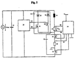
Fig. 5 zeigt einen von einem Netz mit einer Eingangswechselspannung
Uein mit einer Netzfrequenz fNetz (50 Hz) betriebenen
Verbraucher 10. Weiterhin ist ein Tiefpaßfilter 12 in Form
eines Kondensators zu dem Netz parallel und eine Spule 14 zu
dem Verbraucher 10 in Reihe angeschlossen. Die an dem Verbraucher
10 anliegende Spannung ULast laßt sich durch die erfindungsgemäße
Schaltung stufenlos im Bereich von 0 bis 100% der
Eingangswechselspannung Uein variieren. Die Schaltung umfaßt
einen ersten Wechselstromschalter 16, einen zweiten, mit einer
gegenüber der Netzfrequenz fNetz höheren Schaltfreqenz ansteuerbaren
Wechselstromschalter 32, eine Ansteuer- und Synchronisiereinrichtung
26 und eine Regeleinrichtung 34 zur Regelung
der an dem Verbraucher 10 anliegenden Wechselspannung ULast. Fig. 5 shows one of a network with an AC input voltage U a f with a line frequency AC (50 Hz) operated
Der erste Wechselstromschalter 16 umfaßt zwei ansteuerbare,
jeweils zu dem Verbraucher 10 und der Spule 14 parallel angeschlossene
Halbleiterschalter 18 und 20, die als Schutz gegenüber
Umkehrspannungen jeweils durch eine in Reihe angeschlossene
Diode 22 bzw. 24 ergänzt sind, wobei die Hableiterschalter-Diode-Kombinationen
18 und 22 bzw. 20 und 24 zueinander
antiparallel angeordnet sind. Über den zweiten
Wechselstromschalter 32 wird die Schaltung in beiden
Stromrichtungen an der Wechselspannung des Netzes betrieben.
Die Ansteuer- und Synchronisiereinrichtung 26 dient zur
Ansteuerung und zur zu der Polarität der Eingangsspannung Uein
synchronen Umschaltung der in zueinander entgegengesetzten
Schaltzuständen befindlichen Halbleiterschalter 18 und 20, ist
zur Erfassung der Polarität der Eingangsspannungs Uein
netzseitig parallel zur Eingangsspannung Uein angeschlossen und
weist zwei Ansteuerleitungen 28, 30 auf, die jeweils mit einem
der Halbleiterschalter 18 und 20 zur Ansteuerung derselben
verbunden sind.The
Der zweite Wechselstromschalter 32 ist zu dem Verbraucher 10
in Reihe angeschlossen. Über den zweiten Wechselstromschalter
32 wird die Spule 14 in beiden Stromrichtungen aufmagnetisiert.
Je nach Polarität der Eingangswechselspannung Uein wird
der entsprechende Halbleiterschalter 18 bzw. 20 aktiviert,
damit die Spule 14 bei ausgeschaltetem zweiten Wechselstromschalter
32 über den Verbraucher 10 abmagnetisieren kann. Der
Halbleiterschalter 18 wird während der negativen Netzhalbwelle
eingeschaltet (siehe auch Fig. 6), der Halbleiterschalter 20
während der positiven Netzhalbwelle (siehe auch Fig. 6). Das
bedeutet, daß die Halbleiterschalter 18 und 20 exakt synchron
zur Polarität der Eingangewechselspannung Uein umgeschaltet
werden.The
Die Regeleinrichtung 34 umfaßt einen Spannungserfassungsteil
zur Erfassung der an dem Verbraucher 10 anliegenden Ist-Wechselspannung
ULast,ist , der über zwei Leitungen 36, 38 parallel
zu dem Verbraucher 10 angeschlossen ist, einen Spannungssollwerteingabeteil
zur Eingabe des Sollwerts der an den Verbraucher
10 anliegenden Wechselspannung ULast, soll und einen Ansteuerteil,
der den zweiten Wechselstromschalter 32 mit einem zur
Erzeugung der Soll-Wechselspannung ULast, soll geeigneten Schaltfrequenz
und einem geeigneten Tastverhältnis τ (Einschaltdauer/Periodendauer)
ein- und ausschaltet. Dazu wird das Tastverhältnis
τ bei konstanter Schaltfrequenz variiert.The
Mittels eines Shunt 40 oder eines geeigneten Stromwandlers
wird der Strom durch den zweiten Wechselstromschalter 32 erfaßt
und proportional der Regeleinrichtung 34 über die Leitung
39 zugeführt.Using a
In einem stationären Arbeitspunkt, bei dem die Wechselspannung
an dem Verbraucher 0 < ULast < Uein beträgt, wird der zweite
Wechselstromschalter 32 mit einer festen Schaltfrequenz an- und
ausgeschaltet. Für einen Anstieg der Spannung ULast wird das
Tastverhältnis τ (Einschaltdauer/Periodendauer) vergrößert,
bis bei einer maximalen Spannung von ULast = Uein der zweite Wechselstromschalter
32 permanent eingeschaltet bleibt. Um die
Spannung ULast abzusenken, wird das Tastverhältnis τ bis zu dem
wert 0 verkleinert, bei dem die Spannung ULast = 0 ist (zweiter
Wechselstromschalter 32 ausgeschaltet). Die Schaltfrequenz für
den zweiten Wechelstromschalter 32 braucht nicht an die Netzfrequenz
fNetz gekoppelt zu werden und liegt im vorliegenden
Beispiel im Bereich zwischen 50 - 100 kHz. Der parallel
geschaltete Kondensator 12 dient dazu, trotz der Abtastung des
Netzstromes mit der Schaltfrequenz des zweiten Wechselstromschalters
32 einen kontinuierlich fließenden Eingangsstrom zu
erreichen.In a stationary operating point at which the AC voltage on the consumer 0 <U Last <U is one, the
Die Synchronisierung der Ansteuersignale für die Halbleiterschalter
18 und 20 zur Netzfrequenz fNetz ist von entscheidender
Bedeutung. Bei Überlappung der Ansteuersignale oder einer Phasenverschiebung
zur Netzfrequenz fNetz entstehen Kurzschlußpfade.
Bei verzögerter Aktivierung der Freilaufpfade oder Netzausfällen
(worst case im Spannungsmaximum) kann die Spule 14
nicht kontrolliert abmagnetisieren und wurden undefinierte
Spannungsspitzen entstehen.The synchronization of the control signals for the semiconductor switches 18 and 20 to the network frequency f network is of crucial importance. If the control signals overlap or a phase shift to the mains frequency f mains , short-circuit paths are created. In the event of delayed activation of the freewheeling paths or power failures (worst case in the voltage maximum), the
Die Regeleinrichtung 34 erfaßt die Spannung ULast an dem Verbraucher,
vergleicht den Wert mit dem Sollwert ULast, soll und
stellt entsprechend der Differenz ein entsprechendes Tastverhältnis
τ für den zweiten Wechselstromschalter 32 ein. Um eine
Stromüberwachung herzustellen, die bei Bedarf in die Regelung
eingreift, wird die stromproportionale Spannung am Shunt 40
erfaßt und der Regelung zugeführt. Der Bezugspunkt (Ground)
des Stromerfassungsteils liegt an der Source 42 des zweiten
Wechselstromschalters 32.The
Als Halbleiter 18, 20, 33, 35 dienen MOSFET-Transistoren. Es
kann jedoch auch jede andere Art von Transistoren, wie z.B.
Bipolartransistoren oder IGBT, etc. verwendet werden.MOSFET transistors serve as
In Fig. 6 sind die Ansteuersignale für die Halbleiterschalter
18, 20 und den zweiten Wechselstromschalter 32 sowie die zugehörigen
Ströme in Abhängigkeit von der Zeit t dem zeitlichen
Verlauf der Eingangsspannung Uein gegenübergestellt. Die
Schaltfrequenz für den zweiten Wechselstromschalter 32 ist
bewußt sehr klein gewählt, um die Signalverläufe besser darstellen
zu können. Die Ansteuersignale zeigen einen stationären
Arbeitspunkt, bei dem 0 < ULast < Uein beträgt. Der zweite
Wechselstromschalter 32 wird mit einer festen Schaltfrequenz
(Schaltzustände EIN, AUS) angesteuert. Über den zweiten Wechselstromschalter
32 fließt entsprechend der Eingangswechselspannung
Uein und der Schaltfrequenz ein pulsförmiger Strom
ISchalter 32, der der Sinusform der Eingangswechselspannung Uein
folgt. Der Strom ISpule in der Spule 14 verläuft dagegen bedingt
durch die Auf- und Abmagnetisierung, unterlagert von der Sinuskurve
der Eingangswechselspannung Uein, dreieckförmig. Der
Strom durch die Spule 14 bildet sich an dem Verbraucher mit
Ohmscher Charakteristik ohne weitere Verformung als Spannung
ULast ab. Das bedeutet, daß auch dem Verbraucher 10 eine sinusförmige
Spannung zur Verfügung steht. Mit zunehmender Schaltfrequenz
des zweiten Wechselstromschalters 32 wird die Restwelligkeit
in dem Spulenstrom ISpule, die der Sinuskurve überlagert
ist, kleiner und die Sinusform wird sehr gut erreicht.
Durch zusätzliche Befilterung von Ein- und Ausgangsstrom (s.
Tiefpaßfilter 12, 13 in Fig. 9) erreichen beide Ströme und damit
auch die Spannungen einen sinusförmigen Verlauf.In FIG. 6, the control signals for the semiconductor switches 18, 20 and the
Die an dem Verbraucher 10 anliegende Wechselspannung ULast kann
über das Tastverhältnis τ des zweiten Wechselstromschalters 32
direkt proportional eingestellt werden. Dabei fließt kontinuierlich
Strom. Bei einem Verbraucher mit Ohmscher Charakteristik
bildet sich die sinusförmige Eingangswechselspannung Uein
ohne Phasenverschiebung oder zusätzliche nichtlineare Verzerrungen
mit gleicher Frequenz wieder sinusförmig an dem Verbraucher
ab (Power-Factor = 1;
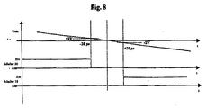
Fig. 7 zeigt eine mögliche Ausführungsform einer Stromquelle-Optokoppler-Kombination der erfindungsgemäßen Schaltung. Ein Ansteuer-Optokoppler 44 bzw. 46 dient zur Ankopplung des Ansteuersignals der Ansteuer- und Synchronisiereinrichtung 26 (s. Fig. 5). Die notwendige Ansteuerspannung wird über eine Stromquelle 48 bzw. 50 erzeugt. Mit den Ansteuer-Optokopplern 44 bzw. 46 lassen sich sehr einfach die vorhandenen Potentialunterschiede überbrücken. Die Stromquellen 48 bzw. 50 führen bereits nur sehr kurz nach dem Netznulldurchgang den für die Ansteuer-Optokoppler 44 bzw. 46 erforderlichen Strom und machen damit eine sehr exakte und schnelle Erkennung des Netzstromnulldurchgangs möglich. Ausgangsseitig steuern die Ansteuer-Optokoppler 44 bzw. 46 den ersten Wechselstromschalter, entweder direkt oder indirekt, über geeignete Treiber- oder Übertragungsstufen an. Die Stromquelle-Optokoppler-Kombination(en) ist/sind direkt an der Eingangsspannung angeschlossen. Wenn Depletion MOSFET-Transistoren verwendet werden, sind die Vorteile besonders groß. Depletion Transistoren besitzen einen passiv leitenden Kanal, wodurch bereits bei äußerst minimaler Spannung der für die Ansteuer-Optokoppler 44, 46 notwendige Strom fließen kann. Damit wird der Netzstromnulldurchgang bzw. die Netzspannungspolarität sehr exakt erfaßt. Der Bauteileaufwand für die Erzeugung der Umschaltsignale reduziert sich bei Verwendung von Depletion Transistoren auf den Transistor mit einem Widerstand in Kombination als Stromquelle, eine Schutzdiode gegen Inversspannungen und den Ansteuer-Optokoppler zur Übertragung der Signale. Damit ist diese Lösung sehr genau, äußerst billig durch den geringen Aufwand an Bauteilen und Leiterplattenflache, störunempfindlich durch den kompakten Aufbau, braucht keine zusätzliche Logik zur Auswertung, benötigt keinerlei Hilfsspannung und verbraucht nur extrem wenig Energie. Durch die sehr genaue Erkennung der Netzpolarität, wobei die Schaltung bis ca. 2 Volt Netzspannung arbeitet, ergibt sich ein weiterer besonderer Vorteil. Bei Ausfall der Netzspannung im Spannungsmaximum würden exzessive, undefinierte Induktionsspannungen an der Spule entstehen, wenn die Freilaufzweige zu früh abschalten und den Freilaufpfad sperren. Dadurch würden die Halbleiterschalter extrem gefährdet. Weil aber die Stromquelle-Optokoppler-Kombinationen bis zu einer Spannung von nur noch ca. 2 Volt sicher arbeiten, bleiben die Freilaufzweige auf jeden Fall sicher leitend und gewährleisten ein sicheres Abmagnetisieren der Spule auch bei plötzlichen Spannungsausfällen. Eine Schutzbeschaltung der Spule durch Varistoren, Kondensatoren oder ähnliches ist damit nicht notwendig. Die ganze Schaltung zur Erzeugung der Umschaltsignale reduziert sich auf einen 2-Pol, der denkbar einfach zu handhaben ist. Alternativ kann aber auch vorgesehen sein, die Synchronisiersignale durch Übertrager oder integrierte Schaltkreise, die entsprechende Potentialdifferenzen zulassen, zu übertragen. Fur die Erzeugung und Übertragung dieser Synchronsignale sind auch andere Methoden denkbar.7 shows a possible embodiment of a current source / optocoupler combination the circuit according to the invention. A Control optocouplers 44 and 46 are used to couple the control signal the control and synchronization device 26 (see Fig. 5). The necessary control voltage is via a Current source 48 and 50 generated. With the control optocouplers 44 and 46, the existing potential differences can be very easily bridge. The current sources 48 and 50 lead already very shortly after the net zero crossing for the Control optocouplers 44 and 46 required current and make thus a very exact and quick detection of the mains zero crossing possible. The control optocouplers control the output side 44 and 46 the first AC switch, either directly or indirectly, via suitable driver or Transmission levels. The power source-optocoupler combination (s) is / are directly connected to the input voltage. When using depletion MOSFET transistors the advantages are particularly great. Have depletion transistors a passively conductive channel, making it extremely minimal Voltage necessary for the control optocouplers 44, 46 Electricity can flow. This will make the mains current zero crossing or the mains voltage polarity is recorded very precisely. Of the Component effort for generating the switchover signals reduced when using depletion transistors Transistor with a resistor in combination as a current source, a protective diode against inverse voltages and the control optocoupler for the transmission of the signals. So this is the solution very accurate, extremely cheap due to the low effort Components and PCB area, insensitive to interference from the compact structure, does not need any additional logic for evaluation, does not require any auxiliary voltage and only consumes extremely little energy. Due to the very precise detection of the network polarity, the circuit up to about 2 volts mains voltage works, there is another particular advantage. At Failure of the mains voltage at the maximum voltage would be excessive, undefined induction voltages on the coil arise when turn off the freewheel branches too soon and the freewheel path lock. This would extremely endanger the semiconductor switches. But because the power source-optocoupler combinations up to work safely to a voltage of only about 2 volts, the freewheel branches definitely remain conductive and ensure a safe demagnetization of the coil sudden power failures. A protective circuit of the Coil through varistors, capacitors or the like is so unnecessary. The whole circuit for generating the switching signals is reduced to a 2-pole, which is very simple is to be handled. Alternatively, it can also be provided be the synchronizing signals by transformers or integrated Circuits, the corresponding potential differences allow to transfer. For generation and transmission other methods are also conceivable for these synchronous signals.
Es steht somit für mindestens eine Netzhalbwelle eine Stromquelle
48,50 zur Verfügung, die den jeweiligen Ansteuer-Optokoppler
44,46 des entsprechenden Freilaufpfads ansteuert. Diese
Stromquellen-Optokoppler-Kombinationen sind direkt an der
Netzspannung angeordnet. Um den Nulldurchgang der Netzspannung
möglichst genau als Umschaltpunkt für die Freilaufpfade zu
finden und nur eine minimale Totzeit zwischen beiden Steuersignalen
für die Gleichstromschalter 18, 20 zu erreichen, werden
Stromquellen 48,50 eingesetzt, die bereits bei extrem geringer
Netzspannung, d.h. nur kurz nach dem Spannungsnulldurchgang`
den für die Ansteuer-Optokoppler 44,46 notwendigen Strom führen.
Mit den Stromquellen 48 (negative Netzhalbwelle) und 50
(positive Netzhalbwelle), die jeweils einen Depletion MOSFET-Transistor
umfassen, können hervorragende Werte erreicht werden.
Da der Depletion Transistor einen passiv leitenden Kanal
besitzt, genügt die Schwellspannung der Ansteuer-Optokopplerdiode
und der Schutzdiode 42 bzw. 43, um die Steuerung zu aktivieren.
Die Totzeit im Spannungsnulldurchgang beträgt mit
dieser Anordnung bei einem 230 Volt rms/50 Hz-Netz nur ca. ±20
µs (siehe Fig. 7 und 8). Das bedeutet, daß bei einer Momentanspannung
von nur 2 Volt die beiden Freilaufpfade umgeschaltet
werden. Mit derart kleinen Spannungswerten bleibt die Energie
in der Spule 14 so gering, daß für die Schaltung keine Gefahr
besteht. Mit dieser Konfiguration der Ansteueranordnung wird
die Schlüsselfunktion der Schaltung ideal gelöst.A current source therefore stands for at least one network half-wave
48.50 available, the respective control optocoupler
44.46 of the corresponding freewheeling path. This
Power source-optocoupler combinations are directly on the
Mains voltage arranged. Around the zero crossing of the mains voltage
as accurate as possible as a switchover point for the freewheel paths
find and only a minimal dead time between the two control signals
for the DC switches 18, 20 to be reached
Power sources 48.50 used that are already extremely low
Mains voltage, i.e. only shortly after the voltage zero crossing`
carry the current required for the control optocouplers 44, 46.
With the current sources 48 (negative mains half-wave) and 50
(positive line half-wave), each with a depletion MOSFET transistor
excellent values can be achieved.
Because the depletion transistor has a passively conductive channel
the threshold voltage of the drive optocoupler diode is sufficient
and the protection diode 42 and 43 to activate the control.
The dead time in the zero voltage crossing is with
this arrangement for a 230 volt rms / 50 Hz network only approx. ± 20
µs (see Fig. 7 and 8). That means that at a momentary tension
the two freewheeling paths can be switched from just 2 volts
will. With such small voltage values, the energy remains
in the
Fig. 9 zeigt ein weiter konkretisiertes und teilweise abgeändertes
Beispiel für die in Fig. 5 gezeigte Schaltung. Die Konkretisierung
bezieht sich im wesentlichen auf die Ansteuer- und
Synchronisiereinrichtung (Netzsynchronisierung). Der in
Fig. 9 gezeigte zweite Wechselstromschalter 32 umfaßt zwei
Halbleiterschalter 33, 35 in Form von zwei gegensinnig in Reihe
geschalteten MOSFET-Transistoren. Um höhere Leistungen zu
erreichen, können optional weitere Transistoren (im Beispiel
IGBTs) parallel geschaltet werden. Die Transistoren sind am
Gate über Vorwiderstände direkt parallel geschaltet und werden
alle mit dem gleichen Ansteuersignal betrieben.9 shows a more specific and partially modified one
Example of the circuit shown in FIG. 5. The concretization
essentially refers to the control and
Synchronization device (network synchronization). The in
9,
Entsprechend der Polarität der Eingangsspannung wird die zulässige
Stromrichtung im ersten Wechselstromschalter 16 umgeschaltet.
Während der positiven Netzhalbwelle wird der Halbleiterschalter
20 eingeschaltet und leitet der Halbleiterschalter
18 über die integrierte Inversdiode den Freilaufstrom.
Während der negativen Netzhalbwelle bleibt der Halbleiterschalter
18 eingeschaltet (Halbleiterschalter 20 ausgeschaltet)
und leitet der Halbleiterschalter 20 über die Inversdiode
den Freilaufstrom. Die Ansteuersignale kommen über
die Stromquellen-Optokoppler-Kombination 26 und werden durch
die Optokoppler 44, 46 und die nachfolgenden Treiber (Transistoren
oder integrierte Treiber oder ähnliches) an die Halbleiterschalter
18, 20 übertragen. Die notwendige Hilfsspannung
wird von einem über Kondensatoren am Netz angeschlossenen
Gleichrichter mit einer nachgeschalteten Stromquelle erzeugt.According to the polarity of the input voltage, the permissible
Current direction switched in the
Zur Regelung der an dem Verbraucher anliegenden Spannung ULast wird mit einem Differenzverstärker die Ist-Spannung ULast, ist an dem Verbraucher proportional erfaßt und geeignet aufbereitet. To regulate the voltage U load applied to the consumer, the actual voltage U load is detected with a differential amplifier and is proportionally acquired at the consumer and suitably processed.
Ein nachfolgender Regler vergleicht den Ist-Spannungswert ULast,
ist mit einem geforderten Sollwert ULast, soll und gibt die Abweichung
an einen Schaltregler weiter. Zur Strombegrenzung wird
die Spannung am Shunt-Widerstand 40 erfaßt, aufbereitet und
proportional an den Schaltregler weitergegeben. Bei Überschreiten
eines bestimmten Schwellwerts reduziert der Schaltregler
das Tastverhältnis` Im vorliegenden Ausführungsbeispiel
ist sowohl am Eingang als auch am Ausgang ein Tiefpaßfilter
12, 13 vorgesehen. Die Tiefpaßfilter 12, 13 an den Ein- und
Ausgängen sind in diesem Beispiel aufwendiger als in den anderen
Figuren ausgeführt, in denen nur ein Kondensator dargestellt
ist. Es sind Jedoch auch andere Varianten der Ausführungsformen
der Tiefpaßfilter 12, 13 denkbar.A subsequent controller compares the actual voltage value U load, is with a required setpoint U load, and transmits the deviation to a switching controller. To limit the current, the voltage at the
Fig. 10 zeigt schematisch eine weitere Ausführungsform der erfindungsgemäßen
Schaltung, die eine Regeleinrichtung 34 für
den Strom und einen ersten Wechselstromschalter 16 mit zwei
Halbleiterschaltern 18, 20 in Form von zwei in Reihe geschalteten
IGBTs mit gemeinsam verbundener Kollektor-Elektrode umfaßt.
Der Sollwert für den Ausgangsstrom wird in diesem Beispiel
potentialgetrennt über Optokoppler übertragen. Eine
Stromregelung kann insbesondere bei stark nichtlinearen Verbrauchertypen
gegenüber einer Spannungsregelung deutliche Vorteile
bieten, da für die Einhaltung der Normen EN61000-3-2,
EN61000-3-3 und EN61000-3-4 die Ströme von entscheidender Bedeutung
sind. Im folgenden soll im wesentlichen nur auf die
Unterschiede zu den in Fig. 5 und 9 gezeigten Ausführungsformen
eingegangen werden. Bei dieser Ausführungsform wird nicht
der Sollwert der an einem Verbraucher 10 anliegenden Spannung
ULast, soll sondern der Sollwert für den durch den Verbraucher 10
fließenden Strom ILast, soll über einen Eingabeteil der Regeleinrichtung
34 vorgegeben. Der Ist-Gleich- und/oder -Wechselstromwert
des durch den Verbraucher 10 fließenden Stroms ILast,
ist wird über die Leitung 36 und einen geeigneten Stromwandler
52 erfaßt. Ein Ansteuerteil der Regeleinrichtung 34 steuert
dann den zweiten Wechselstromschalter 32 mit einem zur Erzeugung
des Sollstroms geeigneten Tastverhä ltnis τ bei einer
konstanten Schaltfrequenz an. Die Stromerfassung mit einem
Shunt 40 kann weiterhin als Spitzenstrombegrenzung und Kurzschlußschutz
verwendet werden.10 schematically shows a further embodiment of the circuit according to the invention, which comprises a
Fig. 11 zeigt eine Variante zu Fig. 10, in der die Halbleiterschalter
18 und 20 des ersten Wechselstromschalters 16 über
ein einziges Ansteuersignal 30 der Ansteuer- und Synchronisiereinrichtung
26, das über eine Stromquelle-Optokoppler-Kombination
über eine Ansteuerleitung 30 direkt den Halbleiterschalter
20 und über eine Invertiereinrichtung 54 und eine
Ansteuerleitung 28 den Halbleiterschalter 18 invers zu dem
Halbleiterschalter 20 ansteuert. Durch diese Art der Ansteuerung
wird eine zweite Stromquelle-Optokoppler-Kombination gespart
sowie keine zweite Ansteuersignalerzeugung notwendig. Im
einzelnen sieht die Schaltung wie folgt aus: Der erste Wechselstromschalter
16 weist zwei Halbleiterschalter 18, 20 in
Form von zwei IGBTs mit Inversdiode auf, die über die Emitter
miteinander verbunden sind, so daß ein gemeinsamer Steuerground
vorliegt. Die Ansteuer- und Synchronisiereinrichtung 26
weist nur eine Stromquelle-Optokoppler-Kombination und nur
eine Steuerleitung 30 zum ersten Wechselstromschalter 16 auf.
Die andere Steuerleitung 28 wird mittels eines Inverters 54
(Transistor, Operationsverstärker oder integrierter Inverter)
erzeugt. Der zweite Wechselstromschalter 32 besteht aus zwei
MOSFET in Reihe mit gemeinsamen Source-Potential, denen je ein
IGBT parallelgeschaltet ist, was zu einer Leistungserhöhung
führt. Der Strom zu dem zweiten Wechselstromschalter 32 wird
mit einem Stromwandler 52 erfaßt und über die Leitung 39 der
Regeleinrichtung 34 zugeführt. Dadurch wird eine Strombegrenzung
und ein Kurzschlußschutz erzielt. Der Verbraucher 10 ist
ein Transformator (, wodurch keine separate Induktivität notwendig
ist,), der einen nichtlinearen Heizwiderstand versorgt.
Die Temperatur dieser Heizung wird über einen Temperatursensor
41 und Leitung 36 der Regeleinrichtung 34 zugeführt. Als Sollwert
erhält die Regeleinrichtung 34 über eine Potentialtrennung
den Temperatursollwert und stellt entsprechend der Abweichung
zwischen Ist-Wert und Soll-Wert das Tastverhältnis an
dem zweiten Wechselstromschalter 32 ein. Das heißt, daß der
Laststrom indirekt über die Temperatur eingestellt wird. Bei
anderen Verbrauchertypen würden andere Größen erfaßt bzw. der
Regeleinrichtung als Sollwert vorgegeben. Zum Beispiel bei
einem Motor würde die Drehzahl oder das Drehmoment erfaßt bzw.
als Sollwert vorgegeben. Entsprechend dem Verbraucher werden
die erforderlichen Größen der Regeleinrichtung 34 zugeführt
bzw. als Sollwert vorgegeben.Fig. 11 shows a variant of Fig. 10, in which the
Fig. 12 zeigt schematisch eine weitere Ausführungsform der
erfindungsgemäßen Schaltung, die eine Stromregeleinrichtung
und einen ersten und zweiten Wechselstromschalter umfaßt, die
invers zueinander und nicht netzsynchron angesteuert werden.
Der erste Wechselstromschalter 16 ist wie der erste Wechselstromschalter
16 in Fig. 11 gestaltet. Der zweite Wechselstromschalter
32 weist wiederum zwei Halbleiterschalter 33 und
35 und einen Stromwandler als Überlastschutz auf. Über eine
Invertiereinrichtung 54 werden die ersten und zweiten Wechselstromschalter
16 und 32 invers zueinander und nicht netzsynchron
angesteuert.12 schematically shows a further embodiment of the
Circuit according to the invention, which is a current control device
and comprises first and second AC switches, the
inverse to each other and not synchronized to the network.
The
Fig. 13 zeigt die Ansteuersignale und Strom- und Spannungsverläufe
bei einer besonderen Betriebsform der in Fig. 12 gezeigten
Schaltung. Es erübrigt sich eine Netzsynchronisierung.
Während der zweite Wechselstromschalter 32 eingeschaltet ist
(Aufmagnetisierung der Spule 14), bleibt der erste Wechselstromschalter
16 ausgeschaltet, um keinen Kurzschlußpfad zu
bilden. Wenn der zweite Wechselstromschalter 32 ausgeschaltet
wird, muß der erste Wechselstromschalter 16 eingeschaltet werden,
um für beide Stromrichtungen die Abmagnetisierung der
Spule 14 zu gewahrleisten. Die beiden ersten und zweiten Wechselstromschalter
16 und 32 werden somit invers zueinander ein- bzw.
ausgeschaltet.13 shows the control signals and current and voltage profiles
in a particular mode of operation that shown in FIG
Circuit. There is no need for network synchronization.
While the
Die erfindungsgemäße Schaltung erfüllt die Anforderungen der oben erläuterten Normen EN61000-3-2, EN61000-3-3 und EN61000-3-4 und weist minimale Verluste, einen maximalen Wirkungsgrad, keinen Blindstrom, keine Phasendrift, keine Nichtlinearität, kontinuierlichen Stromfluß ohne periodische oder aperiodische Unterbrechungen in allen Lastpunkten und einen Regelbereich von 0 bis 100% der Eingangsspannung Uein auf. Wird zwischen zwei Arbeitspunkten, z.B. durch eine Sprungfunktion, gewechselt, so ist eine Anpassung der Spannungssollwertvorgabe an den verwendeten Verbrauchertyp (z.B. trapezförmige Sollwertvorgabe) sinnvoll. Bei einer digitalen Sollwertvorgabe durch einen Mikroprozessor können derartige verbrauchertypische Daten einmal ermittelt und je nach Konfiguration der Endanwendung z.B. in ROM-Speichern abgelegt werden. Es gilt also herauszufinden, mit welcher maximalen Schaltdynamik (Änderungsgeschwindigkeit von Sollwerten) der Verbraucher betrieben werden kann, damit die Konformität zur Norm EN61000-3-3 nicht verletzt wird. Die Einschränkung zur Einhaltung dieser Norm wird nicht mehr von der Schaltung (vorgeschalteter Wandler) bestimmt, sondern liegt nun einzig und allein beim eingesetzten Verbrauchertyp, den es zu charakterisieren gilt. Liegen diese Daten fest, die die theoretisch maximale Sollwertdynamik beschreiben, kann der Verbraucher auch tatsächlich mit dieser Grenzdynamik ideal betrieben werden.The circuit according to the invention meets the requirements of the standards EN61000-3-2, EN61000-3-3 and EN61000-3-4 explained above and has minimal losses, maximum efficiency, no reactive current, no phase drift, no non-linearity, continuous current flow without periodic or aperiodic interruptions in all load points and a control range of 0 to 100% of the input voltage U in. If you switch between two operating points, e.g. using a step function, it is advisable to adapt the voltage setpoint specification to the consumer type used (eg trapezoidal setpoint specification). With a digital setpoint specification by a microprocessor, such consumer-specific data can be determined once and, depending on the configuration of the end application, can be stored, for example, in ROM memories. It is therefore important to find out with which maximum switching dynamics (rate of change of setpoints) the consumer can be operated so that the conformity to the standard EN61000-3-3 is not violated. The restriction to comply with this standard is no longer determined by the circuit (upstream converter), but now lies solely with the type of consumer used, which must be characterized. Once these data are available that describe the theoretical maximum setpoint dynamics, the consumer can actually be operated ideally with this limit dynamics.
Die Form, Amplitude und Frequenz der Netzspannung können beliebig sein. Vorzugsweise wird die erfindungsgemäße Schaltung an den international üblichen Gleich- und/oder Wechselspannungsnetzen betrieben, und zwar mit z.B. fNetz ≥ O Hz und sinusförmigem Strom- und Spannungsverlauf. The shape, amplitude and frequency of the mains voltage can be any. The circuit according to the invention is preferably operated on the internationally customary direct and / or alternating voltage networks , specifically with eg f network O O Hz and sinusoidal current and voltage curve.
Die in der vorangehenden Beschreibung, in der Zeichnung sowie in den Ansprüchen offenbarten Merkmale der Erfindung können sowohl einzeln als auch in beliebigen Kombinationen für die Verwirklichung der Erfindung in ihren verschiedenen Ausführungsformen wesentlich sein. The in the previous description, in the drawing as well features of the invention disclosed in the claims both individually and in any combination for the Realization of the invention in its various embodiments be essential.
- 1010th
- Verbraucherconsumer
- 1212th
- Tiefpaßfilter EingangLow pass filter input
- 1313
- Tiefpaßfilter AusgangLow pass filter output
- 1414
- SpuleKitchen sink
- 1616
- erster Wechselstromschalterfirst AC switch
- 18, 2018, 20
- HalbleiterschalterSemiconductor switch
- 22, 2422, 24
- Diodediode
- 2626
- Ansteuer- und SynchronisiereinrichtungControl and synchronization device
- 28, 3028, 30
- AnsteuerleitungControl line
- 3232
- zweiter Wechselstromschaltersecond AC switch
- 3333
- HalbleiterschalterSemiconductor switch
- 3434
- RegeleinrichtungControl device
- 3535
- HalbleiterschalterSemiconductor switch
- 36, 38, 3936, 38, 39
- Leitungmanagement
- 4040
- ShuntShunt
- 4141
- TemperatursensorTemperature sensor
- 42, 4342, 43
- Diodediode
- 44, 4644, 46
- Ansteuer-OptokopplerControl optocoupler
- 44a, 44b44a, 44b
- Ansteuer-OptokopplerControl optocoupler
- 46a, 46b46a, 46b
- Ansteuer-OptokopplerControl optocoupler
- 48, 5048, 50
- StromquellePower source
- 5252
- StromwandlerPower converter
- 5454
- InvertiereinrichtungInverting device
Claims (15)
gekennzeichnet durch
marked by
Applications Claiming Priority (4)
| Application Number | Priority Date | Filing Date | Title |
|---|---|---|---|
| DE19710161A DE19710161C2 (en) | 1997-03-12 | 1997-03-12 | Circuit for continuously variable direct or indirect variation of the direct current and / or alternating current flowing through a consumer operated by a mains direct or alternating voltage or any combination thereof |
| DE19710161 | 1997-03-12 | ||
| DE1997141655 DE19741655A1 (en) | 1997-03-12 | 1997-09-22 | Circuit for continuously variable direct or indirect variation of the direct current and / or alternating current flowing through a consumer operated by a direct or alternating voltage or any combination thereof |
| DE19741655 | 1997-09-22 |
Publications (2)
| Publication Number | Publication Date |
|---|---|
| EP0865150A2 true EP0865150A2 (en) | 1998-09-16 |
| EP0865150A3 EP0865150A3 (en) | 1999-12-01 |
Family
ID=26034768
Family Applications (1)
| Application Number | Title | Priority Date | Filing Date |
|---|---|---|---|
| EP19980104518 Withdrawn EP0865150A3 (en) | 1997-03-12 | 1998-03-12 | Circuit for continuous direct or indirect variation of DC and/or AC current flowing in a load supplied by DC or AC source voltage or any combination of these voltages |
Country Status (3)
| Country | Link |
|---|---|
| US (1) | US5932934A (en) |
| EP (1) | EP0865150A3 (en) |
| DE (1) | DE19741655A1 (en) |
Cited By (8)
| Publication number | Priority date | Publication date | Assignee | Title |
|---|---|---|---|---|
| WO2000042700A1 (en) * | 1999-01-14 | 2000-07-20 | Dip Digital Power Systems Ag | Bipolar chopper and method of using same |
| EP1137158A1 (en) * | 2000-03-21 | 2001-09-26 | Kabushiki Kaisha Toshiba | AC switch device used for switching AC circuit and AC switch circuit having the AC switch device |
| DE10160361A1 (en) * | 2001-12-08 | 2003-07-03 | Ixys Semiconductor Gmbh | Device for providing alternating or 3-phase currents has control circuit that switches reverse blocking IGBTs connected in reverse parallel on and off during positive and negative half waves |
| US6727891B2 (en) | 2001-07-03 | 2004-04-27 | Netmor, Ltd. | Input device for personal digital assistants |
| DE102005032085A1 (en) * | 2005-07-08 | 2007-01-18 | Siemens Ag | Device for reducing the power during the operation of an inductive load |
| DE102006029502A1 (en) * | 2006-06-27 | 2008-01-03 | Lite Puter Enterprise Co., Ltd., Sijhih | Sine wave light-adjusting apparatus for lamp, has negative semi-period flywheel unit, connected with energy-storing unit and lighting unit, which is controlled by microprocessor to conduct during negative semi-period of sine wave voltage |
| DE102010024128A1 (en) * | 2010-06-17 | 2011-12-22 | Diehl Ako Stiftung & Co. Kg | Alternating voltage regulators |
| DE102018203487A1 (en) * | 2018-03-08 | 2019-09-12 | Continental Automotive Gmbh | Vehicle electrical system |
Families Citing this family (20)
| Publication number | Priority date | Publication date | Assignee | Title |
|---|---|---|---|---|
| FR2802730A1 (en) * | 1999-12-17 | 2001-06-22 | Crouzet Automatismes | METHOD FOR CONTROLLING AN ELECTRIC ENERGY CONVERTER OF THE ALTERNATIVE-ALTERNATIVE TYPE AND CONTROL DEVICE FOR IMPLEMENTING THE METHOD |
| US6559619B1 (en) * | 2000-07-25 | 2003-05-06 | Daniel G. Bach | Energy management controller |
| ITRM20020124A1 (en) * | 2002-03-06 | 2003-09-08 | Sisti Lighting S P A De | ELECTRONIC DEVICE FOR ADJUSTING THE POWER SUPPLY APPLIED TO A LOAD, OR DIMMER. |
| ES2201937B1 (en) | 2003-11-03 | 2005-02-01 | Bsh Electrodomesticos España, S.A. | PROCEDURE FOR THE OPERATION OF A CONVERTER CIRCUIT. |
| US20070228593A1 (en) * | 2006-04-03 | 2007-10-04 | Molecular Imprints, Inc. | Residual Layer Thickness Measurement and Correction |
| GB0526626D0 (en) * | 2005-12-30 | 2006-02-08 | Microgen Energy Ltd | A method of regulating an AC signal |
| GB0526635D0 (en) | 2005-12-30 | 2006-02-08 | Microgen Energy Ltd | Switching controller |
| GB0526625D0 (en) * | 2005-12-30 | 2006-02-08 | Microgen Energy Ltd | Power supply |
| DE102006049507B4 (en) * | 2006-10-17 | 2016-05-25 | Sew-Eurodrive Gmbh & Co Kg | Plant and method for operating a plant |
| ITVA20070038A1 (en) * | 2007-03-30 | 2008-09-30 | St Microelectronics Srl | TRANSFORMATION DEVICE FOR A PRIMARY ALTERNATE VOLTAGE IN A LOWER ALTERNATE VOLTAGE TO POWER AN ELECTRIC LOAD |
| US7688044B2 (en) * | 2007-03-30 | 2010-03-30 | Stmicroelectronics S.R.L. | Device for transforming and stabilizing a primary AC voltage for supplying an electric load |
| US7741883B2 (en) * | 2008-05-21 | 2010-06-22 | Honeywell International Inc. | Method of switching and switching device for solid state power controller applications |
| US8306448B2 (en) | 2010-07-22 | 2012-11-06 | Xerox Corporation | Fuser system and heat source power circuit |
| JP5783997B2 (en) * | 2012-12-28 | 2015-09-24 | 三菱電機株式会社 | Power semiconductor device |
| EP3198999B1 (en) * | 2014-09-23 | 2020-06-24 | Switchbee Ltd. | A method and apparatus for controlling a load |
| CN105978307B (en) * | 2016-06-13 | 2019-11-08 | 中国人民解放军海军工程大学 | EMI for PWM wave filters frequency power transformation inductive circuit |
| WO2018087374A1 (en) * | 2016-11-14 | 2018-05-17 | Abb Schweiz Ag | Switching of paralleled reverse conducting igbt and wide bandgap switch |
| TWI624132B (en) * | 2016-12-27 | 2018-05-11 | 飛宏科技股份有限公司 | Intelligent power distributing system for charging station |
| CN109036812B (en) * | 2017-06-12 | 2024-04-12 | 天津市中力神盾电子科技有限公司 | Current acquisition device |
| RU187861U1 (en) * | 2018-12-03 | 2019-03-22 | Федеральное государственное бюджетное образовательное учреждение высшего образования "Национальный исследовательский Мордовский государственный университет им. Н.П. Огарёва" | Zero Current Transition Detector |
Citations (7)
| Publication number | Priority date | Publication date | Assignee | Title |
|---|---|---|---|---|
| GB2045549A (en) * | 1979-03-06 | 1980-10-29 | Gould Advance Ltd | Power regulating apparatus |
| US4357572A (en) * | 1981-03-26 | 1982-11-02 | Bell Telephone Laboratories, Incorporated | Current flare out limit control for PWM converter |
| US4456855A (en) * | 1981-06-15 | 1984-06-26 | Oy Helvar | Intensity regulator, especially a light regulator |
| US4626768A (en) * | 1984-01-18 | 1986-12-02 | Steve Smith | High-speed feedback circuit with ungrounded load |
| EP0631372A1 (en) * | 1993-06-24 | 1994-12-28 | Strand Lighting Limited | Power control circuit |
| WO1996021894A1 (en) * | 1995-01-11 | 1996-07-18 | Microplanet Ltd. | Method and apparatus for electronic power control |
| JPH0934564A (en) * | 1995-07-18 | 1997-02-07 | Chiyoda:Kk | Input waveform follow-up type ac power unit |
Family Cites Families (3)
| Publication number | Priority date | Publication date | Assignee | Title |
|---|---|---|---|---|
| DE3509451A1 (en) * | 1985-03-15 | 1986-09-25 | Müller, Hans, Dipl.-Betriebsw. (FH), 7730 Villingen-Schwenningen | Circuit arrangement |
| DE4428682C2 (en) * | 1994-08-12 | 1997-01-23 | Robert Seuffer Gmbh & Co | Process for supplying an inductive load with sinusoidal alternating current and alternating current regulator therefor |
| US5631814A (en) * | 1995-06-16 | 1997-05-20 | Abraham Lavsky | Uninterruptible power supply based on non-invasive connection of backup circuit to switch power supply |
-
1997
- 1997-09-22 DE DE1997141655 patent/DE19741655A1/en not_active Withdrawn
-
1998
- 1998-03-12 US US09/041,816 patent/US5932934A/en not_active Expired - Lifetime
- 1998-03-12 EP EP19980104518 patent/EP0865150A3/en not_active Withdrawn
Patent Citations (7)
| Publication number | Priority date | Publication date | Assignee | Title |
|---|---|---|---|---|
| GB2045549A (en) * | 1979-03-06 | 1980-10-29 | Gould Advance Ltd | Power regulating apparatus |
| US4357572A (en) * | 1981-03-26 | 1982-11-02 | Bell Telephone Laboratories, Incorporated | Current flare out limit control for PWM converter |
| US4456855A (en) * | 1981-06-15 | 1984-06-26 | Oy Helvar | Intensity regulator, especially a light regulator |
| US4626768A (en) * | 1984-01-18 | 1986-12-02 | Steve Smith | High-speed feedback circuit with ungrounded load |
| EP0631372A1 (en) * | 1993-06-24 | 1994-12-28 | Strand Lighting Limited | Power control circuit |
| WO1996021894A1 (en) * | 1995-01-11 | 1996-07-18 | Microplanet Ltd. | Method and apparatus for electronic power control |
| JPH0934564A (en) * | 1995-07-18 | 1997-02-07 | Chiyoda:Kk | Input waveform follow-up type ac power unit |
Cited By (10)
| Publication number | Priority date | Publication date | Assignee | Title |
|---|---|---|---|---|
| WO2000042700A1 (en) * | 1999-01-14 | 2000-07-20 | Dip Digital Power Systems Ag | Bipolar chopper and method of using same |
| EP1137158A1 (en) * | 2000-03-21 | 2001-09-26 | Kabushiki Kaisha Toshiba | AC switch device used for switching AC circuit and AC switch circuit having the AC switch device |
| US6727891B2 (en) | 2001-07-03 | 2004-04-27 | Netmor, Ltd. | Input device for personal digital assistants |
| DE10160361A1 (en) * | 2001-12-08 | 2003-07-03 | Ixys Semiconductor Gmbh | Device for providing alternating or 3-phase currents has control circuit that switches reverse blocking IGBTs connected in reverse parallel on and off during positive and negative half waves |
| DE102005032085A1 (en) * | 2005-07-08 | 2007-01-18 | Siemens Ag | Device for reducing the power during the operation of an inductive load |
| US7208848B2 (en) | 2005-07-08 | 2007-04-24 | Siemens Aktiengesellschaft | Device for power reduction during the operation of an inductive load |
| DE102006029502A1 (en) * | 2006-06-27 | 2008-01-03 | Lite Puter Enterprise Co., Ltd., Sijhih | Sine wave light-adjusting apparatus for lamp, has negative semi-period flywheel unit, connected with energy-storing unit and lighting unit, which is controlled by microprocessor to conduct during negative semi-period of sine wave voltage |
| DE102010024128A1 (en) * | 2010-06-17 | 2011-12-22 | Diehl Ako Stiftung & Co. Kg | Alternating voltage regulators |
| DE102018203487A1 (en) * | 2018-03-08 | 2019-09-12 | Continental Automotive Gmbh | Vehicle electrical system |
| DE102018203487B4 (en) | 2018-03-08 | 2022-06-23 | Vitesco Technologies GmbH | vehicle electrical system |
Also Published As
| Publication number | Publication date |
|---|---|
| US5932934A (en) | 1999-08-03 |
| EP0865150A3 (en) | 1999-12-01 |
| DE19741655A1 (en) | 1999-03-25 |
Similar Documents
| Publication | Publication Date | Title |
|---|---|---|
| EP0865150A2 (en) | Circuit for continuous direct or indirect variation of DC and/or AC current flowing in a load supplied by DC or AC source voltage or any combination of these voltages | |
| EP2178201B1 (en) | Method and control system for transforming an AC voltage into a consumer supply voltage with adjustable rms value | |
| DE2461440C2 (en) | Circuit arrangement for operating a single-phase AC or DC load | |
| EP1715582B1 (en) | Circuit arrangement for driving an electric power switch at high voltage | |
| EP1073192B1 (en) | Method and device for driving an AC load, especially an AC motor with speed control | |
| AT403865B (en) | VOLTAGE CONVERSION DEVICE FOR A DC VOLTAGE CONSUMER | |
| CH698835B1 (en) | Internal power supply for converter switch driver. | |
| EP1538736A2 (en) | Drive system | |
| DE102007041510A1 (en) | Multichannel DC-DC controller | |
| DE3841147C2 (en) | ||
| EP1892811A2 (en) | Power converter circuit and method for feeding into the mains from a DC source with a non constant DC | |
| WO2014206704A1 (en) | Converter assembly having multi-step converters connected in parallel and method for controlling said multi-step converters | |
| WO2018019944A1 (en) | Drive converter for a switched reluctance machine | |
| WO2017133964A1 (en) | Improved power converter | |
| DE102014101571B4 (en) | INVERTER AND PROCESS FOR OPERATING AN INVERTER | |
| DE10245368B4 (en) | Welding power source for DC and AC welding and method of operation | |
| EP3174204B1 (en) | Method and device for controlling an electric or electronic switching element | |
| EP1126591B1 (en) | Method and device for controlling or regulating power of low ohmic heating resistors | |
| EP0751611B1 (en) | Power converter circuit | |
| DE19710161C2 (en) | Circuit for continuously variable direct or indirect variation of the direct current and / or alternating current flowing through a consumer operated by a mains direct or alternating voltage or any combination thereof | |
| CH660652A5 (en) | INVERTER ARRANGEMENT. | |
| DE1058615B (en) | Device for controlling the supply of a load from an alternating current source | |
| DE10044574A1 (en) | Variable control circuit for AC load e.g. lighting or heating device or variable speed motor, uses phase chopping of rectified sinusoidal half waves of supply network voltage | |
| DE102008034989B4 (en) | Circuit arrangement and method for controlling the power consumption of lighting systems with AC power supply | |
| AT508808B1 (en) | ONE AND TWO QUADRANTS CONTROLLERS WITH SPARTRAFO |
Legal Events
| Date | Code | Title | Description |
|---|---|---|---|
| PUAI | Public reference made under article 153(3) epc to a published international application that has entered the european phase |
Free format text: ORIGINAL CODE: 0009012 |
|
| AK | Designated contracting states |
Kind code of ref document: A2 Designated state(s): AT BE CH DE DK ES FI FR GB GR IE IT LI LU MC NL PT SE |
|
| AX | Request for extension of the european patent |
Free format text: AL;LT;LV;MK;RO;SI |
|
| PUAL | Search report despatched |
Free format text: ORIGINAL CODE: 0009013 |
|
| AK | Designated contracting states |
Kind code of ref document: A3 Designated state(s): AT BE CH DE DK ES FI FR GB GR IE IT LI LU MC NL PT SE |
|
| AX | Request for extension of the european patent |
Free format text: AL;LT;LV;MK;RO;SI |
|
| RIC1 | Information provided on ipc code assigned before grant |
Free format text: 6H 02M 5/293 A, 6H 02M 3/156 B |
|
| 17P | Request for examination filed |
Effective date: 20000530 |
|
| AKX | Designation fees paid |
Free format text: AT BE CH DE DK ES FI LI |
|
| RBV | Designated contracting states (corrected) |
Designated state(s): AT BE CH DE DK ES FI FR GB GR IE IT LI LU MC NL PT SE |
|
| RAP1 | Party data changed (applicant data changed or rights of an application transferred) |
Owner name: ASCOM ENERGY SYSTEMS GMBH |
|
| 17Q | First examination report despatched |
Effective date: 20031216 |
|
| RAP1 | Party data changed (applicant data changed or rights of an application transferred) |
Owner name: DELTA ENERGY SYSTEMS (SWITZERLAND) AG |
|
| RAP1 | Party data changed (applicant data changed or rights of an application transferred) |
Owner name: DELTA ENERGY SYSTEMS (SWITZERLAND) AG |
|
| STAA | Information on the status of an ep patent application or granted ep patent |
Free format text: STATUS: THE APPLICATION IS DEEMED TO BE WITHDRAWN |
|
| 18D | Application deemed to be withdrawn |
Effective date: 20050614 |