EP0864537A1 - Ferroelectric material, method of manufacturing the same, semiconductor memory, and method of manufacturing the same - Google Patents
Ferroelectric material, method of manufacturing the same, semiconductor memory, and method of manufacturing the same Download PDFInfo
- Publication number
- EP0864537A1 EP0864537A1 EP97941264A EP97941264A EP0864537A1 EP 0864537 A1 EP0864537 A1 EP 0864537A1 EP 97941264 A EP97941264 A EP 97941264A EP 97941264 A EP97941264 A EP 97941264A EP 0864537 A1 EP0864537 A1 EP 0864537A1
- Authority
- EP
- European Patent Office
- Prior art keywords
- film
- ferroelectric
- substrate
- target
- remno
- Prior art date
- Legal status (The legal status is an assumption and is not a legal conclusion. Google has not performed a legal analysis and makes no representation as to the accuracy of the status listed.)
- Granted
Links
Images
Classifications
-
- H—ELECTRICITY
- H10—SEMICONDUCTOR DEVICES; ELECTRIC SOLID-STATE DEVICES NOT OTHERWISE PROVIDED FOR
- H10D—INORGANIC ELECTRIC SEMICONDUCTOR DEVICES
- H10D64/00—Electrodes of devices having potential barriers
- H10D64/01—Manufacture or treatment
- H10D64/013—Manufacture or treatment of electrodes having a conductor capacitively coupled to a semiconductor by an insulator
- H10D64/01302—Manufacture or treatment of electrodes having a conductor capacitively coupled to a semiconductor by an insulator the insulator being formed after the semiconductor body, the semiconductor being silicon
- H10D64/01332—Making the insulator
- H10D64/01336—Making the insulator on single crystalline silicon, e.g. chemical oxidation using a liquid
- H10D64/01342—Making the insulator on single crystalline silicon, e.g. chemical oxidation using a liquid by deposition, e.g. evaporation, ALD or laser deposition
-
- C—CHEMISTRY; METALLURGY
- C01—INORGANIC CHEMISTRY
- C01G—COMPOUNDS CONTAINING METALS NOT COVERED BY SUBCLASSES C01D OR C01F
- C01G45/00—Compounds of manganese
- C01G45/12—Complex oxides containing manganese and at least one other metal element
- C01G45/1221—Manganates or manganites with trivalent manganese, tetravalent manganese or mixtures thereof
- C01G45/125—Manganates or manganites with trivalent manganese, tetravalent manganese or mixtures thereof of the type (MnO3)n-, e.g. CaMnO3
- C01G45/1264—Manganates or manganites with trivalent manganese, tetravalent manganese or mixtures thereof of the type (MnO3)n-, e.g. CaMnO3 containing rare earths, e.g. (La1-xCax)MnO3 or LaMnO3
-
- C—CHEMISTRY; METALLURGY
- C01—INORGANIC CHEMISTRY
- C01G—COMPOUNDS CONTAINING METALS NOT COVERED BY SUBCLASSES C01D OR C01F
- C01G47/00—Compounds of rhenium
-
- C—CHEMISTRY; METALLURGY
- C23—COATING METALLIC MATERIAL; COATING MATERIAL WITH METALLIC MATERIAL; CHEMICAL SURFACE TREATMENT; DIFFUSION TREATMENT OF METALLIC MATERIAL; COATING BY VACUUM EVAPORATION, BY SPUTTERING, BY ION IMPLANTATION OR BY CHEMICAL VAPOUR DEPOSITION, IN GENERAL; INHIBITING CORROSION OF METALLIC MATERIAL OR INCRUSTATION IN GENERAL
- C23C—COATING METALLIC MATERIAL; COATING MATERIAL WITH METALLIC MATERIAL; SURFACE TREATMENT OF METALLIC MATERIAL BY DIFFUSION INTO THE SURFACE, BY CHEMICAL CONVERSION OR SUBSTITUTION; COATING BY VACUUM EVAPORATION, BY SPUTTERING, BY ION IMPLANTATION OR BY CHEMICAL VAPOUR DEPOSITION, IN GENERAL
- C23C14/00—Coating by vacuum evaporation, by sputtering or by ion implantation of the coating forming material
- C23C14/0021—Reactive sputtering or evaporation
-
- C—CHEMISTRY; METALLURGY
- C23—COATING METALLIC MATERIAL; COATING MATERIAL WITH METALLIC MATERIAL; CHEMICAL SURFACE TREATMENT; DIFFUSION TREATMENT OF METALLIC MATERIAL; COATING BY VACUUM EVAPORATION, BY SPUTTERING, BY ION IMPLANTATION OR BY CHEMICAL VAPOUR DEPOSITION, IN GENERAL; INHIBITING CORROSION OF METALLIC MATERIAL OR INCRUSTATION IN GENERAL
- C23C—COATING METALLIC MATERIAL; COATING MATERIAL WITH METALLIC MATERIAL; SURFACE TREATMENT OF METALLIC MATERIAL BY DIFFUSION INTO THE SURFACE, BY CHEMICAL CONVERSION OR SUBSTITUTION; COATING BY VACUUM EVAPORATION, BY SPUTTERING, BY ION IMPLANTATION OR BY CHEMICAL VAPOUR DEPOSITION, IN GENERAL
- C23C14/00—Coating by vacuum evaporation, by sputtering or by ion implantation of the coating forming material
- C23C14/06—Coating by vacuum evaporation, by sputtering or by ion implantation of the coating forming material characterised by the coating material
- C23C14/08—Oxides
-
- C—CHEMISTRY; METALLURGY
- C30—CRYSTAL GROWTH
- C30B—SINGLE-CRYSTAL GROWTH; UNIDIRECTIONAL SOLIDIFICATION OF EUTECTIC MATERIAL OR UNIDIRECTIONAL DEMIXING OF EUTECTOID MATERIAL; REFINING BY ZONE-MELTING OF MATERIAL; PRODUCTION OF A HOMOGENEOUS POLYCRYSTALLINE MATERIAL WITH DEFINED STRUCTURE; SINGLE CRYSTALS OR HOMOGENEOUS POLYCRYSTALLINE MATERIAL WITH DEFINED STRUCTURE; AFTER-TREATMENT OF SINGLE CRYSTALS OR A HOMOGENEOUS POLYCRYSTALLINE MATERIAL WITH DEFINED STRUCTURE; APPARATUS THEREFOR
- C30B23/00—Single-crystal growth by condensing evaporated or sublimed materials
- C30B23/02—Epitaxial-layer growth
-
- C—CHEMISTRY; METALLURGY
- C30—CRYSTAL GROWTH
- C30B—SINGLE-CRYSTAL GROWTH; UNIDIRECTIONAL SOLIDIFICATION OF EUTECTIC MATERIAL OR UNIDIRECTIONAL DEMIXING OF EUTECTOID MATERIAL; REFINING BY ZONE-MELTING OF MATERIAL; PRODUCTION OF A HOMOGENEOUS POLYCRYSTALLINE MATERIAL WITH DEFINED STRUCTURE; SINGLE CRYSTALS OR HOMOGENEOUS POLYCRYSTALLINE MATERIAL WITH DEFINED STRUCTURE; AFTER-TREATMENT OF SINGLE CRYSTALS OR A HOMOGENEOUS POLYCRYSTALLINE MATERIAL WITH DEFINED STRUCTURE; APPARATUS THEREFOR
- C30B29/00—Single crystals or homogeneous polycrystalline material with defined structure characterised by the material or by their shape
- C30B29/10—Inorganic compounds or compositions
- C30B29/16—Oxides
- C30B29/22—Complex oxides
-
- C—CHEMISTRY; METALLURGY
- C30—CRYSTAL GROWTH
- C30B—SINGLE-CRYSTAL GROWTH; UNIDIRECTIONAL SOLIDIFICATION OF EUTECTIC MATERIAL OR UNIDIRECTIONAL DEMIXING OF EUTECTOID MATERIAL; REFINING BY ZONE-MELTING OF MATERIAL; PRODUCTION OF A HOMOGENEOUS POLYCRYSTALLINE MATERIAL WITH DEFINED STRUCTURE; SINGLE CRYSTALS OR HOMOGENEOUS POLYCRYSTALLINE MATERIAL WITH DEFINED STRUCTURE; AFTER-TREATMENT OF SINGLE CRYSTALS OR A HOMOGENEOUS POLYCRYSTALLINE MATERIAL WITH DEFINED STRUCTURE; APPARATUS THEREFOR
- C30B29/00—Single crystals or homogeneous polycrystalline material with defined structure characterised by the material or by their shape
- C30B29/10—Inorganic compounds or compositions
- C30B29/16—Oxides
- C30B29/22—Complex oxides
- C30B29/32—Titanates; Germanates; Molybdates; Tungstates
-
- H—ELECTRICITY
- H10—SEMICONDUCTOR DEVICES; ELECTRIC SOLID-STATE DEVICES NOT OTHERWISE PROVIDED FOR
- H10B—ELECTRONIC MEMORY DEVICES
- H10B53/00—Ferroelectric RAM [FeRAM] devices comprising ferroelectric memory capacitors
- H10B53/30—Ferroelectric RAM [FeRAM] devices comprising ferroelectric memory capacitors characterised by the memory core region
-
- H—ELECTRICITY
- H10—SEMICONDUCTOR DEVICES; ELECTRIC SOLID-STATE DEVICES NOT OTHERWISE PROVIDED FOR
- H10D—INORGANIC ELECTRIC SEMICONDUCTOR DEVICES
- H10D30/00—Field-effect transistors [FET]
- H10D30/60—Insulated-gate field-effect transistors [IGFET]
- H10D30/701—IGFETs having ferroelectric gate insulators, e.g. ferroelectric FETs
-
- H—ELECTRICITY
- H10—SEMICONDUCTOR DEVICES; ELECTRIC SOLID-STATE DEVICES NOT OTHERWISE PROVIDED FOR
- H10D—INORGANIC ELECTRIC SEMICONDUCTOR DEVICES
- H10D64/00—Electrodes of devices having potential barriers
- H10D64/60—Electrodes characterised by their materials
- H10D64/66—Electrodes having a conductor capacitively coupled to a semiconductor by an insulator, e.g. MIS electrodes
- H10D64/68—Electrodes having a conductor capacitively coupled to a semiconductor by an insulator, e.g. MIS electrodes characterised by the insulator, e.g. by the gate insulator
- H10D64/681—Electrodes having a conductor capacitively coupled to a semiconductor by an insulator, e.g. MIS electrodes characterised by the insulator, e.g. by the gate insulator having a compositional variation, e.g. multilayered
- H10D64/685—Electrodes having a conductor capacitively coupled to a semiconductor by an insulator, e.g. MIS electrodes characterised by the insulator, e.g. by the gate insulator having a compositional variation, e.g. multilayered being perpendicular to the channel plane
-
- H—ELECTRICITY
- H10—SEMICONDUCTOR DEVICES; ELECTRIC SOLID-STATE DEVICES NOT OTHERWISE PROVIDED FOR
- H10D—INORGANIC ELECTRIC SEMICONDUCTOR DEVICES
- H10D64/00—Electrodes of devices having potential barriers
- H10D64/60—Electrodes characterised by their materials
- H10D64/66—Electrodes having a conductor capacitively coupled to a semiconductor by an insulator, e.g. MIS electrodes
- H10D64/68—Electrodes having a conductor capacitively coupled to a semiconductor by an insulator, e.g. MIS electrodes characterised by the insulator, e.g. by the gate insulator
- H10D64/689—Electrodes having a conductor capacitively coupled to a semiconductor by an insulator, e.g. MIS electrodes characterised by the insulator, e.g. by the gate insulator having ferroelectric layers
-
- H—ELECTRICITY
- H10—SEMICONDUCTOR DEVICES; ELECTRIC SOLID-STATE DEVICES NOT OTHERWISE PROVIDED FOR
- H10P—GENERIC PROCESSES OR APPARATUS FOR THE MANUFACTURE OR TREATMENT OF DEVICES COVERED BY CLASS H10
- H10P14/00—Formation of materials, e.g. in the shape of layers or pillars
- H10P14/60—Formation of materials, e.g. in the shape of layers or pillars of insulating materials
- H10P14/63—Formation of materials, e.g. in the shape of layers or pillars of insulating materials characterised by the formation processes
- H10P14/6326—Deposition processes
- H10P14/6328—Deposition from the gas or vapour phase
- H10P14/6329—Deposition from the gas or vapour phase using physical ablation of a target, e.g. physical vapour deposition or pulsed laser deposition
-
- C—CHEMISTRY; METALLURGY
- C01—INORGANIC CHEMISTRY
- C01P—INDEXING SCHEME RELATING TO STRUCTURAL AND PHYSICAL ASPECTS OF SOLID INORGANIC COMPOUNDS
- C01P2006/00—Physical properties of inorganic compounds
- C01P2006/42—Magnetic properties
-
- H—ELECTRICITY
- H10—SEMICONDUCTOR DEVICES; ELECTRIC SOLID-STATE DEVICES NOT OTHERWISE PROVIDED FOR
- H10D—INORGANIC ELECTRIC SEMICONDUCTOR DEVICES
- H10D30/00—Field-effect transistors [FET]
- H10D30/60—Insulated-gate field-effect transistors [IGFET]
- H10D30/68—Floating-gate IGFETs
-
- H—ELECTRICITY
- H10—SEMICONDUCTOR DEVICES; ELECTRIC SOLID-STATE DEVICES NOT OTHERWISE PROVIDED FOR
- H10P—GENERIC PROCESSES OR APPARATUS FOR THE MANUFACTURE OR TREATMENT OF DEVICES COVERED BY CLASS H10
- H10P14/00—Formation of materials, e.g. in the shape of layers or pillars
- H10P14/60—Formation of materials, e.g. in the shape of layers or pillars of insulating materials
- H10P14/69—Inorganic materials
- H10P14/692—Inorganic materials composed of oxides, glassy oxides or oxide-based glasses
- H10P14/6938—Inorganic materials composed of oxides, glassy oxides or oxide-based glasses the material containing at least one metal element, e.g. metal oxides, metal oxynitrides or metal oxycarbides
- H10P14/6939—Inorganic materials composed of oxides, glassy oxides or oxide-based glasses the material containing at least one metal element, e.g. metal oxides, metal oxynitrides or metal oxycarbides characterised by the metal
- H10P14/69396—Inorganic materials composed of oxides, glassy oxides or oxide-based glasses the material containing at least one metal element, e.g. metal oxides, metal oxynitrides or metal oxycarbides characterised by the metal the material containing at least one rare earth metal element, e.g. oxides of lanthanides, scandium or yttrium
-
- H—ELECTRICITY
- H10—SEMICONDUCTOR DEVICES; ELECTRIC SOLID-STATE DEVICES NOT OTHERWISE PROVIDED FOR
- H10P—GENERIC PROCESSES OR APPARATUS FOR THE MANUFACTURE OR TREATMENT OF DEVICES COVERED BY CLASS H10
- H10P14/00—Formation of materials, e.g. in the shape of layers or pillars
- H10P14/60—Formation of materials, e.g. in the shape of layers or pillars of insulating materials
- H10P14/69—Inorganic materials
- H10P14/692—Inorganic materials composed of oxides, glassy oxides or oxide-based glasses
- H10P14/6938—Inorganic materials composed of oxides, glassy oxides or oxide-based glasses the material containing at least one metal element, e.g. metal oxides, metal oxynitrides or metal oxycarbides
- H10P14/69398—Inorganic materials composed of oxides, glassy oxides or oxide-based glasses the material containing at least one metal element, e.g. metal oxides, metal oxynitrides or metal oxycarbides the material having a perovskite structure, e.g. BaTiO3
Definitions
- This invention relates to a ferroelectric material and method of manufacturing the same, which is possible to constitute a non-volatile memory, a thin-film capacitor, an electrooptic device, and so on, and a semiconductor memory device using the same material. More particularly, the invention relates to a ferroelectric material having a basic structure of ReMnO 3 (Re refers hereinafter to a lanthanoid group element) and method for forming a thin-film thereof, and to a semiconductor memory device using the thin-film and method of manufacturing the same.
- ReMnO 3 Re refers hereinafter to a lanthanoid group element
- an FET having a structure formed by a metal film, a ferroelectric film and a semiconductor layer (hereinafter referred to as an MFS structure) as a typical memory (semiconductor memory device) that is adapted to detect a resistance change in the semiconductor layer due to residual polarization in the ferroelectric film.
- This FET uses a ferroelectric material for a gate dielectric film.
- an inversion layer is created in the channel region by ferroelectric residual polarization, enabling write-in.
- the memory of this type can perform reading out in a non-destructive manner, being advantageous in increasing the rewritable cycle life.
- Figs. 4(a) - (b) with residual polarization
- FIG. 4(a) - (b) 21 is a semiconductor substrate, for example, of a p-type. 22, 23 are respectively source and drain regions formed by introducing an n + impurity. 26 is a channel region sandwiched between the source region 22 and the drain region 23. The channel region 26 is formed thereon with a ferroelectric film 27 and a gate electrode 28.
- Fig. 4(a) illustrates an ON state that the gate electrode 28 is applied with a positive potential
- Fig. 4(b) shows an OFF state that the gate electrode 28 is applied with a negative potential.
- This ferroelectric film 27 conventionally has an oxide perovskite structure such as of BaTiO 3 , PZT (Pb(Zr 1-x Ti x )O 3 ), PLZT (Pb 1-y La y (Zr 1-a Ti a ) 1-y/4 O 3 ).
- the Si substrate on which a dielectric film is to be directly formed will have an oxide film on the surface due to oxidation.
- This oxide film is low in dielectric constant and consumes a voltage much more than the ferroelectric film having a greater dielectric constant, raising a problem of requiring high write-in voltage.
- oxygen deficiency occurs in the conventionally-used oxide perovskite structured dielectric, resulting in change of valence number and hence increase of space charges. This raises a problem of lower in ferroelectric characteristics.
- ReMnO 3 material for nonvolatile memories as disclosed in "Proposal of ReMnO 3 Thin Film to Nonvolatile Memories" in 56th Applied Physics Academy Study Lecture Preliminary Paper, page 440 (published on Aug. 26, 1995), wherein the same material is an oxide of lanthanoid group elements Re including Y and Mn , and has an advantage of possessing a dielectric characteristic and a small dielectric constant.
- ReMnO 3 is difficult to determine a film-forming condition for forming a complete crystalline structure. Therefore, it is poor in dielectric characteristic such as of leak current and hence not placed in practical applications.
- the present invention has been made in view of such circumstances, and it is an object to provide a ferroelectric material that has a basic ReMnO 3 structure having improved dielectric characteristics and excellent crystallinity, wherein where used for a semiconductor memory or the like the characteristics thereof can be improved.
- the present inventors has eagerly studied in order to obtain a ferroelectric film having a basic structure of ReMnO 3 excellent in ferroelectric characteristics on an Si substrate or the like. As a result, it was found that if the ferroelectric material comprises Re and Mn one of which is contained in excess of the other to a limit of 20 at. % instead of the ratio thereof 1 : 1, it is possible to make the composition uniform and reduce leak current thereby improving ferroelectric characteristics.
- Re means a lanthanoid group element including Y, Er, Ho, Tm, Yb, Lu, etc. at. % means atomic %.
- Re being in excess by 20 at. % means that Re and Mn are 1.2 : 1 in atomic %.
- the present inventors has further eagerly studied in order to obtain a ferroelectric film having a basic structure of ReMnO 3 to improve ferroelectric characteristics.
- ReMnO 3 is small in bandgap and has a tendency to increase leak current and turn into a p-type due to a presence of somewhat carriers.
- a 4-valence element provides a fine and homogeneous texture and reduce leak current.
- La is particularly preferred among 4-valence elements in view of the ion radius.
- the 4-valence element means an element that becomes ions with 4 valences when ionised.
- the present inventors has further eagerly studied in order to put a ferroelectric film having a basic structure of ReMnO 3 into practical application for a semiconductor memory, a thin-film capacitor, etc. on a cause of degradation in crystallinity and increase in leak current if formed on a semiconductor substrate or the like.
- Re and Mn tend to oxidize, if the oxygen partial pressure is high during vacuum deposition, laser abrasion, sputtering, or the like or if ReMnO 3 is used as a target, Re and Mn in a material source state oxidize, or their oxides are created during scatter before reaching the surface of the substrate to be film-formed.
- Re-rich Re 2 O 3 , Mn-rich Mn 3 O 4 , ReMn 2 O 5 , etc. are promoted.
- the target surface is changed of composition. If a film is formed in a form of these oxides on the substrate surface, the crystallinity deteriorates. If the oxygen partial pressure is lowered than the usual within the film-forming reactor to use a non-oxide target of a Re-Mn alloy and blowing an oxidizing source only to the vicinity of the substrate surface to be formed with a ferroelectric film, a nice crystalline structure of ReMnO 3 is obtained without creating individual oxides of Re and Mn. Thus a ferroelectric film excellent in ferroelectric characteristics, e.g. reduction in leak current, can be formed. This can also prevents the composition from changing in the evaporation source or during growing a target.
- the oxidizing source means a gas or ion, such as oxygen, ozone, N 2 O, radical ion sources, that can cause an element present therewith to oxidize.
- the oxygen partial pressure refers to an oxygen pressure in a state that an oxidizing source is blown within a vacuum deposition reactor.
- a method of forming a ferroelectric material by vacuum deposition is characterized by: placing material sources of Re and Mn opposite to a substrate to be formed with a ferroelectric film within a vacuum deposition reactor; controlling an oxygen partial pressure within the vacuum deposition reactor at 10 -3 Torr or lower; evaporating metals of the material sources while blowing an oxidizing source to the film forming surface of the substrate; whereby a ferroelectric material having a basic structure of ReMnO 3 is film-formed on the surface of the substrate.
- This vacuum deposition with a low oxygen partial pressure can prevent the material sources from oxidising and prevent individual oxides of Re and Mn from being created, thereby providing a ferroelectric film good in crystallinity and excellent in dielectric characteristics.
- a method of forming a ferroelectric material by laser abrasion is characterized by placing a target and a substrate oppositely within a reactor; using a non-oxide target formed of an alloy of Re and Mn employed as the target material; controlling an oxygen partial pressure to 10 -2 Torr or lower; irradiating laser to the target while blowing an oxidizing source to a film-forming surface of the substrate; whereby a ferroelectric material having a basic structure of ReMnO 3 is film-formed on the surface of the substrate.
- a method of forming a ferroelectric film by sputtering is characterized by: placing a target and a substrate oppositely within a reactor to form a ferroelectric film on the substrate by sputtering; using a non-oxide target formed of an alloy of Re and Mn as the target; controlling an oxygen partial pressure to 10 -4 Torr or lower; applying a voltage to the target while blowing an oxidizing source to a film-forming surface of the substrate; whereby a ferroelectric material having a basic structure of ReMnO 3 is film-formed on the surface of the substrate.
- a film is formed by using a non-oxide target as a target for laser abrasion or sputtering and reducing the oxygen partial pressure within the reactor, the target is free from change of composition. Further, there is no creation of oxides rich in Re or Mn. Thus, a ferroelectric film is formed with good crystallinity and excellent in dielectric characteristics.
- a semiconductor memory device has a ferroelectric film on a semiconductor substrate surface side, wherein the ferroelectric film comprises a ferroelectric material having a basic structure of ReMnO 3 having Re and Mn one of which is contained in excess of the other to a limit of 20 at. % and/or a ferroelectric material added with a 4-valence element.
- a method of manufacturing a semiconductor memory device, according to the present invention, having a ferroelectric film on a semiconductor substrate surface side is characterized by: placing material sources of Re and Mn opposite to a substrate to be formed with a ferroelectric film within a vacuum deposition reactor; controlling an oxygen partial pressure within the vacuum deposition reactor to 10 -3 Torr or lower; evaporating metals of the material sources while blowing an oxidizing source to the film forming surface of the substrate.
- Another method of manufacturing a semiconductor memory device, according to the present invention, having a ferroelectric film on a semiconductor substrate surface side is characterized by: placing a non-oxide target of an alloy of Re and Mn and a semiconductor substrate oppositely within a reactor; controlling an oxygen partial pressure within the reactor to 10 -2 Torr or lower; irradiating laser to the target while blowing an oxidizing source to the film forming surface of the semiconductor substrate; whereby a ferroelectric material having a basic structure of ReMnO 3 is film-formed on the surface of the substrate.
- a further method of manufacturing a semiconductor memory device, according to the present invention, having a ferroelectric film on a semiconductor substrate surface side is characterized by: placing a non-oxide target of an alloy of Re and Mn and a semiconductor substrate oppositely within a reactor; controlling an oxygen partial pressure within the vacuum deposition reactor to 10 -4 Torr or lower; applying a voltage to the target to cause sputtering while blowing an oxidizing source to a film forming surface of the semiconductor substrate; whereby a ferroelectric material having a basic structure of ReMnO 3 is film-formed on the surface of the semiconductor substrate.
- ReMnO 3 is characterized by the followings:
- the resulting dielectric film is rich in Re or Mn due to composition change on a target surface or individual oxidation of material sources Re and Mn during vacuum deposition.
- the film surface is in an amorphous form, and a complete crystalline thin film is difficult to form with stability. Consequently, there has not been in practical application for semiconductor devices, thin film capacitors, etc.
- the present inventors have eagerly studied in order to stably form an ReMnO 3 thin film excellent in crystallinity on a semiconductor substrate or the like, and found the following fact. That is, Re and Mn tend to easily oxide as stated before.
- a film forming method such as a film forming method using an ReMnO 3 target, of evaporating oxygen from a raw material, the target surface is varied in composition by the influence of evaporated oxygen even if the partial pressure of oxygen is reduced within the film forming reactor.
- the growth of an ReMnO 3 is hindered by a film formed in a oxide containing Re-rich Re 2 O 3 , Mn-rich Mn 3 O 4 or Mn 2 O 5 on the substrate.
- an oxygen partial pressure is high in a vacuum vapor deposition method.
- the inventors have further eagerly studied, and found that an ReMnO 3 ferroelectric thin film with excellent crystallinity can be formed on a substrate. That is, the partial pressure is considerably reduced than the usual case within a vacuum deposition reactor or a sputtering apparatus (an oxygen partial pressure of 10 -3 Torr or lower in vacuum deposition, 10 -2 Torr or lower in laser abrasion, and 10 -4 Torr in sputtering).
- the ferroelectric film is formed while locally blowing an oxidation source such as oxygen, ozone, N 2 O, or radical ions to the vicinity of substrate surface.
- a non-oxide having no oxygen content is used as a target. With this method, it is possible to prevent against oxidation in an evaporation source or variation in target composition. Further, individual elements are avoided from oxidizing in the evaporation source in vacuum deposition, or during sputtering from the target reaching to the substrate.
- an oxide film excellent in crystallinity is not obtained unless the oxygen partial pressure is raised higher than 10 -2 Torr.
- the oxide film in a vacuum deposition reactor it is common practice to form at an ⁇ oxygen partial pressure of 10 -2 Torr or higher.
- an ReMnO 3 film there is no tendency of forming an individual oxide film of Re or Mn at 10 -3 Torr within a vacuum deposition reactor despite Re and Mn are ready to oxide.
- the blowing of an oxygen source over the film-forming surface of the substrate enables formation of an excellent cystallinity of an ReMnO 3 ferroelectric film.
- the above-stated oxide partial pressure is preferably at 10 -6 Torr or lower, because a ferroelectric film basically structured by ReMnO 3 can be formed without occurring an Re-rich or Mn-rich oxidation.
- ReMnO 3 As a target, even if the oxide partial pressure is reduced within the film-forming apparatus, the oxygen contained in the target varies the composition of the target or Re and Mn is oxidized before reaching the substrate surface from the target, resulting in Re-rich or Mn-rich oxide formation. This problem, however, is prevented by employing a non-oxide as a target with the oxide partial pressure reduced within the film-forming reactor. Thus, an ReMnO 3 with good crystallinity is film-formed.
- an oxygen partial pressure of 10 -4 Torr or lower within a film-forming reactor, in order to prevent an individual oxide of Re or Mn during forming a film and form a ferroelectric film excellent in crystallinity and ferroelectric characteristics.
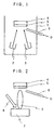
- Fig. 1 is a typical explanatory view forming a YMnO 3 by using a vacuum depositing reactor, for example, called an MBE (Molecular Beam Epitaxy) method.
- 1 is a vacuum chamber.
- 2 are respective material sources filled with Y and Mn, having a heater, a shutter, and the like, not shown.
- 4 is a substrate formed, for example, of silicon on which a ferroelectric film is to be formed.
- 5 is a YMnO 3 film-formed on a surface of the substrate 4.
- 6 is an oxidizing source supply passage for supplying an oxygen source such as oxygen, ozone, or the like.
- a substrate 4 on which a ferroelectric film is formed is set within the vacuum chamber 1, and Y and Mn are respectively filled in crucibles of the material sources 2, 3.
- the vacuum chamber 1 is evacuated down to an oxygen partial pressure of 10 -9 Torr or lower.
- the substrate 4 is heated up to approximately 700 °C and Y and Mn are brought into a molten state. Thereafter, an oxygen source is blown to over the surface of the substrate. Y and Mn are scattered toward the substrate 4 by opening the shutters in the material sources 2, 3.
- the oxygen partial pressure is held at approximately 10 -4 to 10 -6 Torr.
- the present invention is characterized by blowing an oxidizing source directly over the surface of the substrate 4 and reducing an oxide partial pressure to approximately 10 -3 Torr or lower, preferably 10 -6 Torr or lower, within the vacuum chamber 1.
- an oxygen source increases the oxygen partial pressure to approximately 10 -8 Torr or higher. That is, it is usual practice for vacuum deposition to carry out in a state of an oxygen partial pressure of higher than approximately 10 -2 Torr. In a state of a high oxygen partial pressure, however, Y and Mn oxidize in a state of the material source 2, 3 or during travel from the material source 2, 3 to the surface of the substrate 4, as stated before.
- the elements, such as Y and Mn, ready to oxidize will not turn into an oxide before reaching the substrate 4.
- Y and Mn are oxidized by the oxygen supplied over the substrate 4 while depositing thereon, and accordingly a YMnO 3 crystalline structure is created and film-formed on the substrate 4.
- the oxygen partial pressure is 10 -6 Torr or lower as stated before.
- Y and Mn can respectively prevented from oxidizing, and a YMnO 3 oxide is created due to supply of oxygen to the surface of the substrate 4.
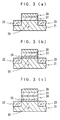
- Fig. 2 is a typical explanatory view of forming a YMnO 3 film by a laser abrasion method.
- Figs. 2, 4 to 6 refer to a same part of Fig. 1.
- 7 is a non-oxide target such as of a Y-Mn alloy, for example.
- 8 is a laser light source which may use a excimer laser having a laser beam, for example, of an energy density of 0.5 - 2 J/cm 2 with a pulse of 5 - 20 Hz.
- 9 represents a bloom occurring upon irradiating a laser pulse to the target 7.
- This laser abrasion method is characterized by using a Y-Mn alloy as a non-oxide target and an oxygen source is blown to over a film forming surface of the substrate 4 so as to form an oxide thin film. That is, the use of an oxide target causes the target to vary in composition, whereas the use of the non-oxide target of the present invention will not change the composition of the target thereby forming a ferroelectric film excellent in crystallinity.
- the oxygen partial pressure was reduced to approximately 10 -4 - 10 -5 Torr within the growth chamber, and the substrate 4 was raised to a temperature of approximately 700 °C to grow the laser beam to 24000 pulses.
- a ferroelectric thin-film of a YMnO 3 crystal was formed in a thickness of approximately 0.3 - 1 ⁇ m.
- prevention has to be given against the target oxidation and the accompanying composition change, similarly to the above-described vacuum deposition. Further, Y and Mn must not be individually oxidized during sputtering from the target to the substrate surface.
- the inside of the film-forming reactor is reduced in pressure to 10 -2 Torr or lower, more preferably 10 -4 Torr or lower and the oxygen partial pressure is given at 10 -8 Torr and higher.
- a ferroelectric film can be grown on the surface of the substrate 4 while blowing an oxygen source to the surface of the substrate 4.
- the film-forming method by sputter uses a reactor similar, in a typical view, to the reactor of Fig. 2.
- this method is different in that an inert gas atmosphere such as of Ar is used in place of irradiating a laser beam so that the inert gas is ionised by applying a high voltage between the substrate to thereby cause the element of the target sputtering.
- This method is also characterized by using a non-oxide for the target 7 and the oxygen partial pressure is reduced to 10 -4 Torr within the film-forming reactor so that the film-forming surface is blown with an oxidation source to form a film thereon.
- the film was formed by raising the substrate temperature to approximately 700 °C due to a magnetron sputter method, for example, with an RF output of 75W with the oxygen partial pressure given at 10 -3 -10 -4 .
- the use of the non-oxide target of the present invention did not cause change of composition in the target, similarly to the laser abrasion case.
- a dielectric film could be formed with high crystallinity.
- the lower limit of the oxygen partial pressure is preferably 10 -8 Torr or higher.
- the present inventors has further eagerly studied to improve such characteristics as leak current reduction for applications in memories and thin-film capacitors.
- a Y/Mn atomic ratio of greater than 1 and smaller than 1.2 or smaller than 1 and greater than 0.8
- the surface is suppressed from being formed with an amorphous layer to provide grains with fineness and homogeneity, lessening frequency dispersions in dielectric constant as well as reducing current leaks.
- This is attributable to the fact that the ReMnO 3 is low in bandgap and the existence of somewhat carriers increases current leakage.
- Y and Mn in the material sources may be controlled in evaporating amount for the vacuum deposition method while the ratio of the both may be controlled during making a target for the laser abrasion method or the sputter method.
- This provides a ferroelectric film having a basic YMnO 3 structure having a same composition as the target but deviated in a Y-Mn ratio.
- an ReMnO 3 thin film of a ferroelecric film is in a p-type and current leakage can be reduced by adding a 4-valence element or substituting part of Re with a 4-valence element. That is, the ferroelectric films formed in the above-stated methods were measured of electromotive force by both a thermal probe method and a method utilizing a Hall effect. As a result, it was revealed that ReMnO 3 in the conventional form is in a p-type but the p-type disappeared from the observation when a 4-valence element was added.
- the resulting ReMnO 3 has a fine and homogeneous texture to thereby reduce current leak despite it is low in bandgap to readily increase current leak.
- the vacuum deposition method may be further prepared with a material source for a 4-valence element such as La so that the element is evaporated, together with Y and Mn, under control of evaporation amount.
- a 4-valence element such as La may be further added to Y and Mn when preparing a Y-Mn alloy target. Otherwise, the method is similarly carried out by using a target formed of a Y-Mn-La alloy having a content reduced of a 4-valence element such as La.
- a ferroelectric film having a basic YMnO 3 structure wherein a 4-valence element added thereto or part of Y is substituted by a 4-valence element. That is, in also this case, if an oxide target is employed, the presence of oxygen on the target surface causes Y precipitate on the surface of target so that the film composition becomes considerably excessive in Y, worsening the reproducibility of growth conditions.
- a non-oxide target is free from phenomenon such as composition change, making it possible to stably forming a well-crystallinity ferroelectric film.
- the material source metals are evaporated by differing the evaporation amount between Re and Mn, and/or by increasing the content of one of Re and Mn in excess of that of the other to a limit of 20 at. % and adding a 4-valence element as a part of Re and Mn. This enables formation, on the substrate surface, of a ferroelectric material having a basic ReMnO 3 structure wherein a 4-valence element is further added or part of Re is replaced by the 4-valence element.
- a ferroelectric material having a basic structure of ReMnO 3 can be film-formed on the surface of the substrate by a laser abrasion, wherein the material contains Re and Mn one of which is in excess than the other to a limit of 20 at. % and/or has a composition further added with a 4-valence element or part of Re is substituted by the 4-valence element.
- This uses a method of forming a ferroelectric material by laser abrasion, comprising placing a target and a film-forming substrate to oppositely within a reactor, wherein the target is formed different in content ratio between Re and Mn, or added with a 4-valence element.
- a ferroelectric material having a basic structure of ReMnO 3 can be film-formed on the surface of the substrate by sputtering, wherein the material contains Re and Mn one of which is in excess than the other to a limit of 20 at. % and/or has a composition further added with a 4-valence element or part of Re is substituted by the 4-valence element.
- This uses a method of forming a ferroelectric material by placing a target and a film-forming substrate oppositely, wherein the target is formed different in content ratio between Re and Mn, and/or further added with a 4-valence element.
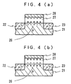
- FIG. 3 is a view showing a structural example of a semiconductor memory device using a ferroelectric film.
- the structure in Fig. 3(a) shows an example of a semiconductor memory device of a MFS structure having a semiconductor substrate 21 formed with a source region 22 and a drain region 23 sandwiching therebetween a channel region 26 on which a ferroelectric film 27 is directly formed to have a gate electrode 28 provided thereon.
- a ferroelectric film according to the invention is preferably applied to this structure of the semiconductor memory device, because it reduces a native oxide film existing at an interfacial portion between the ferroelectric film and the semiconductor substrate. This makes it possible to effectively apply voltages across the ferroelectric film.
- the structure in Fig. 3(b) shows also an example of a semiconductor memory device of an MFIS structure having a semiconductor substrate 21 formed with a channel region 26 on which a ferroelectric film 27 and a gate electrode 28 are formed through a gate dielectric film 25 formed of usual SiO 2 .
- the ferroelectric film 27 of the invention has a basic ReMnO 3 structure with a specific dielectric coefficient as low as approximately 20.
- the gate dielectric film 25 consumes a greater part of the voltage applied to the gate electrode 28.
- the voltage is sufficiently allocated to the ferroelectric film 27, and accordingly there is no necessity of excessively raising a voltage during writing in.
- Fig. 3(c) shows, similarly to Fig. 3(a), an example of a semiconductor memory device of an MFMIS structure having a semiconductor substrate 21 formed with a channel region 26 on which a floating gate 24 is provided through usual SiO 2 , wherein a ferroelectric film 27 and a gate electrode 28 are formed on the floating gate.
- the floating gate 24 can use ZnO doped with a 3-valence element.
- ZnO is easy to c-axis align on a substrate of a variety of types. Accordingly, it is easy to obtain a ferroelectric film having a basic ReMnO 3 structure on the substrate, which has a good crystallinity and hence an excellent ferroelectric characteristic.
- the ferroelectric film can be formed by adopting any of the method stated before.
- the ferroelectric film may be patterned by an RIE method or the like after forming the film, or by a lift-off technique.
- the source and drain regions for an FET may be formed by introducing an impurity prior to forming a ferroelectric film, or by self-alignment after forming a ferroelectric film and a gate electrode.
- the basic structure has Re and Mn one of which has a content in excess of the other to a limit in atomic ratio of 0.2 instead of 1, and or the basic structure has a ReMnO 3 material added with a 4-valence element. Accordingly, the ferroelectric material reduces the leak current as a defect of ReMnO 3 , and provides a ferroelectric film with enhanced characteristics with utilizing advantages given by the ReMnO 3 in nature. It is therefore possible to provide, at low cost, high-performance electronic components, such as semiconductor memory devices and thin-film capacitors, utilizing a ferroelectric film.
- the oxygen partial pressure as a film-forming condition is lower than the film-forming condition for a usual oxide, and a film is formed while blowing oxidation source such as oxygen or ozone only to a film-forming surface of a substrate. Accordingly, the evaporation source or the target is prevented from oxidizing or deviating of composition, thereby enabling stable growth. As a result, a ferroelectric film excellent in crystallinity and high in quality is obtained without encountering an amorphous texture. It is possible for semiconductor memories and thin-film capacitors to provide a ferroelectric film with a basic ReMnO 3 structure excellent in ferroelectric characteristics.
- a ferroelectric film having a basic ReMnO 3 structure excellent in crystallinity is employed which is small in dielectric constant.
- the ferroelectric film is adequately applied with a voltage even through a dielectric film.
- the ferroelectric film, difficult to pattern, can be formed on a dielectric film.
- a high performance semiconductor memory device is obtainable at low cost.
- the present invention a ferroelectric film low in dielectric constant and excellent in crystallinity is obtainable. Therefore, the invention is applicable to nonvolatile semiconductor memory devices utilizing a ferroelectric film, thin-film capacitors, etc.
Landscapes
- Chemical & Material Sciences (AREA)
- Organic Chemistry (AREA)
- Engineering & Computer Science (AREA)
- Materials Engineering (AREA)
- Metallurgy (AREA)
- Inorganic Chemistry (AREA)
- Crystallography & Structural Chemistry (AREA)
- Mechanical Engineering (AREA)
- Chemical Kinetics & Catalysis (AREA)
- Life Sciences & Earth Sciences (AREA)
- General Life Sciences & Earth Sciences (AREA)
- Geology (AREA)
- Non-Volatile Memory (AREA)
- Semiconductor Memories (AREA)
- Physical Vapour Deposition (AREA)
- Inorganic Insulating Materials (AREA)
- Formation Of Insulating Films (AREA)
Abstract
Description
Claims (19)
- A ferroelectric material having a basic structure of ReMnO3, said ferroelectric material comprises Re and Mn one of which is contained in excess of the other to a limit of 20 at. %.
- A ferroelectric material having a basic structure of ReMnO3, said ferroelectric material is further added with a 4-valence element or part of Re is substituted by a 4-valence element.
- A ferroelectric material according to claim 2, wherein the 4-valence element is La.
- A ferroelectric material according to claim 2 or 3, wherein one of Re and Mn is contained in excess of the other to a limit of 20 at. %.
- A method of forming a ferroelectric material, characterized by:placing material sources of Re and Mn opposite to a substrate to be formed with a ferroelectric film within a vacuum deposition reactor;controlling an oxygen partial pressure within said vacuum deposition reactor at 10-3 Torr or lower;evaporating metals of said material sources while blowing an oxidizing source to the film forming surface of said substrate;whereby a ferroelectric material having a basic structure of ReMnO3 is film-formed on the surface of said substrate.
- A method of forming a ferroelectric material according to claim 5, wherein the oxygen partial pressure is 10-6 Torr or lower.
- A method according to claim 5 or 6, wherein the ferroelectric material is film-formed by differing evaporation amounts between Re and Mn so that one of Re and Mn is contained in excess of the other to a limit of 20 at. %.
- A method according to claim 5, 6 or 7, wherein the ferroelectric material is film-formed by adding a 4-valence element to said evaporation sources, so that the material having the basic structure of ReMnO3 is further added by the 4-valence element or substituted in part of Re by the 4-valence element.
- A method of forming a ferroelectric material by placing a target and a substrate oppositely within a reactor to form a ferroelectric film on said substrate by laser abrasion, characterized by:using a non-oxide target formed of an alloy of Re and Mn as said target material;controlling an oxygen partial pressure to 10-2 Torr or lower;irradiating laser to said target while blowing an oxidizing source to a film-forming surface of said substrate;whereby a ferroelectric material having a basic structure of ReMnO3 is film-formed on the surface of said substrate.
- A method according to claim 9, wherein the ferroelectric material is film-formed by differing a content ratio between Re and Mn so that one of Re and Mn is contained in excess of the other to a limit of 20 at. %.
- A method according to claim 9 or 10, wherein the ferroelectric material is film-formed by adding a 4-valence element to said target, so that the material having the basic structure of ReMnO3 is further added by the 4-valence element or substituted in part of Re by the 4-valence element.
- A method of forming a ferroelectric film by placing a target and a substrate oppositely within a reactor to form a ferroelectric film on said substrate by sputtering, characterized by:using a non-oxide target formed of an alloy of Re and Mn as said target;controlling an oxygen partial pressure to 10-4 Torr or lower;applying a voltage to said target while blowing an oxidizing source to a film-forming surface of said substrate;whereby a ferroelectric material having a basic structure of ReMnO3 is film-formed on the surface of said substrate.
- A method according to claim 12, wherein the ferroelectric material is film-formed by differing a content ratio between Re and Mn so that one of Re and Mn is contained in excess of the other to a limit of 20 at. %.
- A method according to claim 12 or 13, wherein the ferroelectric material is film-formed by adding a 4-valence element to said target, so that the material having the basic structure of ReMnO3 is further added by the 4-valence element or substituted in part of Re by the 4-valence element.
- A semiconductor memory device, having a ferroelectric film on a semiconductor substrate surface side, wherein said ferroelectric film comprises a ferroelectric material having a basic structure of ReMnO3 having Re and Mn one of which is contained in excess of the other to a limit of 20 at. %.
- A semiconductor memory device, having a ferroelectric film on a semiconductor substrate surface side, wherein said ferroelectric film comprises a basic structure of ReMnO3 further added with a 4-valence element.
- A method of manufacturing a semiconductor memory device having a ferroelectric film on a semiconductor substrate surface side, characterized by:placing material sources of Re and Mn opposite to a substrate to be formed with a ferroelectric film within a vacuum deposition reactor;controlling an oxygen partial pressure within said vacuum deposition reactor to 10-3 Torr or lower;evaporating metals of said material sources while blowing an oxidizing source to the film forming surface of said substrate.
- A method of manufacturing a semiconductor memory device having a ferroelectric film on a semiconductor substrate surface side, characterized by:placing a non-oxide target of an alloy of Re and Mn and a semiconductor substrate oppositely within a reactor;controlling an oxygen partial pressure within said reactor to 10-2 Torr or lower;irradiating laser to said target while blowing an oxidizing source to the film forming surface of said semiconductor substrate;whereby a ferroelectric material having a basic structure of ReMnO3 is film-formed on the surface of said substrate.
- A method of manufacturing a semiconductor memory device having a ferroelectric film on a semiconductor substrate surface side, characterized by:placing a non-oxide target of an alloy of Re and Mn and a semiconductor substrate oppositely within a reactor;controlling an oxygen partial pressure within said reactor to 10-4 Torr or lower;applying a voltage to said target to cause sputtering while blowing an oxidizing source to a film forming surface of said semiconductor substrate;whereby a, ferroelectric material having a basic structure of ReMnO3 is film-formed on the surface of said semiconductor substrate.
Applications Claiming Priority (9)
| Application Number | Priority Date | Filing Date | Title |
|---|---|---|---|
| JP256017/96 | 1996-09-27 | ||
| JP256014/96 | 1996-09-27 | ||
| JP8256014A JPH10101428A (en) | 1996-09-27 | 1996-09-27 | Strong dielectric material, production thereof and semiconductor memory device |
| JP8256017A JPH10101431A (en) | 1996-09-27 | 1996-09-27 | Production of strong dielectric material, semiconductor memory device and production thereof |
| JP8256016A JPH10101430A (en) | 1996-09-27 | 1996-09-27 | Production of strong dielectric material, semiconductor memory device and production thereof |
| JP256016/96 | 1996-09-27 | ||
| JP256015/96 | 1996-09-27 | ||
| JP25601596A JP3966928B2 (en) | 1996-09-27 | 1996-09-27 | Ferroelectric material manufacturing method and semiconductor memory device |
| PCT/JP1997/003455 WO1998013300A1 (en) | 1996-09-27 | 1997-09-26 | Ferroelectric material, method of manufacturing the same, semiconductor memory, and method of manufacturing the same |
Publications (3)
| Publication Number | Publication Date |
|---|---|
| EP0864537A1 true EP0864537A1 (en) | 1998-09-16 |
| EP0864537A4 EP0864537A4 (en) | 2001-07-11 |
| EP0864537B1 EP0864537B1 (en) | 2007-01-24 |
Family
ID=27478383
Family Applications (1)
| Application Number | Title | Priority Date | Filing Date |
|---|---|---|---|
| EP97941264A Expired - Lifetime EP0864537B1 (en) | 1996-09-27 | 1997-09-26 | Ferroelectric material, method of manufacturing the same, semiconductor memory, and method of manufacturing the same |
Country Status (6)
| Country | Link |
|---|---|
| US (1) | US6245451B1 (en) |
| EP (1) | EP0864537B1 (en) |
| KR (1) | KR100490518B1 (en) |
| CA (1) | CA2238857C (en) |
| DE (1) | DE69737283T2 (en) |
| WO (1) | WO1998013300A1 (en) |
Families Citing this family (12)
| Publication number | Priority date | Publication date | Assignee | Title |
|---|---|---|---|---|
| JP3704258B2 (en) * | 1998-09-10 | 2005-10-12 | 松下電器産業株式会社 | Thin film formation method |
| KR20030041974A (en) * | 2000-08-24 | 2003-05-27 | 코바 테크놀로지스, 인크. | Single transistor rare earth manganite ferroelectric nonvolatile memory cell |
| WO2002071477A1 (en) | 2001-03-02 | 2002-09-12 | Cova Technologies Incorporated | Single transistor rare earth manganite ferroelectric nonvolatile memory cell |
| US6825517B2 (en) * | 2002-08-28 | 2004-11-30 | Cova Technologies, Inc. | Ferroelectric transistor with enhanced data retention |
| US6888736B2 (en) | 2002-09-19 | 2005-05-03 | Cova Technologies, Inc. | Ferroelectric transistor for storing two data bits |
| US6714435B1 (en) * | 2002-09-19 | 2004-03-30 | Cova Technologies, Inc. | Ferroelectric transistor for storing two data bits |
| TWI226377B (en) * | 2002-11-08 | 2005-01-11 | Ind Tech Res Inst | Dielectric material compositions |
| US8256386B2 (en) * | 2009-01-08 | 2012-09-04 | Honda Motor Co., Ltd. | Saddle-ride vehicle |
| US9378760B2 (en) | 2014-07-31 | 2016-06-28 | Seagate Technology Llc | Data reader with tuned microstructure |
| EP3182048A1 (en) | 2015-12-16 | 2017-06-21 | Alfa Laval Corporate AB | Porthole gasket, assembly for a heat exchanger and heat exchanger comprising such an assembly |
| US10615176B2 (en) | 2017-11-22 | 2020-04-07 | International Business Machine Corporation | Ferro-electric complementary FET |
| KR102050034B1 (en) | 2018-03-22 | 2019-11-28 | 서울대학교산학협력단 | Material for nonvolatile memory device and method of manufacturing the same |
Family Cites Families (10)
| Publication number | Priority date | Publication date | Assignee | Title |
|---|---|---|---|---|
| US3884837A (en) * | 1973-07-02 | 1975-05-20 | Bell Telephone Labor Inc | Catalyst containing a perovskite-like manganite |
| JPH05255838A (en) * | 1992-03-12 | 1993-10-05 | Mitsubishi Electric Corp | Method for forming oxide thin film and device therefor |
| US5487356A (en) * | 1992-08-07 | 1996-01-30 | Advanced Technology Materials, Inc. | Chemical vapor deposition method of growing oxide films with giant magnetoresistance |
| DE4310318C2 (en) * | 1993-03-30 | 1998-12-03 | Siemens Ag | Use of a material with a perovskite-like crystal structure and increased magnetoresistive effect, and method for producing the material |
| DE4323821A1 (en) * | 1993-07-15 | 1995-01-19 | Siemens Ag | Pyrodetector element with oriented grown pyroelectric layer and method for its production |
| JP3223233B2 (en) * | 1994-08-17 | 2001-10-29 | ティーディーケイ株式会社 | Oxide thin film, substrate for electronic device, and method of forming oxide thin film |
| JP2685721B2 (en) * | 1994-11-04 | 1997-12-03 | 工業技術院長 | Grain-free boundary type manganese oxide based crystal and switching type magnetoresistive element |
| JPH08162614A (en) * | 1994-12-01 | 1996-06-21 | Tdk Corp | Mis capacitor and its manufacture |
| JP3137880B2 (en) * | 1995-08-25 | 2001-02-26 | ティーディーケイ株式会社 | Ferroelectric thin film, electronic device, and method of manufacturing ferroelectric thin film |
| JP3286181B2 (en) * | 1995-11-17 | 2002-05-27 | ティーディーケイ株式会社 | Recording medium, method of manufacturing the same, and information processing apparatus |
-
1997
- 1997-09-26 US US09/068,996 patent/US6245451B1/en not_active Expired - Fee Related
- 1997-09-26 WO PCT/JP1997/003455 patent/WO1998013300A1/en not_active Ceased
- 1997-09-26 DE DE69737283T patent/DE69737283T2/en not_active Expired - Fee Related
- 1997-09-26 EP EP97941264A patent/EP0864537B1/en not_active Expired - Lifetime
- 1997-09-26 CA CA002238857A patent/CA2238857C/en not_active Expired - Fee Related
- 1997-09-26 KR KR10-1998-0703890A patent/KR100490518B1/en not_active Expired - Fee Related
Also Published As
| Publication number | Publication date |
|---|---|
| US6245451B1 (en) | 2001-06-12 |
| DE69737283T2 (en) | 2007-11-15 |
| EP0864537B1 (en) | 2007-01-24 |
| WO1998013300A1 (en) | 1998-04-02 |
| DE69737283D1 (en) | 2007-03-15 |
| EP0864537A4 (en) | 2001-07-11 |
| KR100490518B1 (en) | 2005-09-09 |
| CA2238857C (en) | 2002-11-19 |
| CA2238857A1 (en) | 1998-04-02 |
| KR19990071614A (en) | 1999-09-27 |
Similar Documents
| Publication | Publication Date | Title |
|---|---|---|
| US5955213A (en) | Ferroelectric thin film, electric device, and method for preparing ferroelectric thin film | |
| US6096434A (en) | Film structure, electronic device, recording medium, and method for forming conductive oxide thin films | |
| KR101078509B1 (en) | Method of manufacturing thin film transistor | |
| US6245451B1 (en) | Ferroelectric material, method of manufacturing the same, semiconductor memory, and method of manufacturing the same | |
| US5810923A (en) | Method for forming oxide thin film and the treatment of silicon substrate | |
| US6121647A (en) | Film structure, electronic device, recording medium, and process of preparing ferroelectric thin films | |
| US20040224459A1 (en) | Layered structure, method for manufacturing the same, and semiconductor element | |
| EP1209729A1 (en) | Multilayered body, method for fabricating multilayered body, and semiconductor device | |
| Shogo Imada et al. | Epitaxial growth of ferroelectric YMnO3 thin films on Si (111) substrates by molecular beam epitaxy | |
| Basit et al. | Growth of highly oriented pb (zr, ti) o 3 films on mgo-buffered oxidized si substrates and its application to ferroelectric nonvolatile memory field-effect transistors | |
| JPH10313097A (en) | Ferroelectric thin film, manufacturing method and device comprising ferroelectric thin film | |
| US6307225B1 (en) | Insulating material, substrate covered with an insulating film, method of producing the same, and thin-film device | |
| KR100969807B1 (en) | Resistance change memory device having a reactive metal film and a method of operating the same | |
| JP3222569B2 (en) | Semiconductor storage element | |
| KR20050106391A (en) | (001)-orientated perovskite film formation method and device having perovskite film | |
| JP3966928B2 (en) | Ferroelectric material manufacturing method and semiconductor memory device | |
| JPH10101428A (en) | Strong dielectric material, production thereof and semiconductor memory device | |
| JP3746815B2 (en) | Semiconductor memory device | |
| JP3403507B2 (en) | Ferroelectric memory element and method of manufacturing the same | |
| JPH10101430A (en) | Production of strong dielectric material, semiconductor memory device and production thereof | |
| Tokumitsu et al. | Characterization of Pb (ZrxTi1− x) O3 films prepared by vacuum evaporation method | |
| Sudhama et al. | Thickness-scaling of sputtered PZT films in the 200 nm range for memory applications | |
| JP3813206B2 (en) | Method for manufacturing ferroelectric memory element | |
| Imada et al. | MBE growth of ferroelectric YMnO3 thin films on Si (111) using Y2O3 buffer layers | |
| JPH07193135A (en) | Method for manufacturing dielectric thin film and field effect transistor |
Legal Events
| Date | Code | Title | Description |
|---|---|---|---|
| PUAI | Public reference made under article 153(3) epc to a published international application that has entered the european phase |
Free format text: ORIGINAL CODE: 0009012 |
|
| 17P | Request for examination filed |
Effective date: 19980716 |
|
| AK | Designated contracting states |
Kind code of ref document: A1 Designated state(s): DE GB |
|
| A4 | Supplementary search report drawn up and despatched |
Effective date: 20010530 |
|
| AK | Designated contracting states |
Kind code of ref document: A4 Designated state(s): DE GB |
|
| RIC1 | Information provided on ipc code assigned before grant |
Free format text: 7C 01G 45/00 A, 7C 23C 14/08 B |
|
| 17Q | First examination report despatched |
Effective date: 20021217 |
|
| GRAP | Despatch of communication of intention to grant a patent |
Free format text: ORIGINAL CODE: EPIDOSNIGR1 |
|
| GRAS | Grant fee paid |
Free format text: ORIGINAL CODE: EPIDOSNIGR3 |
|
| GRAA | (expected) grant |
Free format text: ORIGINAL CODE: 0009210 |
|
| AK | Designated contracting states |
Kind code of ref document: B1 Designated state(s): DE GB |
|
| REG | Reference to a national code |
Ref country code: GB Ref legal event code: FG4D |
|
| REF | Corresponds to: |
Ref document number: 69737283 Country of ref document: DE Date of ref document: 20070315 Kind code of ref document: P |
|
| PLBE | No opposition filed within time limit |
Free format text: ORIGINAL CODE: 0009261 |
|
| STAA | Information on the status of an ep patent application or granted ep patent |
Free format text: STATUS: NO OPPOSITION FILED WITHIN TIME LIMIT |
|
| 26N | No opposition filed |
Effective date: 20071025 |
|
| PGFP | Annual fee paid to national office [announced via postgrant information from national office to epo] |
Ref country code: DE Payment date: 20081002 Year of fee payment: 12 |
|
| PGFP | Annual fee paid to national office [announced via postgrant information from national office to epo] |
Ref country code: GB Payment date: 20081001 Year of fee payment: 12 |
|
| GBPC | Gb: european patent ceased through non-payment of renewal fee |
Effective date: 20090926 |
|
| PG25 | Lapsed in a contracting state [announced via postgrant information from national office to epo] |
Ref country code: DE Free format text: LAPSE BECAUSE OF NON-PAYMENT OF DUE FEES Effective date: 20100401 |
|
| PG25 | Lapsed in a contracting state [announced via postgrant information from national office to epo] |
Ref country code: GB Free format text: LAPSE BECAUSE OF NON-PAYMENT OF DUE FEES Effective date: 20090926 |