EP0856952A2 - A method and a circuit arrangement for the processing of received signals in a telecommunication system - Google Patents
A method and a circuit arrangement for the processing of received signals in a telecommunication system Download PDFInfo
- Publication number
- EP0856952A2 EP0856952A2 EP98660008A EP98660008A EP0856952A2 EP 0856952 A2 EP0856952 A2 EP 0856952A2 EP 98660008 A EP98660008 A EP 98660008A EP 98660008 A EP98660008 A EP 98660008A EP 0856952 A2 EP0856952 A2 EP 0856952A2
- Authority
- EP
- European Patent Office
- Prior art keywords
- signal
- band
- intermediate frequency
- digital
- pass
- Prior art date
- Legal status (The legal status is an assumption and is not a legal conclusion. Google has not performed a legal analysis and makes no representation as to the accuracy of the status listed.)
- Granted
Links
Images


Classifications
-
- H—ELECTRICITY
- H04—ELECTRIC COMMUNICATION TECHNIQUE
- H04B—TRANSMISSION
- H04B1/00—Details of transmission systems, not covered by a single one of groups H04B3/00 - H04B13/00; Details of transmission systems not characterised by the medium used for transmission
- H04B1/0003—Software-defined radio [SDR] systems, i.e. systems wherein components typically implemented in hardware, e.g. filters or modulators/demodulators, are implented using software, e.g. by involving an AD or DA conversion stage such that at least part of the signal processing is performed in the digital domain
- H04B1/0007—Software-defined radio [SDR] systems, i.e. systems wherein components typically implemented in hardware, e.g. filters or modulators/demodulators, are implented using software, e.g. by involving an AD or DA conversion stage such that at least part of the signal processing is performed in the digital domain wherein the AD/DA conversion occurs at radiofrequency or intermediate frequency stage
-
- H—ELECTRICITY
- H03—ELECTRONIC CIRCUITRY
- H03D—DEMODULATION OR TRANSFERENCE OF MODULATION FROM ONE CARRIER TO ANOTHER
- H03D7/00—Transference of modulation from one carrier to another, e.g. frequency-changing
- H03D7/16—Multiple-frequency-changing
- H03D7/161—Multiple-frequency-changing all the frequency changers being connected in cascade
-
- H—ELECTRICITY
- H04—ELECTRIC COMMUNICATION TECHNIQUE
- H04B—TRANSMISSION
- H04B1/00—Details of transmission systems, not covered by a single one of groups H04B3/00 - H04B13/00; Details of transmission systems not characterised by the medium used for transmission
- H04B1/0003—Software-defined radio [SDR] systems, i.e. systems wherein components typically implemented in hardware, e.g. filters or modulators/demodulators, are implented using software, e.g. by involving an AD or DA conversion stage such that at least part of the signal processing is performed in the digital domain
-
- H—ELECTRICITY
- H04—ELECTRIC COMMUNICATION TECHNIQUE
- H04B—TRANSMISSION
- H04B1/00—Details of transmission systems, not covered by a single one of groups H04B3/00 - H04B13/00; Details of transmission systems not characterised by the medium used for transmission
- H04B1/005—Details of transmission systems, not covered by a single one of groups H04B3/00 - H04B13/00; Details of transmission systems not characterised by the medium used for transmission adapting radio receivers, transmitters andtransceivers for operation on two or more bands, i.e. frequency ranges
- H04B1/0053—Details of transmission systems, not covered by a single one of groups H04B3/00 - H04B13/00; Details of transmission systems not characterised by the medium used for transmission adapting radio receivers, transmitters andtransceivers for operation on two or more bands, i.e. frequency ranges with common antenna for more than one band
- H04B1/0057—Details of transmission systems, not covered by a single one of groups H04B3/00 - H04B13/00; Details of transmission systems not characterised by the medium used for transmission adapting radio receivers, transmitters andtransceivers for operation on two or more bands, i.e. frequency ranges with common antenna for more than one band using diplexing or multiplexing filters for selecting the desired band
-
- H—ELECTRICITY
- H04—ELECTRIC COMMUNICATION TECHNIQUE
- H04B—TRANSMISSION
- H04B1/00—Details of transmission systems, not covered by a single one of groups H04B3/00 - H04B13/00; Details of transmission systems not characterised by the medium used for transmission
- H04B1/005—Details of transmission systems, not covered by a single one of groups H04B3/00 - H04B13/00; Details of transmission systems not characterised by the medium used for transmission adapting radio receivers, transmitters andtransceivers for operation on two or more bands, i.e. frequency ranges
- H04B1/0053—Details of transmission systems, not covered by a single one of groups H04B3/00 - H04B13/00; Details of transmission systems not characterised by the medium used for transmission adapting radio receivers, transmitters andtransceivers for operation on two or more bands, i.e. frequency ranges with common antenna for more than one band
- H04B1/006—Details of transmission systems, not covered by a single one of groups H04B3/00 - H04B13/00; Details of transmission systems not characterised by the medium used for transmission adapting radio receivers, transmitters andtransceivers for operation on two or more bands, i.e. frequency ranges with common antenna for more than one band using switches for selecting the desired band
-
- H—ELECTRICITY
- H04—ELECTRIC COMMUNICATION TECHNIQUE
- H04B—TRANSMISSION
- H04B1/00—Details of transmission systems, not covered by a single one of groups H04B3/00 - H04B13/00; Details of transmission systems not characterised by the medium used for transmission
- H04B1/06—Receivers
- H04B1/16—Circuits
- H04B1/26—Circuits for superheterodyne receivers
-
- H—ELECTRICITY
- H04—ELECTRIC COMMUNICATION TECHNIQUE
- H04B—TRANSMISSION
- H04B1/00—Details of transmission systems, not covered by a single one of groups H04B3/00 - H04B13/00; Details of transmission systems not characterised by the medium used for transmission
- H04B1/38—Transceivers, i.e. devices in which transmitter and receiver form a structural unit and in which at least one part is used for functions of transmitting and receiving
- H04B1/40—Circuits
- H04B1/403—Circuits using the same oscillator for generating both the transmitter frequency and the receiver local oscillator frequency
- H04B1/406—Circuits using the same oscillator for generating both the transmitter frequency and the receiver local oscillator frequency with more than one transmission mode, e.g. analog and digital modes
Definitions
- the object of the invention is a method and a circuit arrangement for the processing of a signal in connection with its reception, when the signal conforms to one or more system specifications.
- the invention is preferably applied in receivers operating on two frequency ranges or in receivers intended to be used in two radio communication systems.
- the receiver is a part of a mobile station or a base station of a cellular system.
- DSSS Direct Sequence Spread Spectrum
- FM frequency modulation
- UMTS Universal Mobile Telecommunications System
- ETSI European Telecommunications Standards Institute
- FPLMTS Future Public Land Mobile Telecommunications Systems
- a receiver operating in two systems must be able to process signals conforming to two different specifications.
- the signals of these systems may have different bit rates, signal bandwidths, and channel rasters.
- Channel raster means the frequency difference between two adjacent channels. For instance in the GSM system the signal bit rate is 270.833 kbit/s, the channel raster is 200 kHz, and the signal bandwidth is 200 kHz. On the other hand, for instance in the DECT system the bit rate is 1.152 Mbit/s, the channel raster is 1728 kHz and the signal bandwidth is about 1 MHz. In future systems, such as in e.g. the UMTS system, the bandwidth required for the transmission of a signal will probably be wider than in the GSM and DECT systems, due to the higher bit rate.
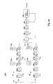
- Figure 1a shows a previously known circuit arrangement 100 for the reception of signals of two systems.
- the radio frequency (RF) signal Rx received via the antenna 101 is supplied into two receive branches A and B.
- the signal according to the system specification A is filtered in the band-pass filter 102a, amplified 104a and mixed to the intermediate frequency by the signal obtained from the oscillator 108a, so that the output of the mixer 106a provides the intermediate frequency signal IF1.
- the intermediate frequency signal is further supplied to the band-pass filter 110a, and the signal obtained from this is amplified 112a. Then this signal is mixed by a signal obtained from a second oscillator 116a, whereby the output of the mixer 114a provides a second intermediate frequency signal IF2.
- the second intermediate frequency signal is band-pass filtered 118a and amplified 120a.
- a signal according to the second system specification B is processed in the second signal branch B, which comprises units corresponding to those of the signal branch A: a band-pass filter 102b, an amplifier 104b, and a mixer 106b with an accompanying oscillator 108b, and a band-pass filter 110b, an amplifier 112b, and a mixer 114b with an accompanying oscillator 116b, and a band-pass filter 118b and an amplifier 120b.
- the signal according to the system specification A is prevented to propagate in the signal branch B, and the signal according to the system specification B is prevented to propagate in the signal branch A.
- the signal branch can be selected with a switch (not shown in figure 1) ) if the systems A and B use the same RF frequency band.
- the switch 122 selects either the signal from the signal branch A or the signal from the signal branch B to be supplied to the input of the analog-to-digital converter 124.
- the analog-to-digital converter 124 the signal is sampled into digital samples by a sampling frequency determined by the sampling signal f s .
- the signal converted into digital samples is further supplied to the digital signal processing unit 126, which i.a. performs signal detection and provides a digital baseband output signal, which further can be converted into an analog signal by a digital-to-analog converter (not shown in figure 1a).
- the signal selected for the analog-to-digital converter can be controlled in accordance with a change-over instruction transmitted by the mobile network. Then the signal processing unit detects this instruction and controls the switch 122 in the manner indicated by the instruction. If the mobile system permits the user of a mobile station to select the system he uses, then the processor of the mobile station generates a control instruction to the switch, based on an instruction given by the user via the a interface, such as a keyboard.
- Figure 1b shows the pass-band of the band-pass filter 102a, which is dimensioned according to the frequency range used in the system A.
- the filter 102a has a pass-band width B 11a and a center frequency F11a.
- figure 1c shows the pass-band of the band-pass filter 102b, which is dimensioned according to the frequency range used in the system B.
- the filter 102b has a pass-band width B11b and a center frequency F11b.
- Figure 1d shows the pass-band of the first intermediate frequency band-pass filter 110a in the signal branch A.
- the width of this pass-band is B12a and the center frequency F12a.
- figure le shows the pass-band of the first intermediate frequency band-pass filter 110b in the signal branch B.
- the width of this pass-band is B12b and the center frequency F12b.
- the figure 1f shows the pass-band of the second intermediate frequency band-pass filter 118a in the signal branch A, having a pass-band width B13a and the center frequency F13a.
- the figure 1g shows the pass-band of the second intermediate frequency band-pass filter 118b in the signal branch B, having a pass-band width B13b and the center frequency F13b.
- Figures 1d, le, 1f and 1g show that the pass-bands of the intermediate frequency band-pass filters are narrower in the signal branch A and wider in the signal branch B, according to the specifications of the systems A and B.
- the object of the invention is to create a simple solution for receiving the signals of different systems, when the received signals have different signal bandwidths.
- One idea of the invention is that before the analog-to-digital conversion the intermediate frequency signal is processed as a broadband signal in the same intermediate frequency signal line, so that the signals having different intermediate frequency bandwidths are within the pass-band of the signal line.
- the signal also contains other intermediate frequency signals than the received payload signal.
- the analog-to-digital conversion is made on a conversion range with a wide dynamics, so that also out-band signals can be converted without causing distortion components on the band of the received payload signal.
- the final bandwidth restriction is then performed by digital signal processing.
- the intermediate frequency signals have substantially the same center frequency, and they pass through the IF section at different times, except for signals of the CDMA system which can be separated.
- the invention It is not necessary to filter the intermediate frequency signal depending on the signal bandwidth, and therefore separately intermediate frequency filters are not required for each system. It is also possible to minimize the number of mixers, amplifiers and signal switches. Further it is possible to have a narrower dynamic operating range of the automatic gain control circuit or the AGC circuit, or the circuit could be omitted altogether. Thus a remarkably small-sized receiver is obtained, and savings are obtained in the manufacturing costs compared to prior art solutions. Further the receiver of the invention can also be used to receive signals of new systems, without changes in the intermediate frequency section.
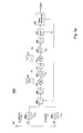
- FIG. 2a shows a block diagram 200 of the receiver in a combined telephone according to the invention, operating in two different communication systems.
- the RF signal Rx received via the antenna 201 is supplied to two reception branches A and B.
- a signal according to the system A specification is filtered in the band-pass filter 202a, amplified 204a and mixed to the intermediate frequency by the signal obtained from the oscillator 208a, so that the output of the mixer 206a provides an intermediate frequency signal IF1.
- the intermediate frequency signal is further supplied to the band-pass filter 210a, and the signal obtained from the filter is amplified 212a.
- the signal is mixed by a signal obtained from a second oscillator 216a, whereby the output of the mixer 214a provides a second intermediate frequency signal IF2.
- a signal according to the system B specification is processed in the second signal branch B, comprising units corresponding to those of the signal branch A: a band-pass filter 202b, an amplifier 204b and a mixer 206b with an accompanying oscillator 208b. and a band-pass filter 210b, an amplifier 212b, and a mixer 214b with an accompanying oscillator 216b.
- the switch 222 further selects for processing either the signal of the signal branch A or the signal of the signal branch B.
- the signal selected by the switch 222 is supplied to a band-pass filter, which according to the invention has a sufficiently wide pass-band, so that both the signal of the system A and the signal of the system B are within the pass-band of the filter. Then the signal is amplified 220 and supplied to the analog-to-digital converter 224, where the signal is sampled into digital samples by a sampling frequency determined by the sampling signal f s .
- the signal converted into digital samples is further supplied to the digital signal processing unit 226.
- the signal is digitally band-pass filtered according to the invention.
- the unit 226 also performs i.a. signal detection, and it provides a digital baseband output signal, which further can be converted into an analog signal by a digital-to-analog converter (not shown in figure 2a).
- the switch 222 is controlled in a corresponding manner as in the solution according to figure 1a.
- Figure 2b shows the pass-band of the band-pass filter 202a, which is dimensioned according to the frequency range used in the system A.
- the width of the pass-band of the filter 202a is B21a and its center frequency is F21a.
- figure 2c shows the pass-band of the band-pass filter 202b in the signal branch B, which is dimensioned according to the frequency range used in the system B.
- the pass-band width of the filter 202b is B21b and its center frequency is F21b.
- Figure 2d shows the pass-band of the first intermediate frequency band-pass filter 210a in the signal branch A.
- the width of this pass-band is B22a and the center frequency is F22a.
- figure 2e shows the pass-band of the first intermediate frequency band-pass filter 210b in the signal branch B.
- the width of this pass-band is B22b and the center frequency is F22b.
- the pass-bands of the above mentioned band-pass filters correspond to the pass-bands shown in figures 1b, 1c, 1d and 1e.
- FIG. 2f shows the pass-band of the second intermediate frequency band-pass filter 218 having the width B23 and the center frequency F23.
- the pass-band of the second intermediate frequency band-pass filter 218 is so wide that the signals of both system A and system B are within the pass-band. Because the final bandwidth restriction is performed in the digital signal processing unit, the arrangement according to the invention can use only one second intermediate frequency band-pass filter, or this filter could be omitted altogether.
- Figure 3a shows a block diagram of the receiver of a combination telephone according to the invention operating in the DECT and DCS systems. Below is first a description of the DECT and DCS system characteristics, and the application of the invention in said systems. Then there is a more detailed description of the circuit arrangement shown in figure 1a.
- the DCS system utilizes the GMSK modulation of the GSM system in which the signal bandwidth is about 200 kHz. The width of the received frequency range covering all channels is 75 MHz. In the DCS system the bit rate is 270.833 bit/s.
- the DECT system utilizes a non-linear GFSK modulation, in which the signal bandwidth is theoretically infinite, but in practice the bandwidth is about 1 MHz. In the DECT system the reception bandwidth is 20 MHz and the bit rate is 1.152 Mbit/s, as mentioned in the prior art description above.
- the signals of these systems having quite different operating principles can be received with one a single receiver according to the invention. where only the RF front-end sections are system dependent, due to the different signaling frequencies of the systems and their different RF signal tolerance requirements.
- the arrangement uses the same receiver structure for the processing of both signals, because the DCS system's reception bandwidth of 75 MHz can be filtered to 20 MHz, which is the reception bandwidth of the DECT system.
- both signals are supplied along the same signal line to the second mixer, which generates the second intermediate frequency.
- the second intermediate frequency is a broadband signal; its pass-band is at least 1 MHz.
- the receiver operates optimally both in the DECT system and in the DCS system.
- the RF signal Rx received via the antenna 301 is supplied to two band-pass filters 302a and 302b, whereby the signal according to the DECT system specification A is filtered in the band-pass filter 302a and the signal according to the DCS system specification B is filtered in the band-pass filter 302b. Then the switch 322 selects for further processing either the filtered signal of the A branch, or the filtered signal of the B branch.
- the signal selected by the switch 322 is amplified 304 and mixed to the intermediate frequency by the signal obtained from the oscillator 308 so that the output of the mixer 306 provides the intermediate frequency signal IF1.
- the intermediate frequency signal is further supplied to the band-pass filter 310, and the signal obtained from the filter is amplified 312. Then the signal is mixed by a signal obtained from the second oscillator 316, whereby the output of the mixer provides the second intermediate frequency signal IF2.
- the second intermediate frequency signal is supplied to the band-pass filter 318 and then the signal is amplified 320 and supplied to the analog-to-digital converter 324, in which the signal is sampled into digital samples by a sampling frequency determined by the sampling signal f s .
- the signal converted into digital samples is further supplied to the digital signal processing unit 326, which according to the invention performs the digital band-pass filtering of the signal.
- the unit 326 also performs i.a. signal detection, and this produces a digital baseband output signal, which further can be converted into an analog signal by a digital-to-analog converter (not shown in figure 3a).
- the switch 222 is controlled in a corresponding manner as in the solution according to figure 1a.
- Figure 3b shows the pass-band of the band-pass filter 302a, which is dimensioned according to the frequency range used in the DECT system (A).
- the width B31a of the pass-band of the filter 302a is then 20 MHz and the center frequency F31a is 1906 MHz.
- figure 3c shows the pass-band of the band-pass filter 302b in the signal branch B, which is dimensioned according to the frequency range used in the DCS system (B).
- the pass-band width B31b of the filter 302b is then 85 MHz and the center frequency F31b is 1848 MHz.
- Figure 3d shows the pass-band of the first intermediate frequency band-pass filter 310a.
- the width of this pass-band B32a is 20 MHz and the center frequency is F32a.
- figure 3e shows the pass-band of the second intermediate frequency band-pass filter 318 with the center frequency F33 and a pass-band B33 of 1.3 MHz.
- the pass-bands of the first and the second intermediate frequency band-pass filters are so wide that the signals of both the DECT system and the DCS system are within the pass-band of the filters.
- the final bandwidth restriction is made in the digital signal processing unit, it is possible in the arrangement according to the invention to use a single band-pass filter for the first intermediate frequency signal and a single band-pass filter for the second intermediate frequency signal, or these filters can even be omitted altogether.
- the circuit arrangement according to the invention utilizes an analog-to-digital converter operating on a dynamically wide conversion range. Then it is possible to convert a frequency range which is wider than the bandwidth of the payload signal, without causing distortion components in the signal's frequency band.
- the conversion dynamics of a typical wide bandwidth converter is about 80 to 90 dB. Then it is also possible to reduce the operating range of the automatic gain control circuit, or it can even be omitted altogether, as in the solutions shown in figures 2a and 3a.
- An advantage of a solution of this kind is also the good linearity of the receiver.
- the solutions according to the invention can be used in a mobile station of a system operating on two different frequency ranges, and in a mobile station operating on two different frequency ranges.
- the solution according to the invention can as well be used e.g. in a pager operating in two different paging systems, so the invention is not limited only to mobile stations.
- the communication systems and the frequency bands relating to them were described only as examples, and the application of the invention is in no way limited to the shown communication systems and the shown signal bands.
- the invention can be applied in all TDMA systems, such as in the GSM, DCS and DECT systems, and as well in the CDMA systems, such as in the IS-95 system. Further the invention can be used in planned future systems, such as in the UMTS system.
Abstract
Description
- an RF signal appearing in a predetermined frequency range is received,
- the received signal is converted into an intermediate frequency signal,
- said signal in the neighborhood of the intermediate frequency is converted into a digital sampled signal, and
- the digital sampled signal is digitally processed,
- means to receive an RF signal appearing in a predetermined frequency range,
- mixer means to convert the received signal into an intermediate frequency signal,
- an analog-to-digital converter to convert said intermediate frequency signal into a digital sampled signal, and
- signal processing means to process the digital sampled signal,
Claims (11)
- A method for the processing of a received signal, in whichcharacterized in that before said conversion into a digital sampled signal said intermediate frequency signal is processed on a pass-band (B23, B32, B33), which is substantially wider than the bandwidth of the received signal.an RF signal appearing in a predetermined frequency range is received.the received signal is converted into an intermediate frequency signal (IF1, IF2),said signal in the neighborhood of the intermediate frequency is converted (124, 224, 324) into a digital sampled signal, andthe digital sampled signal is digitally processed (126, 226, 326),
- A method according to claim 1, characterized in that said intermediate frequency signal conversion (224, 324) into a digital sampled signal is performed on a substantially wider dynamic range than the dynamics of the intermediate frequency signal on the signal band.
- A method according to claim 1 or 2, characterized in that the band-pass filtering of the received signal is substantially made by digital signal processing (226, 326).
- A method according to any previous claim, characterized in that in this methoda first signal is processed, the first signal belonging to a first communication system and having a first signal bandwidth, and a second signal is processed, the second signal belonging to a second communication system and having a second signal bandwidth, which is substantially wider than said first signal bandwidth, andwhen the first signal is processed, the processing of said intermediate frequency signal before the signal conversion into a digital sampled signal is performed on a pass-band (B23, B32, B33) with a width that is at least as wide as said second signal bandwidth.
- A method according to claim 4, characterized in that when the first signal is processed, the band-pass filtering is performed by digital signal processing (226, 326) so that it substantially conforms to the bandwidth of the first signal.
- A circuit arrangement for processing a received signal, the circuit arrangement comprisingmeans (101 to 104, 201 to 204, 301 and 302) to receive an RF signal appearing in a predetermined frequency range,mixer means (106a, 106b, 114a, 114b, 206a, 206b, 214a, 214b, 306, 314) to convert the received signal into an intermediate frequency signal,an analog-to-digital converter (124, 224, 324) to convert said intermediate frequency signal into a digital sampled signal, andsignal processing means (126, 226, 326) to process the digital sampled signal, characterized in that the pass-band (B23, B32, B33) of the intermediate frequency signal line before the analog-to-digital conversion is arranged to be substantially wider than the bandwidth of said signal.
- A circuit arrangement according to claim 6, characterized in that said analog-to-digital conversion is arrange to convert the intermediate frequency signal with a substantially wider dynamics than the dynamics of the intermediate frequency signal on the signal band.
- A circuit arrangement according to claim 6 or 7, characterized in that the digital signal processing means (126, 226, 326) comprise means for band-pass filtering the digital sampled signal so that it substantially conforms to the bandwidth of the signal.
- A circuit arrangement according to any of the previous claims 6 to 8, characterized in that it further comprisesmeans to receive and process a first signal according to a first communication system and a second signal according to a second communication system, whereby the first signal has a first signal bandwidth and the second signal has a second signal bandwidth which is substantially wider than said first signal bandwidth, andmeans to process the first intermediate frequency signal appearing before the analog-to-digital conversion on a pass-band (B23, B32, B33) with a width that is at least as wide as said second signal bandwidth.
- A method according to any of the previous claims 1 to 5 or a circuit arrangement according to any of the previous claims 6 to 9, characterized in that at least one received signal is digitally modulated.
- The use of the method according to any of the previous claims 1 to 5 or the circuit arrangement according to any of the previous claims 6 to 9 in a receiver of the GSM, DCS, UMTS or FPLMTS systems.
Applications Claiming Priority (2)
| Application Number | Priority Date | Filing Date | Title |
|---|---|---|---|
| FI970437A FI108486B (en) | 1997-01-31 | 1997-01-31 | Method and Circuit Arrangement for Processing Received Signals in a Communication System |
| FI970437 | 1997-01-31 |
Publications (3)
| Publication Number | Publication Date |
|---|---|
| EP0856952A2 true EP0856952A2 (en) | 1998-08-05 |
| EP0856952A3 EP0856952A3 (en) | 2003-02-19 |
| EP0856952B1 EP0856952B1 (en) | 2005-10-05 |
Family
ID=8547991
Family Applications (1)
| Application Number | Title | Priority Date | Filing Date |
|---|---|---|---|
| EP98660008A Expired - Lifetime EP0856952B1 (en) | 1997-01-31 | 1998-01-30 | A method and a circuit arrangement for the processing of received signals in a telecommunication system |
Country Status (5)
| Country | Link |
|---|---|
| US (1) | US6069923A (en) |
| EP (1) | EP0856952B1 (en) |
| JP (1) | JPH10224250A (en) |
| DE (1) | DE69831763T2 (en) |
| FI (1) | FI108486B (en) |
Cited By (6)
| Publication number | Priority date | Publication date | Assignee | Title |
|---|---|---|---|---|
| DE19838244A1 (en) * | 1998-08-22 | 2000-02-24 | Daimler Chrysler Ag | Method of simultaneously receiving signals of different radio standards e.g. GPS and DAB by superposition of several modulation types |
| EP1006669A1 (en) * | 1998-11-30 | 2000-06-07 | Robert Bosch Gmbh | A switchable wide band receiver front end for a multiband receiver |
| GB2347292A (en) * | 1999-02-22 | 2000-08-30 | Motorola Inc | Economical bandpass filter arrangement for a multi-band mobile phone receiver |
| WO2001097392A2 (en) * | 2000-06-15 | 2001-12-20 | Siemens Aktiengesellschaft | Multiband mobile radio terminal and antenna switching device for such a terminal |
| EP1224735A1 (en) * | 1999-10-21 | 2002-07-24 | Broadcom Corporation | An adaptive radio transceiver |
| US9054777B2 (en) | 2009-04-03 | 2015-06-09 | Bae Systems Plc | Improvements relating to signal processing |
Families Citing this family (29)
| Publication number | Priority date | Publication date | Assignee | Title |
|---|---|---|---|---|
| US6359940B1 (en) * | 1998-03-02 | 2002-03-19 | Qualcomm Incorporated | Method and apparatus for downconverting signals transmitted using a plurality of modulation formats to a common intermediate frequency range |
| EP0959567A1 (en) * | 1998-05-19 | 1999-11-24 | Robert Bosch Gmbh | Diplexer for mobile phone |
| KR100274089B1 (en) * | 1998-09-02 | 2000-12-15 | 윤종용 | Afc circuit and method for dual-mode mobile telephone with acqusition states |
| FI112741B (en) | 1998-11-26 | 2003-12-31 | Nokia Corp | Method and arrangement for transmitting and receiving RF signals at various radio interfaces of communication systems |
| EP1104953A1 (en) * | 1999-11-30 | 2001-06-06 | Lucent Technologies Inc. | Receiving apparatus for electromagnetic signals |
| DE69921495T2 (en) * | 1999-12-23 | 2005-02-24 | Freescale Semiconductor, Inc., Austin | Dual mode with a single receiver circuit |
| US6735421B1 (en) * | 2000-06-28 | 2004-05-11 | Northrop Grumman Corporation | Receiver including low noise amplifier and frequency down-converter for a wireless telecommunication system |
| US6804308B1 (en) * | 2000-06-28 | 2004-10-12 | Northrop Grumman Corporation | Receiver including frequency down-converter and analog-to-digital converter for a wireless telecommunication system |
| US6631255B1 (en) * | 2000-06-28 | 2003-10-07 | Northrop Grumman Corporation | Multi-carrier receiver for a wireless telecommunication system |
| US6741847B1 (en) * | 2000-06-28 | 2004-05-25 | Northrop Grumman Corporation | Multi-carrier receiver frequency conversion architecture |
| CN100426895C (en) * | 2001-12-07 | 2008-10-15 | 中兴通讯股份有限公司 | Signal receiving method and apparatus in wireless base station |
| GB2384124B (en) * | 2002-01-10 | 2004-03-31 | Motorola Inc | Arrangement and method for radio receiver |
| US9026070B2 (en) * | 2003-12-18 | 2015-05-05 | Qualcomm Incorporated | Low-power wireless diversity receiver with multiple receive paths |
| US9450665B2 (en) * | 2005-10-19 | 2016-09-20 | Qualcomm Incorporated | Diversity receiver for wireless communication |
| KR100666338B1 (en) * | 2006-01-17 | 2007-01-09 | 인티그런트 테크놀로지즈(주) | Reader for rfid and rfid system |
| JP2009171349A (en) * | 2008-01-17 | 2009-07-30 | Nsc Co Ltd | Receiver |
| US9178669B2 (en) | 2011-05-17 | 2015-11-03 | Qualcomm Incorporated | Non-adjacent carrier aggregation architecture |
| US9252827B2 (en) | 2011-06-27 | 2016-02-02 | Qualcomm Incorporated | Signal splitting carrier aggregation receiver architecture |
| US9154179B2 (en) | 2011-06-29 | 2015-10-06 | Qualcomm Incorporated | Receiver with bypass mode for improved sensitivity |
| US8774334B2 (en) | 2011-11-09 | 2014-07-08 | Qualcomm Incorporated | Dynamic receiver switching |
| US9362958B2 (en) | 2012-03-02 | 2016-06-07 | Qualcomm Incorporated | Single chip signal splitting carrier aggregation receiver architecture |
| US9172402B2 (en) | 2012-03-02 | 2015-10-27 | Qualcomm Incorporated | Multiple-input and multiple-output carrier aggregation receiver reuse architecture |
| US9118439B2 (en) | 2012-04-06 | 2015-08-25 | Qualcomm Incorporated | Receiver for imbalanced carriers |
| US9154356B2 (en) | 2012-05-25 | 2015-10-06 | Qualcomm Incorporated | Low noise amplifiers for carrier aggregation |
| US9867194B2 (en) | 2012-06-12 | 2018-01-09 | Qualcomm Incorporated | Dynamic UE scheduling with shared antenna and carrier aggregation |
| US9300420B2 (en) | 2012-09-11 | 2016-03-29 | Qualcomm Incorporated | Carrier aggregation receiver architecture |
| US9543903B2 (en) | 2012-10-22 | 2017-01-10 | Qualcomm Incorporated | Amplifiers with noise splitting |
| US8995591B2 (en) | 2013-03-14 | 2015-03-31 | Qualcomm, Incorporated | Reusing a single-chip carrier aggregation receiver to support non-cellular diversity |
| US10177722B2 (en) | 2016-01-12 | 2019-01-08 | Qualcomm Incorporated | Carrier aggregation low-noise amplifier with tunable integrated power splitter |
Citations (2)
| Publication number | Priority date | Publication date | Assignee | Title |
|---|---|---|---|---|
| WO1992021195A1 (en) * | 1991-05-13 | 1992-11-26 | Omnipoint Corporation | Dual mode transmitter and receiver |
| JPH0738513A (en) * | 1993-07-21 | 1995-02-07 | Nec Corp | Radio receiver |
Family Cites Families (8)
| Publication number | Priority date | Publication date | Assignee | Title |
|---|---|---|---|---|
| US5291474A (en) * | 1989-05-18 | 1994-03-01 | Nokia Mobile Phones Ltd. | Procedure for forming frequencies of a digital radio telephone |
| FI89845C (en) * | 1991-09-04 | 1993-11-25 | Nokia Mobile Phones Ltd | Connection for generating broadcast signal in a radio telephone |
| FI89848C (en) * | 1991-09-25 | 1993-11-25 | Nokia Mobile Phones Ltd | Generation of the transmission signal in a mobile phone |
| FI91819C (en) * | 1991-11-05 | 1994-08-10 | Nokia Mobile Phones Ltd | Method for generating frequencies for two digital radio telephones operating in different frequency ranges |
| FI102798B (en) * | 1992-07-28 | 1999-02-15 | Nokia Mobile Phones Ltd | Circuit device in the radio frequency section of a digital mobile phone |
| US5359156A (en) * | 1992-11-18 | 1994-10-25 | Tritech Microelectronics International Pte Ltd | Integrated circuit for digitizer table with dedicated digital signal processor for improved noise immunity |
| FR2707063B1 (en) * | 1993-06-25 | 1995-09-22 | Alcatel Mobile Comm France | |
| DE4497810B4 (en) * | 1993-10-14 | 2009-10-08 | Ericsson - Ge Mobile Communications Inc. | Radio receiver and method for demodulating both wideband frequency modulated signals and narrowband frequency modulated signals |
-
1997
- 1997-01-31 FI FI970437A patent/FI108486B/en active
-
1998
- 1998-01-20 JP JP10009131A patent/JPH10224250A/en active Pending
- 1998-01-30 US US09/016,031 patent/US6069923A/en not_active Expired - Fee Related
- 1998-01-30 EP EP98660008A patent/EP0856952B1/en not_active Expired - Lifetime
- 1998-01-30 DE DE69831763T patent/DE69831763T2/en not_active Expired - Lifetime
Patent Citations (2)
| Publication number | Priority date | Publication date | Assignee | Title |
|---|---|---|---|---|
| WO1992021195A1 (en) * | 1991-05-13 | 1992-11-26 | Omnipoint Corporation | Dual mode transmitter and receiver |
| JPH0738513A (en) * | 1993-07-21 | 1995-02-07 | Nec Corp | Radio receiver |
Cited By (10)
| Publication number | Priority date | Publication date | Assignee | Title |
|---|---|---|---|---|
| DE19838244A1 (en) * | 1998-08-22 | 2000-02-24 | Daimler Chrysler Ag | Method of simultaneously receiving signals of different radio standards e.g. GPS and DAB by superposition of several modulation types |
| WO2000011797A1 (en) * | 1998-08-22 | 2000-03-02 | Daimlerchrysler Ag | Method for receiving radio signals of different standards |
| EP1006669A1 (en) * | 1998-11-30 | 2000-06-07 | Robert Bosch Gmbh | A switchable wide band receiver front end for a multiband receiver |
| GB2347292A (en) * | 1999-02-22 | 2000-08-30 | Motorola Inc | Economical bandpass filter arrangement for a multi-band mobile phone receiver |
| GB2347292B (en) * | 1999-02-22 | 2001-04-18 | Motorola Inc | Multiple frequency band receiver |
| EP1224735A1 (en) * | 1999-10-21 | 2002-07-24 | Broadcom Corporation | An adaptive radio transceiver |
| EP1224735B1 (en) * | 1999-10-21 | 2010-06-16 | Broadcom Corporation | An adaptive radio transceiver |
| WO2001097392A2 (en) * | 2000-06-15 | 2001-12-20 | Siemens Aktiengesellschaft | Multiband mobile radio terminal and antenna switching device for such a terminal |
| WO2001097392A3 (en) * | 2000-06-15 | 2002-04-25 | Siemens Ag | Multiband mobile radio terminal and antenna switching device for such a terminal |
| US9054777B2 (en) | 2009-04-03 | 2015-06-09 | Bae Systems Plc | Improvements relating to signal processing |
Also Published As
| Publication number | Publication date |
|---|---|
| DE69831763D1 (en) | 2006-02-16 |
| JPH10224250A (en) | 1998-08-21 |
| FI108486B (en) | 2002-01-31 |
| US6069923A (en) | 2000-05-30 |
| EP0856952B1 (en) | 2005-10-05 |
| FI970437A (en) | 1998-08-01 |
| DE69831763T2 (en) | 2006-06-14 |
| FI970437A0 (en) | 1997-01-31 |
| EP0856952A3 (en) | 2003-02-19 |
Similar Documents
| Publication | Publication Date | Title |
|---|---|---|
| EP0856952B1 (en) | A method and a circuit arrangement for the processing of received signals in a telecommunication system | |
| EP0829970B1 (en) | Dual mode transceiver for TDMA and FDD modes | |
| US6728528B1 (en) | Wireless communications device allowing a soft handoff procedure in a mobile communications system | |
| US6535748B1 (en) | Wireless communication transceiver having a dual mode of operation | |
| EP1142142B1 (en) | Integrated transmitter and receiver components for a dual-band transceiver | |
| US5550893A (en) | Speech compensation in dual-mode telephone | |
| EP0619656B1 (en) | Time division multiplex transmitting/receiving system | |
| US7123891B2 (en) | Wireless communications device allowing a soft handoff procedure in a mobile communications system | |
| EP0468688B1 (en) | Method and apparatus for providing wireless communications between remote locations | |
| WO1996012343A1 (en) | Transmitters for radio telephone base stations | |
| EP0963626B1 (en) | Apparatus in a communication system | |
| US6738604B2 (en) | Programmable IF bandwidth using fixed bandwidth filters | |
| US20020123306A1 (en) | Channelized booster amplifier for cellular communications | |
| CN1875560A (en) | Multi-mode receiver | |
| US6922554B2 (en) | Method for implementing a transceiver and a transceiver | |
| JPH09275356A (en) | Plural mode mobile radio equipment | |
| JPS6062739A (en) | Satellite mounting device | |
| US5764692A (en) | Dual mode radiotelephone modulator | |
| WO2000019619A1 (en) | Device, system and method for low noise radio frequency transmission | |
| US20030058891A1 (en) | Low noise transmitter architecture using foldover selective band filtering and method thereof | |
| US20020058476A1 (en) | Apparatus,system and method for transmitting upstream and downstream signals in a cellular communication system having a wireless backhaul | |
| KR100400926B1 (en) | Apparatus for receiver of radio port in communication system | |
| AU646203B1 (en) | Digital block processor for transmitting a plurality of channels in a wireless radiotelephony system | |
| JP3700337B2 (en) | Mobile phone equipment | |
| KR950013304B1 (en) | Cellular phone inter freguency circuit |
Legal Events
| Date | Code | Title | Description |
|---|---|---|---|
| PUAI | Public reference made under article 153(3) epc to a published international application that has entered the european phase |
Free format text: ORIGINAL CODE: 0009012 |
|
| AK | Designated contracting states |
Kind code of ref document: A2 Designated state(s): AT BE CH DE DK ES FI FR GB GR IE IT LI LU MC NL PT SE |
|
| AX | Request for extension of the european patent |
Free format text: AL;LT;LV;MK;RO;SI |
|
| RAP1 | Party data changed (applicant data changed or rights of an application transferred) |
Owner name: NOKIA CORPORATION |
|
| PUAL | Search report despatched |
Free format text: ORIGINAL CODE: 0009013 |
|
| AK | Designated contracting states |
Designated state(s): AT BE CH DE DK ES FI FR GB GR IE IT LI LU MC NL PT SE |
|
| AX | Request for extension of the european patent |
Extension state: AL LT LV MK RO SI |
|
| 17P | Request for examination filed |
Effective date: 20030719 |
|
| 17Q | First examination report despatched |
Effective date: 20030912 |
|
| AKX | Designation fees paid |
Designated state(s): DE ES FI FR GB IT NL SE |
|
| GRAP | Despatch of communication of intention to grant a patent |
Free format text: ORIGINAL CODE: EPIDOSNIGR1 |
|
| GRAS | Grant fee paid |
Free format text: ORIGINAL CODE: EPIDOSNIGR3 |
|
| GRAA | (expected) grant |
Free format text: ORIGINAL CODE: 0009210 |
|
| AK | Designated contracting states |
Kind code of ref document: B1 Designated state(s): DE ES FI FR GB IT NL SE |
|
| PG25 | Lapsed in a contracting state [announced via postgrant information from national office to epo] |
Ref country code: NL Free format text: LAPSE BECAUSE OF FAILURE TO SUBMIT A TRANSLATION OF THE DESCRIPTION OR TO PAY THE FEE WITHIN THE PRESCRIBED TIME-LIMIT Effective date: 20051005 Ref country code: IT Free format text: LAPSE BECAUSE OF FAILURE TO SUBMIT A TRANSLATION OF THE DESCRIPTION OR TO PAY THE FEE WITHIN THE PRESCRIBED TIME-LIMIT;WARNING: LAPSES OF ITALIAN PATENTS WITH EFFECTIVE DATE BEFORE 2007 MAY HAVE OCCURRED AT ANY TIME BEFORE 2007. THE CORRECT EFFECTIVE DATE MAY BE DIFFERENT FROM THE ONE RECORDED. Effective date: 20051005 Ref country code: FI Free format text: LAPSE BECAUSE OF FAILURE TO SUBMIT A TRANSLATION OF THE DESCRIPTION OR TO PAY THE FEE WITHIN THE PRESCRIBED TIME-LIMIT Effective date: 20051005 |
|
| REG | Reference to a national code |
Ref country code: GB Ref legal event code: FG4D |
|
| PG25 | Lapsed in a contracting state [announced via postgrant information from national office to epo] |
Ref country code: SE Free format text: LAPSE BECAUSE OF FAILURE TO SUBMIT A TRANSLATION OF THE DESCRIPTION OR TO PAY THE FEE WITHIN THE PRESCRIBED TIME-LIMIT Effective date: 20060105 |
|
| PG25 | Lapsed in a contracting state [announced via postgrant information from national office to epo] |
Ref country code: ES Free format text: LAPSE BECAUSE OF FAILURE TO SUBMIT A TRANSLATION OF THE DESCRIPTION OR TO PAY THE FEE WITHIN THE PRESCRIBED TIME-LIMIT Effective date: 20060116 |
|
| REF | Corresponds to: |
Ref document number: 69831763 Country of ref document: DE Date of ref document: 20060216 Kind code of ref document: P |
|
| NLV1 | Nl: lapsed or annulled due to failure to fulfill the requirements of art. 29p and 29m of the patents act | ||
| ET | Fr: translation filed | ||
| PLBE | No opposition filed within time limit |
Free format text: ORIGINAL CODE: 0009261 |
|
| STAA | Information on the status of an ep patent application or granted ep patent |
Free format text: STATUS: NO OPPOSITION FILED WITHIN TIME LIMIT |
|
| 26N | No opposition filed |
Effective date: 20060706 |
|
| PGFP | Annual fee paid to national office [announced via postgrant information from national office to epo] |
Ref country code: FR Payment date: 20100208 Year of fee payment: 13 |
|
| PGFP | Annual fee paid to national office [announced via postgrant information from national office to epo] |
Ref country code: GB Payment date: 20100202 Year of fee payment: 13 Ref country code: DE Payment date: 20100211 Year of fee payment: 13 |
|
| GBPC | Gb: european patent ceased through non-payment of renewal fee |
Effective date: 20110130 |
|
| REG | Reference to a national code |
Ref country code: FR Ref legal event code: ST Effective date: 20110930 |
|
| PG25 | Lapsed in a contracting state [announced via postgrant information from national office to epo] |
Ref country code: FR Free format text: LAPSE BECAUSE OF NON-PAYMENT OF DUE FEES Effective date: 20110131 |
|
| PG25 | Lapsed in a contracting state [announced via postgrant information from national office to epo] |
Ref country code: GB Free format text: LAPSE BECAUSE OF NON-PAYMENT OF DUE FEES Effective date: 20110130 |
|
| REG | Reference to a national code |
Ref country code: DE Ref legal event code: R119 Ref document number: 69831763 Country of ref document: DE Effective date: 20110802 |
|
| PG25 | Lapsed in a contracting state [announced via postgrant information from national office to epo] |
Ref country code: DE Free format text: LAPSE BECAUSE OF NON-PAYMENT OF DUE FEES Effective date: 20110802 |