EP0855273A2 - Ink jet type recording head - Google Patents
Ink jet type recording head Download PDFInfo
- Publication number
- EP0855273A2 EP0855273A2 EP98101182A EP98101182A EP0855273A2 EP 0855273 A2 EP0855273 A2 EP 0855273A2 EP 98101182 A EP98101182 A EP 98101182A EP 98101182 A EP98101182 A EP 98101182A EP 0855273 A2 EP0855273 A2 EP 0855273A2
- Authority
- EP
- European Patent Office
- Prior art keywords
- section
- pressure generating
- recording head
- ink jet
- generating chamber
- Prior art date
- Legal status (The legal status is an assumption and is not a legal conclusion. Google has not performed a legal analysis and makes no representation as to the accuracy of the status listed.)
- Granted
Links
- 230000001105 regulatory effect Effects 0.000 claims abstract description 32
- 238000000034 method Methods 0.000 claims description 29
- 238000005530 etching Methods 0.000 claims description 19
- 229910021421 monocrystalline silicon Inorganic materials 0.000 claims description 13
- 230000015572 biosynthetic process Effects 0.000 claims description 8
- 230000001154 acute effect Effects 0.000 claims description 6
- 238000001459 lithography Methods 0.000 claims description 5
- 239000010408 film Substances 0.000 description 143
- 239000002585 base Substances 0.000 description 46
- 239000000203 mixture Substances 0.000 description 34
- 239000000463 material Substances 0.000 description 19
- 238000006073 displacement reaction Methods 0.000 description 18
- 238000007789 sealing Methods 0.000 description 10
- 238000004519 manufacturing process Methods 0.000 description 8
- 239000010409 thin film Substances 0.000 description 7
- VYPSYNLAJGMNEJ-UHFFFAOYSA-N Silicium dioxide Chemical compound O=[Si]=O VYPSYNLAJGMNEJ-UHFFFAOYSA-N 0.000 description 6
- 230000003247 decreasing effect Effects 0.000 description 6
- 230000000694 effects Effects 0.000 description 6
- 238000000059 patterning Methods 0.000 description 6
- 229910052451 lead zirconate titanate Inorganic materials 0.000 description 5
- -1 SrMoO3 Inorganic materials 0.000 description 3
- 239000003513 alkali Substances 0.000 description 3
- QVGXLLKOCUKJST-UHFFFAOYSA-N atomic oxygen Chemical compound [O] QVGXLLKOCUKJST-UHFFFAOYSA-N 0.000 description 3
- 239000004020 conductor Substances 0.000 description 3
- 239000002241 glass-ceramic Substances 0.000 description 3
- JKQOBWVOAYFWKG-UHFFFAOYSA-N molybdenum trioxide Inorganic materials O=[Mo](=O)=O JKQOBWVOAYFWKG-UHFFFAOYSA-N 0.000 description 3
- 239000001301 oxygen Substances 0.000 description 3
- 229910052760 oxygen Inorganic materials 0.000 description 3
- 239000004642 Polyimide Substances 0.000 description 2
- 230000015556 catabolic process Effects 0.000 description 2
- AYTAKQFHWFYBMA-UHFFFAOYSA-N chromium dioxide Chemical compound O=[Cr]=O AYTAKQFHWFYBMA-UHFFFAOYSA-N 0.000 description 2
- 230000006866 deterioration Effects 0.000 description 2
- 238000009792 diffusion process Methods 0.000 description 2
- QXYJCZRRLLQGCR-UHFFFAOYSA-N dioxomolybdenum Chemical compound O=[Mo]=O QXYJCZRRLLQGCR-UHFFFAOYSA-N 0.000 description 2
- SZVJSHCCFOBDDC-UHFFFAOYSA-N ferrosoferric oxide Chemical compound O=[Fe]O[Fe]O[Fe]=O SZVJSHCCFOBDDC-UHFFFAOYSA-N 0.000 description 2
- 235000015250 liver sausages Nutrition 0.000 description 2
- 229920001721 polyimide Polymers 0.000 description 2
- 238000004080 punching Methods 0.000 description 2
- WOCIAKWEIIZHES-UHFFFAOYSA-N ruthenium(iv) oxide Chemical compound O=[Ru]=O WOCIAKWEIIZHES-UHFFFAOYSA-N 0.000 description 2
- 235000012239 silicon dioxide Nutrition 0.000 description 2
- 239000000377 silicon dioxide Substances 0.000 description 2
- 229910052814 silicon oxide Inorganic materials 0.000 description 2
- 229910001220 stainless steel Inorganic materials 0.000 description 2
- 239000010935 stainless steel Substances 0.000 description 2
- 229910016037 BaMoO3 Inorganic materials 0.000 description 1
- 229910004648 CaMoO3 Inorganic materials 0.000 description 1
- 229910016413 CuxV2O5 Inorganic materials 0.000 description 1
- MYMOFIZGZYHOMD-UHFFFAOYSA-N Dioxygen Chemical compound O=O MYMOFIZGZYHOMD-UHFFFAOYSA-N 0.000 description 1
- 229910021617 Indium monochloride Inorganic materials 0.000 description 1
- 229910002273 La1–xSrxCoO3 Inorganic materials 0.000 description 1
- 229910002280 La1–xSrxVO3 Inorganic materials 0.000 description 1
- 229910002282 La2CuO4 Inorganic materials 0.000 description 1
- 229910002236 La3Ni2O7 Inorganic materials 0.000 description 1
- 229910002235 La4Ni3O10 Inorganic materials 0.000 description 1
- 229910002254 LaCoO3 Inorganic materials 0.000 description 1
- 229910002260 LaCuO3 Inorganic materials 0.000 description 1
- 229910002340 LaNiO3 Inorganic materials 0.000 description 1
- 229910018293 LaTiO3 Inorganic materials 0.000 description 1
- 229910009098 Li2RuO3 Inorganic materials 0.000 description 1
- 229910012616 LiTi2O4 Inorganic materials 0.000 description 1
- 229910012949 LiV2O4 Inorganic materials 0.000 description 1
- 229910020267 Na2V2O5 Inorganic materials 0.000 description 1
- 229910020326 Pb2Ir2O7-y Inorganic materials 0.000 description 1
- 229910002673 PdOx Inorganic materials 0.000 description 1
- 229910019020 PtO2 Inorganic materials 0.000 description 1
- 229910019599 ReO2 Inorganic materials 0.000 description 1
- 229910002785 ReO3 Inorganic materials 0.000 description 1
- 229910019603 Rh2O3 Inorganic materials 0.000 description 1
- 229910019834 RhO2 Inorganic materials 0.000 description 1
- 229910019897 RuOx Inorganic materials 0.000 description 1
- 229910052581 Si3N4 Inorganic materials 0.000 description 1
- 229910006702 SnO2-x Inorganic materials 0.000 description 1
- 229910002874 Sr2RuO4 Inorganic materials 0.000 description 1
- 229910002401 SrCoO3 Inorganic materials 0.000 description 1
- 229910002405 SrFeO3 Inorganic materials 0.000 description 1
- 229910002353 SrRuO3 Inorganic materials 0.000 description 1
- 229910009973 Ti2O3 Inorganic materials 0.000 description 1
- 229910009815 Ti3O5 Inorganic materials 0.000 description 1
- 229910009848 Ti4O7 Inorganic materials 0.000 description 1
- 229910009870 Ti5O9 Inorganic materials 0.000 description 1
- YKIOKAURTKXMSB-UHFFFAOYSA-N adams's catalyst Chemical compound O=[Pt]=O YKIOKAURTKXMSB-UHFFFAOYSA-N 0.000 description 1
- 229910052782 aluminium Inorganic materials 0.000 description 1
- 230000002238 attenuated effect Effects 0.000 description 1
- 239000013078 crystal Substances 0.000 description 1
- KZYDBKYFEURFNC-UHFFFAOYSA-N dioxorhodium Chemical compound O=[Rh]=O KZYDBKYFEURFNC-UHFFFAOYSA-N 0.000 description 1
- 229910001882 dioxygen Inorganic materials 0.000 description 1
- 229910052737 gold Inorganic materials 0.000 description 1
- 229910052741 iridium Inorganic materials 0.000 description 1
- HTXDPTMKBJXEOW-UHFFFAOYSA-N iridium(IV) oxide Inorganic materials O=[Ir]=O HTXDPTMKBJXEOW-UHFFFAOYSA-N 0.000 description 1
- VRIVJOXICYMTAG-IYEMJOQQSA-L iron(ii) gluconate Chemical compound [Fe+2].OC[C@@H](O)[C@@H](O)[C@H](O)[C@@H](O)C([O-])=O.OC[C@@H](O)[C@@H](O)[C@H](O)[C@@H](O)C([O-])=O VRIVJOXICYMTAG-IYEMJOQQSA-L 0.000 description 1
- HFGPZNIAWCZYJU-UHFFFAOYSA-N lead zirconate titanate Chemical compound [O-2].[O-2].[O-2].[O-2].[O-2].[Ti+4].[Zr+4].[Pb+2] HFGPZNIAWCZYJU-UHFFFAOYSA-N 0.000 description 1
- 238000003754 machining Methods 0.000 description 1
- 239000002184 metal Substances 0.000 description 1
- 229910052751 metal Inorganic materials 0.000 description 1
- 229910044991 metal oxide Inorganic materials 0.000 description 1
- 229910052759 nickel Inorganic materials 0.000 description 1
- HFLAMWCKUFHSAZ-UHFFFAOYSA-N niobium dioxide Inorganic materials O=[Nb]=O HFLAMWCKUFHSAZ-UHFFFAOYSA-N 0.000 description 1
- 239000011368 organic material Substances 0.000 description 1
- 239000005416 organic matter Substances 0.000 description 1
- XSXHWVKGUXMUQE-UHFFFAOYSA-N osmium dioxide Inorganic materials O=[Os]=O XSXHWVKGUXMUQE-UHFFFAOYSA-N 0.000 description 1
- 230000003647 oxidation Effects 0.000 description 1
- 238000007254 oxidation reaction Methods 0.000 description 1
- 230000001590 oxidative effect Effects 0.000 description 1
- 229910052763 palladium Inorganic materials 0.000 description 1
- 230000000149 penetrating effect Effects 0.000 description 1
- 230000002093 peripheral effect Effects 0.000 description 1
- 239000011295 pitch Substances 0.000 description 1
- 229910052697 platinum Inorganic materials 0.000 description 1
- 238000007639 printing Methods 0.000 description 1
- 230000001681 protective effect Effects 0.000 description 1
- YSZJKUDBYALHQE-UHFFFAOYSA-N rhenium trioxide Chemical compound O=[Re](=O)=O YSZJKUDBYALHQE-UHFFFAOYSA-N 0.000 description 1
- 229910052701 rubidium Inorganic materials 0.000 description 1
- 229910052707 ruthenium Inorganic materials 0.000 description 1
- 238000007650 screen-printing Methods 0.000 description 1
- HQVNEWCFYHHQES-UHFFFAOYSA-N silicon nitride Chemical compound N12[Si]34N5[Si]62N3[Si]51N64 HQVNEWCFYHHQES-UHFFFAOYSA-N 0.000 description 1
- 239000002904 solvent Substances 0.000 description 1
- OGIDPMRJRNCKJF-UHFFFAOYSA-N titanium oxide Inorganic materials [Ti]=O OGIDPMRJRNCKJF-UHFFFAOYSA-N 0.000 description 1
- GQUJEMVIKWQAEH-UHFFFAOYSA-N titanium(III) oxide Chemical compound O=[Ti]O[Ti]=O GQUJEMVIKWQAEH-UHFFFAOYSA-N 0.000 description 1
- DZKDPOPGYFUOGI-UHFFFAOYSA-N tungsten dioxide Inorganic materials O=[W]=O DZKDPOPGYFUOGI-UHFFFAOYSA-N 0.000 description 1
Images


Classifications
-
- B—PERFORMING OPERATIONS; TRANSPORTING
- B41—PRINTING; LINING MACHINES; TYPEWRITERS; STAMPS
- B41J—TYPEWRITERS; SELECTIVE PRINTING MECHANISMS, i.e. MECHANISMS PRINTING OTHERWISE THAN FROM A FORME; CORRECTION OF TYPOGRAPHICAL ERRORS
- B41J2/00—Typewriters or selective printing mechanisms characterised by the printing or marking process for which they are designed
- B41J2/005—Typewriters or selective printing mechanisms characterised by the printing or marking process for which they are designed characterised by bringing liquid or particles selectively into contact with a printing material
- B41J2/01—Ink jet
- B41J2/135—Nozzles
- B41J2/16—Production of nozzles
- B41J2/1621—Manufacturing processes
- B41J2/1626—Manufacturing processes etching
- B41J2/1629—Manufacturing processes etching wet etching
-
- B—PERFORMING OPERATIONS; TRANSPORTING
- B41—PRINTING; LINING MACHINES; TYPEWRITERS; STAMPS
- B41J—TYPEWRITERS; SELECTIVE PRINTING MECHANISMS, i.e. MECHANISMS PRINTING OTHERWISE THAN FROM A FORME; CORRECTION OF TYPOGRAPHICAL ERRORS
- B41J2/00—Typewriters or selective printing mechanisms characterised by the printing or marking process for which they are designed
- B41J2/005—Typewriters or selective printing mechanisms characterised by the printing or marking process for which they are designed characterised by bringing liquid or particles selectively into contact with a printing material
- B41J2/01—Ink jet
- B41J2/135—Nozzles
- B41J2/14—Structure thereof only for on-demand ink jet heads
- B41J2/14201—Structure of print heads with piezoelectric elements
- B41J2/14233—Structure of print heads with piezoelectric elements of film type, deformed by bending and disposed on a diaphragm
-
- B—PERFORMING OPERATIONS; TRANSPORTING
- B41—PRINTING; LINING MACHINES; TYPEWRITERS; STAMPS
- B41J—TYPEWRITERS; SELECTIVE PRINTING MECHANISMS, i.e. MECHANISMS PRINTING OTHERWISE THAN FROM A FORME; CORRECTION OF TYPOGRAPHICAL ERRORS
- B41J2/00—Typewriters or selective printing mechanisms characterised by the printing or marking process for which they are designed
- B41J2/005—Typewriters or selective printing mechanisms characterised by the printing or marking process for which they are designed characterised by bringing liquid or particles selectively into contact with a printing material
- B41J2/01—Ink jet
- B41J2/135—Nozzles
- B41J2/16—Production of nozzles
- B41J2/1607—Production of print heads with piezoelectric elements
- B41J2/161—Production of print heads with piezoelectric elements of film type, deformed by bending and disposed on a diaphragm
-
- B—PERFORMING OPERATIONS; TRANSPORTING
- B41—PRINTING; LINING MACHINES; TYPEWRITERS; STAMPS
- B41J—TYPEWRITERS; SELECTIVE PRINTING MECHANISMS, i.e. MECHANISMS PRINTING OTHERWISE THAN FROM A FORME; CORRECTION OF TYPOGRAPHICAL ERRORS
- B41J2/00—Typewriters or selective printing mechanisms characterised by the printing or marking process for which they are designed
- B41J2/005—Typewriters or selective printing mechanisms characterised by the printing or marking process for which they are designed characterised by bringing liquid or particles selectively into contact with a printing material
- B41J2/01—Ink jet
- B41J2/135—Nozzles
- B41J2/16—Production of nozzles
- B41J2/1621—Manufacturing processes
- B41J2/1623—Manufacturing processes bonding and adhesion
-
- B—PERFORMING OPERATIONS; TRANSPORTING
- B41—PRINTING; LINING MACHINES; TYPEWRITERS; STAMPS
- B41J—TYPEWRITERS; SELECTIVE PRINTING MECHANISMS, i.e. MECHANISMS PRINTING OTHERWISE THAN FROM A FORME; CORRECTION OF TYPOGRAPHICAL ERRORS
- B41J2/00—Typewriters or selective printing mechanisms characterised by the printing or marking process for which they are designed
- B41J2/005—Typewriters or selective printing mechanisms characterised by the printing or marking process for which they are designed characterised by bringing liquid or particles selectively into contact with a printing material
- B41J2/01—Ink jet
- B41J2/135—Nozzles
- B41J2/16—Production of nozzles
- B41J2/1621—Manufacturing processes
- B41J2/1631—Manufacturing processes photolithography
-
- B—PERFORMING OPERATIONS; TRANSPORTING
- B41—PRINTING; LINING MACHINES; TYPEWRITERS; STAMPS
- B41J—TYPEWRITERS; SELECTIVE PRINTING MECHANISMS, i.e. MECHANISMS PRINTING OTHERWISE THAN FROM A FORME; CORRECTION OF TYPOGRAPHICAL ERRORS
- B41J2/00—Typewriters or selective printing mechanisms characterised by the printing or marking process for which they are designed
- B41J2/005—Typewriters or selective printing mechanisms characterised by the printing or marking process for which they are designed characterised by bringing liquid or particles selectively into contact with a printing material
- B41J2/01—Ink jet
- B41J2/135—Nozzles
- B41J2/16—Production of nozzles
- B41J2/1621—Manufacturing processes
- B41J2/1632—Manufacturing processes machining
-
- B—PERFORMING OPERATIONS; TRANSPORTING
- B41—PRINTING; LINING MACHINES; TYPEWRITERS; STAMPS
- B41J—TYPEWRITERS; SELECTIVE PRINTING MECHANISMS, i.e. MECHANISMS PRINTING OTHERWISE THAN FROM A FORME; CORRECTION OF TYPOGRAPHICAL ERRORS
- B41J2/00—Typewriters or selective printing mechanisms characterised by the printing or marking process for which they are designed
- B41J2/005—Typewriters or selective printing mechanisms characterised by the printing or marking process for which they are designed characterised by bringing liquid or particles selectively into contact with a printing material
- B41J2/01—Ink jet
- B41J2/135—Nozzles
- B41J2/14—Structure thereof only for on-demand ink jet heads
- B41J2002/14387—Front shooter
-
- B—PERFORMING OPERATIONS; TRANSPORTING
- B41—PRINTING; LINING MACHINES; TYPEWRITERS; STAMPS
- B41J—TYPEWRITERS; SELECTIVE PRINTING MECHANISMS, i.e. MECHANISMS PRINTING OTHERWISE THAN FROM A FORME; CORRECTION OF TYPOGRAPHICAL ERRORS
- B41J2/00—Typewriters or selective printing mechanisms characterised by the printing or marking process for which they are designed
- B41J2/005—Typewriters or selective printing mechanisms characterised by the printing or marking process for which they are designed characterised by bringing liquid or particles selectively into contact with a printing material
- B41J2/01—Ink jet
- B41J2/135—Nozzles
- B41J2/14—Structure thereof only for on-demand ink jet heads
- B41J2002/14419—Manifold
-
- B—PERFORMING OPERATIONS; TRANSPORTING
- B41—PRINTING; LINING MACHINES; TYPEWRITERS; STAMPS
- B41J—TYPEWRITERS; SELECTIVE PRINTING MECHANISMS, i.e. MECHANISMS PRINTING OTHERWISE THAN FROM A FORME; CORRECTION OF TYPOGRAPHICAL ERRORS
- B41J2/00—Typewriters or selective printing mechanisms characterised by the printing or marking process for which they are designed
- B41J2/005—Typewriters or selective printing mechanisms characterised by the printing or marking process for which they are designed characterised by bringing liquid or particles selectively into contact with a printing material
- B41J2/01—Ink jet
- B41J2/135—Nozzles
- B41J2/14—Structure thereof only for on-demand ink jet heads
- B41J2002/14491—Electrical connection
-
- B—PERFORMING OPERATIONS; TRANSPORTING
- B41—PRINTING; LINING MACHINES; TYPEWRITERS; STAMPS
- B41J—TYPEWRITERS; SELECTIVE PRINTING MECHANISMS, i.e. MECHANISMS PRINTING OTHERWISE THAN FROM A FORME; CORRECTION OF TYPOGRAPHICAL ERRORS
- B41J2202/00—Embodiments of or processes related to ink-jet or thermal heads
- B41J2202/01—Embodiments of or processes related to ink-jet heads
- B41J2202/03—Specific materials used
-
- B—PERFORMING OPERATIONS; TRANSPORTING
- B41—PRINTING; LINING MACHINES; TYPEWRITERS; STAMPS
- B41J—TYPEWRITERS; SELECTIVE PRINTING MECHANISMS, i.e. MECHANISMS PRINTING OTHERWISE THAN FROM A FORME; CORRECTION OF TYPOGRAPHICAL ERRORS
- B41J2202/00—Embodiments of or processes related to ink-jet or thermal heads
- B41J2202/01—Embodiments of or processes related to ink-jet heads
- B41J2202/11—Embodiments of or processes related to ink-jet heads characterised by specific geometrical characteristics
Definitions
- the present invention relates to an ink jet type recording head in which a portion of the pressure chamber communicating with the nozzle opening from which ink drops are jetted is composed of a vibrating plate, and a piezoelectric layer is formed on this vibrating plate and ink drops are jetted by the displacement of this piezoelectric layer.
- an ink jet type recording head in which a portion of the pressure chamber communicating with the nozzle opening from which ink drops are jetted is composed of a vibrating plate, and this vibrating plate is deformed by the piezoelectric vibrator so that ink can be given pressure and ink drops are jetted from the nozzle opening.
- One is an ink jet type recording head in which a piezoelectric vibrator of the longitudinal vibration mode is used, which is extended and contracted in the axial direction of the piezoelectric vibrator.
- the other is an ink jet type recording head in which a piezoelectric vibrator of the deflecting vibration mode is used.
- the former ink jet type recording head is advantageous in that a volume of the pressure generating chamber can be changed when an end surface of the piezoelectric vibrator comes into contact with the vibrating plate. Therefore, it is possible to manufacture an ink jet recording head suitable for printing at high speed.
- the following problems may be encountered in the above ink jet type recording head.
- the latter ink jet type recording head is advantageous in that, for example, as shown in Japanese Unexamined Patent Publication No. 6-40030, a green sheet made of piezoelectric material is made to adhere onto the pressure generating chamber and fired at high temperature, which is a relatively simple process, to attach the piezoelectric vibrator onto the vibration plate.
- a green sheet made of piezoelectric material is made to adhere onto the pressure generating chamber and fired at high temperature, which is a relatively simple process, to attach the piezoelectric vibrator onto the vibration plate.
- the following problems may be encountered in the above ink jet type recording head. Since deflecting vibration is used in the above ink jet type recording head, it is necessary to provide a relatively large area to arrange the above piezoelectric vibrator. Accordingly, it is difficult to arrange the piezoelectric vibrators at a high arrangement density.
- a piezoelectric material layer is uniformly formed on the overall surface of the vibrating plate by means of film forming technique.
- This piezoelectric material layer is cut into a shape corresponding to the shape of the pressure generating chamber by the method of lithography, and the piezoelectric vibrator is independently formed in each pressure chamber.
- the piezoelectric vibrator can be made by a simple and precise method such as a method of lithography. Further, the above method is advantageous in that the thickness of the piezoelectric vibrator can be reduced, and it becomes possible to drive the ink jet type recording head at high speed.
- the piezoelectric vibrator corresponding to each pressure generating chamber can be driven.
- the piezoelectric active section composed of the piezoelectric layer and the upper electrode is arranged so that it can not protrude from the pressure generating chamber.
- the piezoelectric vibrator corresponding to each pressure generating chamber is covered with an insulating layer.
- this insulating layer there is respectively formed a window (referred to as a contact hole, hereinafter) for forming a connecting section with a lead electrode which supplies a voltage to drive each piezoelectric vibrator, and this window is arranged corresponding to each pressure generating chamber.
- the connecting section to connect each piezoelectric vibrator with the lead electrode is formed in the contact hole.
- the ink jet type recording head in which the above piezoelectric vibrator of the deflecting mode is used is disadvantageous in that cracks tend to occur on the piezoelectric layer in a portion where the piezoelectric active section crosses a boundary between the pressure generating chamber and the circumferential wall. Further, when the contact hole is formed, cracks tend to occur in its periphery, and the displacement is decreased.
- the above problems tend to occur especially when the piezoelectric material layer is formed by means of a film forming technique.
- the reason is that the piezoelectric material layer formed by means of a film forming technique is very thin and a high intensity of residual stress exists on the material layer, so that tee rigidity and the mechanical strength are lower than those of the piezoelectric layer composed of the piezoelectric vibrator that is made to adhere to the pressure generating chamber.
- the present invention has been achieved in view of the above circumstances.
- the first embodiment of the present invention is an ink jet type recording head comprising: a piezoelectric vibrator having a vibrating plate composing a portion of a pressure generating chamber communicated with a nozzle opening, the upper surface of the vibrating plate functioning as a lower electrode, the piezoelectric vibrator also having a piezoelectric active section composed of a piezoelectric layer formed on the surface of the vibrating plate and also composed of an upper electrode formed on the surface of the piezoelectric layer, the piezoelectric active section being formed in a region opposed to the pressure generating chamber, wherein the piezoelectric active section is essentially arranged in a region opposed to the pressure generating chamber, the piezoelectric active section has a connecting section that crosses a boundary between the region opposed to the pressure generating chamber and the region opposed to a circumferential wall at least in one portion, and the piezoelectric active section also has a vibration regulating section for regulating a vibrating movement of the vibrating plate.
- vibration of a portion close to the connecting section is regulated by the vibration regulating section, and a displacement is gradually caused. Accordingly, the occurrence of cracks in the connecting section can be prevented.
- the second embodiment of the present invention is an ink jet type recording head in which the vibrating plate has a thin wall section, the thickness of which is smaller than the thickness of a portion corresponding to the piezoelectric active section, on both sides of the piezoelectric active section in the width direction.
- At least the vibrating plate in the arm section is made of thin film. Therefore, when the piezoelectric active section is driven, an amount of displacement can be increased.
- the third embodiment of the present invention is an ink jet type recording head according to the first or the second embodiment, wherein the vibration regulating section is composed of a wide width section in which the piezoelectric layer is wider than the primary portion of the piezoelectric active section, and the wide width section is extended to a side wall and arranged on one end side of the pressure generating chamber in the longitudinal direction.
- the fourth embodiment of the present invention is an ink jet type recording head according to the third embodiment, wherein the upper electrode is essentially arranged on the piezoelectric layer of the vibration regulating section.
- the wide width section essentially becomes a piezoelectric active section, however, it is extended to the side wall. Therefore, vibration can be regulated.
- the fifth embodiment of the present invention is an ink jet type recording head according to the third or the fourth embodiment, wherein the upper electrode is not arranged at least on one portion of the piezoelectric layer of the vibration regulating section.
- the upper electrode disposed in a fragile region such as an end portion is removed, so that the occurrence of cracks in the region is prevented, and even if cracks are caused, electric breakdown can be prevented.
- the sixth embodiment of the present invention is an ink jet type recording head according to one of the third to the fifth embodiment, wherein the width of the piezoelectric layer is gradually changed from the primary portion of the piezoelectric active section to the wide width section.
- the seventh embodiment of the present invention is an ink jet type recording head according to the first or the second embodiment, wherein the vibration regulating section is formed by changing a relative relation between the width of the pressure generating section and the width of the piezoelectric active section from a relative relation of the primary portion.
- the eighth embodiment of the present invention is an ink jet type recording head according to the seventh embodiment, wherein the vibrating regulating section is composed of a narrow width section in which both the width of the piezoelectric layer close to the connecting section and the width of the upper electrode are reduced.
- the width of a portion close to the connecting section of the piezoelectric active section which crosses a boundary of the end portion of the pressure generating chamber is smaller than the widths of other portions, deflection is gradually caused from the circumferential wall boundary toward the pressure generating chamber. Accordingly, an intensity of stress of the portion which crosses the boundary becomes low, and the occurrence of cracks can be prevented and the durability can be enhanced.
- the ninth embodiment of the present invention is an ink jet type recording head according to the seventh embodiment, wherein the vibration regulating section is composed of a narrow width section in which only the width of the upper electrode of the piezoelectric active section close to the connecting section is reduced.
- the narrow width section of the piezoelectric active section is formed. Since an inactive section is attached, the deflection is further reduced.
- the tenth embodiment of the present invention is an ink jet type recording head according to one of the seventh to the ninth embodiments, wherein the width of the piezoelectric active section is gradually changed from the primary section to the narrow width section.
- the eleventh embodiment of the present invention is an ink jet type recording head according to one of the eighth embodiment to the tenth embodiment, wherein a thick film section, the entire film thickness of which is larger than the entire film thickness in the periphery of the piezoelectric active section, is arranged at least in a portion of the inner edge of the boundary between the pressure generating chamber and the circumferential wall on both sides of the narrow width section in the width direction.
- vibration in a portion close to the circumferential wall is regulated by the thick film section, and the vibration plate is protected by the thick film section. Accordingly, the durability can be enhanced.
- the twelfth embodiment of the present invention is an ink jet type recording head according to one of the eighth embodiment to the eleventh embodiment, wherein a distance from the end of the narrow width section inside the pressure generating chamber to a position at which the narrow width section crosses the boundary of one of the end portions of the pressure generating chamber in the longitudinal direction, is not less than 1/2 of the width of the pressure generating chamber.
- the thirteenth embodiment of the present invention is an ink jet type recording head according to one of the eight embodiment to the twelfth embodiment, wherein the connecting section is arranged at a position close to either side wall of the pressure generating chamber.
- the fourteenth embodiment of the present invention is an ink jet type recording head according to one of the eighth embodiment to the twelfth embodiment, wherein a plurality of connecting sections are provided at one end portion of the pressure generating chamber in the longitudinal direction.
- the fourteenth embodiment there are provided a plurality of narrow width sections at positions close to the connecting section, the deflection of which is restricted. Accordingly, it is possible to impress voltage easily upon the piezoelectric active section opposed to the pressure generating chamber while the deflection is suppressed.
- the fifteenth embodiment of the present invention is an ink jet type recording head according to one of the eighth embodiment to the fourteenth embodiment, wherein the connecting section is arranged so that it crosses a boundary at the corner of the pressure generating chamber.
- the narrow width section close to the connecting section crosses the corner. Therefore, it becomes further difficult for the deflection to occur.
- the sixteenth embodiment of the present invention is an ink jet type recording head according to the fifteenth embodiment, wherein an opening angle of the corner toward the pressure chamber is an acute angle.
- the connecting section is formed in such a manner that it crosses an acute angle corner, the deflection of which is small, it becomes further difficult for the deflection to occur.
- the seventeenth embodiment of the present invention is an ink jet type recording head according to one of the seventh embodiment to the sixteenth embodiment, wherein the vibration regulating section is formed when the width of the pressure generating chamber is reduced to be smaller than the widths of other portions.
- the eighteenth embodiment of the present invention is an ink jet type recording head according to the seventeenth embodiment, wherein a boundary between one side of the pressure generating chamber in the width direction and the circumferential wall is formed to be linear from the vibration regulating section to other portions.
- At least one circumferential wall of the pressure generating chamber in the width direction can be formed to be linear. Accordingly, the durability can be enhanced.
- the nineteenth embodiment of the present invention is an ink jet type recording head according to the eighteenth embodiment, wherein an edge portion of the piezoelectric active section on one side in the width direction is formed to be linear in the longitudinal direction of the pressure generating chamber from the primary section to the vibration regulating section.
- one side in a portion of the piezoelectric active section, the width of which is reduced, one side can be formed to be linear. Accordingly, the number of corners in the piezoelectric active section is decreased, so that the durability can be enhanced.
- the twentieth embodiment of the present invention is an ink jet type recording head according to one of the first embodiment to the nineteenth embodiment, wherein an insulating layer is formed on the upper surface of the piezoelectric active section, and a lead electrode used for impressing voltage on the piezoelectric active section and a contact section for connecting the electrode are arranged in a contact hole formed on the insulating layer.
- voltage is impressed upon the piezoelectric active section via the contact section which is formed via the insulating layer.
- the twenty-first embodiment of the present invention is an ink jet type recording head according to one of the first embodiment to the twentieth embodiment, wherein a lead electrode used for impressing voltage on the piezoelectric active section and a contact section for connecting the electrode are arranged in a portion opposed to the circumferential wall of the pressure generating chamber.
- voltage is impressed upon the piezoelectric active section via the contact hole formed on the circumferential wall.
- the twenty-second embodiment of the present invention is an ink jet type recording head according to one of the first embodiment to the twenty-first embodiment, wherein a signal transmitting passage is formed when the width of the upper electrode is reduced from a region exceeding the boundary of the wide width section on one side of the pressure generating chamber.
- the twenty-third embodiment of the present invention is an ink jet type recording head according to one of the first embodiment to the twenty-second embodiment, wherein at least a contact surface of the upper electrode coming into contact with the piezoelectric layer is made of conductive oxide film.
- the twenty-fourth embodiment of the present invention is an ink jet type recording head according to one of the first embodiment to the twenty-third embodiment, wherein the pressure generating chamber is formed when anisotropic etching is conducted on a single crystal silicon base plate and each layer of the piezoelectric vibrator is formed by the methods of film formation and lithography.
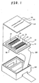
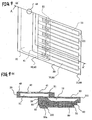
- Fig. 1 is a perspective arrangement view of the ink jet type recording head of Embodiment 1 of the present invention.
- Figs. 2(a) and (b) are cross-sectional views of the ink jet type recording head shown in Fig. 1.
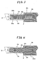
- Fig. 3 is a plan view showing the structure of the piezoelectric layer, upper electrode and lower electrode of the ink jet type recording head of Embodiment 1 of the present invention, wherein Fig. 3 is drawn in relation to the pressure generating chamber.
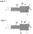
- Fig. 4 is a view showing a structure of the piezoelectric vibrator of one variation of Embodiment 1 of the present invention.
- Figs. 5(a) and (b) are views showing a structure of the piezoelectric vibrator of another variation of Embodiment 1 of the present invention.
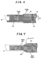
- Fig. 6 is a view showing a structure of the piezoelectric vibrator of still another variation of Embodiment 1 of the present invention.
- Fig. 7 is a view showing a structure of the piezoelectric vibrator of still another variation of Embodiment 1 of the present invention.
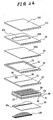
- Fig. 8 is an exploded perspective view of the ink jet type recording head of Embodiment 2 of the present invention.
- Figs. 9(a) and (b) are views of the ink jet type recording head of Embodiment 2 of the present invention, wherein Fig. 9(a) is a plan view and Fig. 9(b) is a cross-sectional view of Fig. 9(a) cut along A-A.
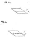
- Figs. 10(a) and (b) are views showing variations of the sealing plate shown in Fig. 8.
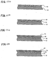
- Figs. 11(a)-(d) are views showing a thin film manufacturing process of Embodiment 2 of the present invention.
- Figs. 12(a)-(c) are views showing a thin film manufacturing process of Embodiment 2 of the present invention.
- Figs. 13(a)-(c) are views showing a thin film manufacturing process of Embodiment 2 of the present invention.
- Fig. 14 is a plan view of a primary portion of Embodiment 2 of the present invention.
- Fig. 15 is a plan view of a primary portion for explaining a variation of Embodiment 2 of the present invention.
- Fig. 16 is a plan view of a primary portion for explaining another variation of Embodiment 2 of the present invention.
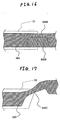
- Fig. 17 is a plan view of a primary portion for explaining still another variation of Embodiment 2 of the present invention.
- Fig. 18 is a plan view of a primary portion for explaining still another variation of Embodiment 2 of the present invention.
- Fig. 19 is a plan view of a primary portion for explaining still another variation of Embodiment 2 of the present invention.
- Fig. 20 is a plan view of a primary portion of Embodiment 3 of the present invention.
- Fig. 21 is a plan view of a primary portion for explaining a variation of Embodiment 3 of the present invention.
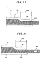
- Fig. 22 is a plan view of a primary portion for explaining Embodiment 4 of the present invention.
- Fig. 23 is a plan view of a primary portion for explaining a variation of Embodiment 4 of the present invention.
- Fig. 24 is a plan view of a primary portion for explaining another variation of Embodiment 4 of the present invention.
- Fig. 25 is a plan view of a primary portion for explaining still another variation of Embodiment 4 of the present invention.
- Fig. 26 is an exploded perspective view of the ink jet type recording head of another Embodiment of the present invention.
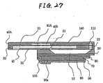
- Fig. 27 is across-sectional view of the ink jet type recording head of another Embodiment of the present invention.
- Fig. 1 is a perspective arrangement view of the ink jet type recording head of Embodiment 1 of the present invention.
- Figs. 2(a) and 2(b) are cross-sectional views respectively showing different sections of one pressure generating chamber taken in the longitudinal direction, that is, Fig. 2(a) is a cross-sectional view taken on the center line of the piezoelectric vibrator 310, and Fig. 2(b) is a cross-sectional view taken at the side end portion of the piezoelectric vibrator 310.
- Fig. 3 is a view showing a positional relation between them.
- a passage forming base pate 10 which is composed of a single crystal silicon base plate.
- One surface of the passage forming base pate 10 is an opening surface, and a piece of elastic film 50 made of silicon oxide is formed on the other surface.
- a pressure generating chamber 12 and a reservoir 13 which are formed by means of anisotropic etching and sectioned by bulkheads 11.
- an ink feed port 14 composed of a recess through which the pressure generating chamber 12 is communicated with the reservoir 13 at a constant flow resistance.
- a piezoelectric vibrator 310 which is made by the method of film formation, the details of which will be described later.
- nozzle plate 110 On the nozzle plate 110, there is formed a nozzle opening 111 through which the pressure generating chamber 12 is communicated at one end side.
- This nozzle plate 110 is fixed in such a manner that the opening of the passage forming base plate is covered with the nozzle plate 110.
- the passage forming base plate 10 is connected with a flexible cable 120 for supplying a drive signal to the piezoelectric vibrator 310.
- the passage forming base plate 10 is fixed to and held by a head case 130.
- the piezoelectric vibrator 310 is composed of a piezoelectric active section 320 which includes: a lower electrode film 60 provided on the elastic film 50 in such a manner that the lower electrode film 60 covers all regions of the pressure generating chamber 12, ink feed port 14 and reservoir 13; a piezoelectric layer 70 formed on this lower electrode film 60; and an upper electrode film 80, wherein these members are respectively laminated on each other.
- the piezoelectric active section 320 extends from the nozzle opening side of the pressure generating chamber 12 to the reservoir 13 side and exceeds the end portion of the reservoir 13.
- the width W2 of the piezoelectric active section 320 is essentially a little smaller than the width W1 of the pressure generating chamber 12, and the side edges 320a, 320a of the piezoelectric active section 320 are located inside the boundaries 12a, 12a between the pressure generating chamber 12 and the bulkheads 11.
- the width W3 of the piezoelectric active section 320 is larger than the width W1 of the pressure generating chamber 12, that is, the wide width section 321, the width of which is W3, is formed at the position P located inside of the boundary 12b of the end portion of the pressure generating chamber 12, and the piezoelectric active section 320 extends to a terminal section in which the piezoelectric active section 320 is connected with the flexible cable 120.
- the piezoelectric vibrator 310 when a signal is impressed upon the piezoelectric vibrator 310 from the outer drive circuit via the flexible cable 120, the piezoelectric vibrator 310 is deflected, so that the pressure generating chamber 12 is contracted.
- the pressure generating chamber 12 is contracted, ink in the pressure generating chamber 12 is pressurized. A portion of the thus pressurized ink is jetted from the nozzle opening 111 in the form of ink drops. After the ink drops have been jetted out from the nozzle opening 111 and the piezoelectric vibrator 310 has returned to the initial condition, the pressure generating chamber 12 is expanded, and ink flows from the reservoir 13 into the pressure generating chamber 12 via the ink feed port 14.
- the side edges 320a, 320a of the piezoelectric active section 320 are located inside of the boundaries 12a, 12a on the side of the pressure generating chamber 12. Accordingly, a restricting force given to the piezoelectric active section 320 by the passage forming base plate 10 is reduced as small as possible, so that the piezoelectric active section 320 is greatly deflected. Therefore, the piezoelectric active section 320 generates an ink pressure necessary for jetting ink even when a low drive voltage is impressed.
- the width W3 of the piezoelectric active section 320 is larger than the width W1 of the pressure generating chamber 12. Therefore, the deflecting displacement is restricted when the piezoelectric active section 320 is driven, and the concentration of stress is reduced.
- Fig. 4 is a view showing a variation of this embodiment.
- the upper electrode film 80 is not formed in a portion of the wide width section 321 in the above embodiment, but inactive sections 325, 325 are provided in which the piezoelectric layer 70 is exposed and the inactive sections 325, 325 become inert.
- the inactive sections 325, which are inert, are located outside of the width W2 of the primary portion of the piezoelectric active section 320 at the inner end portion of the pressure generating chamber 12 in the region where the width of the piezoelectric layer 70 is large.
- Other portions are the wide width section 321A of the piezoelectric active section 320.
- the lead section is formed in such a manner that the width of the wide width section 321 is determined to be W3.
- the lead section 85 of the width W4 which is determined to be as small as possible under the condition that a drive signal can not be attenuated, is formed on the upper electrode film 80, it is possible to ensure the creeping distance between the lower electrode film 60 and the upper electrode film 80, and the creeping discharge can be prevented, and at the same time, the electrostatic capacity of the signal feed passage and the piezoelectric loss can be remarkably reduced, and the deterioration of the response speed and the generation of heat can be suppressed.
- the vibrating plates arranged at least on both sides in the width direction of the primary portion of the piezoelectric active section 320 may be formed to be thin as compared with other portions so that the vibrating plates can be easily displaced in the case of driving.
- the lower electrode film removing sections 350 on both sides in the width direction of the piezoelectric active section 320. From the lower electrode film removing section 350, the lower electrode film 60 is completely removed.
- a thin film may be formed in such a manner that a portion of the lower electrode film 60 in the thickness direction is removed, or alternatively a portion of the elastic film 50 in the thickness direction may be removed.
- the lower electrode film removing section 350 may be arranged not only on both sides in the width direction but also outside of the edge portion.
- the width of the primary portion of the piezoelectric active section 320 may be gradually extended so that the width of the region can be gradually changed into the wide width section. That is, as shown in Fig. 7, the width of the wide width section 321B at the inside end portion with respect to the pressure generating chamber 12 is gradually changed so that it can be formed into the width changing section 322. Especially when the inner edge of a boundary between the primary section and the wide width section is formed into an R section, as shown in Fig. 7, it is possible to further reduce the occurrence of cracks in the inside edge section of the wide width section.
- Figs. 8 to 14 are views showing an ink jet type recording head related to Embodiment 2.
- the essential structure of this ink jet type recording head is similar to that of the embodiment described before except for one point that a common ink chamber is formed by a different member instead of the reservoir 13 arranged on the passage forming base plate 10. Therefore, like reference characters are used to indicate like parts.
- Fig. 8 is an exploded perspective arrangement view of the ink jet type recording head of an embodiment of the present invention.
- Fig. 9(a) is a plan view
- Fig. 9(b) is a cross-sectional view in the longitudinal direction of one of the pressure generating chambers.
- the passage forming base plate 10 is composed of a single crystal silicon base plate, the face orientation of which is (110). Thickness of the passage forming base plate 10 is usually 150 to 300 ⁇ m. It is preferable that the thickness of the passage forming base plate 10 is 180 to 280 ⁇ m. It Is more preferable that the thickness of the passage forming base plate 10 is approximately 220 ⁇ m. The reason why the thickness of the passage forming base plate 10 is determined as described above is that the arranging density of the pressure chambers can be increased while the rigidity of the bulkhead between the adjoining pressure generating chambers is maintained high.
- One of the surfaces of the passage forming base plate 10 is an opening surface, and on the other surface, there is provided an elastic film 50, the thickness of which is 0.1 to 2 ⁇ m, made of silicon dioxide previously formed by means of heat oxidation.
- a nozzle opening 111 and a pressure generating chamber 12 which are formed by conducting anisotropic etching on a single crystal silicon base plate.
- the anisotropic etching is conducted in the following manner.
- an alkali solution such as a solution of KOH
- the first face (111) appears, which is perpendicular to the face (110)
- the second face (111) appears which forms an angle of about 70° with the first face (111) and also forms an angle of about 35° with the above face (110).
- the characteristic is used in which the etching rate of the face (111) is approximately 1/180 with respect to the etching rate of the face (110).
- a shape of a parallelogram which is formed by the first faces (111), the number of which is two, and the second faces (111), the number of which is two, which are inclined with respect to the first faces.
- the pressure generating chambers 12 can be arranged at a high arrangement density.
- each pressure generating chamber 12 is formed by the first face (111), and the short side is formed by the second face (111).
- This pressure generating chamber 12 can be formed when etching is conducted on the passage forming base plate 10 in such a manner that the etched portion substantially penetrates the passage forming base plate 10 so that it can reach the elastic film 50.
- the elastic film 50 is seldom corroded by the alkali solution used for etching the single crystal silicon base plate.
- each nozzle opening 111 communicated with one end of each pressure generating chamber 12 is smaller than the width of the pressure generating chamber 12.
- the depth of each nozzle opening 111 is smaller than the depth of the pressure generating chamber 12. That is, the nozzle opening 111 is formed when the single crystal silicon base plate is etched in the thickness direction to the middle of the thickness. That is, the nozzle opening 111 is formed when half-etching is conducted on the single crystal silicon base plate. In this connection, half-etching is conducted by adjusting the etching time.
- the size of the pressure generating chamber 12 which generates pressure for jetting ink drops and the size of the nozzle opening 111 from which ink drops are jetted out are optimized in accordance with a quantity of ink to be jetted out, jetting speed of ink drops and jetting frequency. For example, when ink drops, the number of which is 360 per inch, are recorded, it is necessary to form the nozzle opening 111 with high accuracy, the groove width of which is several tens ⁇ m.
- Each pressure generating chamber 12 and the common ink chamber 31, which will be described later, are communicated with each other via the ink feed communicating port 21 formed at a position on a sealing plate 20 corresponding to one end portion of each pressure generating chamber 12. Ink is fed from the common ink chamber 31 via this ink feed communicating port 21 and distributed to each pressure generating chamber 12.
- the sealing plate 20 On the sealing plate 20, there are formed ink feed communicating ports 21 corresponding to the pressure generating chambers 12.
- the sealing plate 20 is made of glass ceramic, the thickness of which is 0.1 to 1 mm and the coefficient of linear expansion of which is 2.5 to 4.5 (10 -6 /°C).
- the ink feed communicating port 21 may be one slit-shaped hole 21A which crosses a portion close to the end portion of each pressure generating chamber 12 on the ink feed side, or alternatively the ink feed communicating port 21 may be a plurality of slit-shaped holes 21B.
- One surface of the sealing plate 20 covers the overall surface of the passage forming base plate 10, so that the sealing plate 20 functions as a protective plate for protecting the single crystal silicon base plate from a force given from the outside of the recording head. Also, the other surface of the sealing plate 20 composes a wall surface of the common ink chamber 31.
- the common ink chamber forming base plate 30 composes a circumferential wall of the common ink chamber 31.
- the thickness of the common ink chamber forming base plate 30 is determined in accordance with the number of nozzle openings and the ink drop jetting frequency.
- This common ink chamber forming base plate 30 is made by punching a stainless steel plate of appropriate thickness. In this embodiment, the thickness of the common ink chamber forming base plate 30 is 0.2 mm.
- the ink chamber side plate 40 is composed of a stainless steel base plate. One surface of the ink chamber side plate 40 composes a wall surface of the common ink chamber 31. On the other surface of the ink chamber side plate 40, half-etching is conducted, so that a recess portion 40a is formed. In this way, a thin wall 41 is formed on the other surface of the ink chamber side plate 40. On the ink chamber side plate 40, there is formed an ink introducing port 42 by means of punching through which ink is supplied from the outside of the recording head. In this connection, the thin wall 41 is provided for absorbing pressure directed to the side opposite to the nozzle opening 111 which is generated in the case of jetting ink.
- the thin wall 41 prevents an unnecessary positive or negative pressure from being given to other pressure generating chambers 12 via the common ink chamber 31.
- consideration is given to the rigidity necessary for connecting the ink introducing port 42 with the ink supply means provided outside the recording head, and the thickness of the ink chamber side plate 40 is determined to be 0.2 mm, and one portion of the ink chamber side plate 40 is determined to be 0.02 mm so as to form a thin wall 41.
- the thickness of the ink chamber side wall 40 may be determined to be 0.02 mm at the beginning.
- a lower electrode film 60 the thickness of which is approximately 0.5 ⁇ m
- a piezoelectric film 70 the thickness of which is approximately 1 ⁇ m
- an upper electrode film 80 the thickness of which is approximately 0.1 ⁇ m, which are laminated on each other in the process described later.
- the piezoelectric vibrator piezoelectric element
- a region on this elastic film 50 opposed to each pressure generating chamber 12 there is provided an independent piezoelectric vibrator for each pressure generating chamber 12.
- the lower electrode film 60 functions as a common electrode of the piezoelectric vibrators
- the upper electrode film 80 functions as an individual electrode of the piezoelectric vibrator.
- the piezoelectric film 70 is individually provided corresponding to each pressure generating chamber 12.
- the piezoelectric film 70 may be provided on the overall surface
- the upper electrode film 80 may be individually provided corresponding to each pressure generating chamber 12. In any case described above, the piezoelectric active section is formed for each pressure generating chamber 12.
- a wafer made of a single crystal silicon base plate which is formed into a passage forming base plate 10.
- This wafer is thermally oxidized at 1100°C in a diffusion furnace, so that an elastic film 50 of silicon dioxide is formed.
- the lower electrode film 60 is formed by means of spattering.
- Pt is preferably used.
- the reason why Pt is used for the material of the lower electrode film 60 is described as follows.
- the piezoelectric film 70 described later which is formed by the process of spattering or the process of sol-gel, must be fired after the formation of film at the temperature of 600 to 1000°C in the atmosphere or oxygen gas, so that the piezoelectric film 70 can be crystallized. That is, the material of the lower electrode film 70 must be electrically conductive in the oxidizing atmosphere of high temperature described above.
- PZT is used for the piezoelectric film 70, it is preferable that the conductivity is seldom changed by the diffusion of PbO.
- Pt is preferably used.
- the piezoelectric film 70 is formed as shown in Fig. 11(c).
- the process of sol-gel is used.
- sol in which a metallic organic matter is dissolved and dispersed in solvent is coated and dried, so that sol is changed into gel, and the thus obtained gel is fired at high temperature.
- the piezoelectric film 70 made of metallic oxide is obtained.
- the piezoelectric film 70 is used for an ink jet type recording head, it is preferably made of lead zirconate titanate (PZT).
- the upper electrode film 80 is formed.
- any material may be used for the upper electrode film 80.
- Metal such as Al, Au, Ni or Pt can be used, and also electrically conductive oxide can be used.
- the upper electrode film 80 is made of Pt by the process of spattering.
- the lower electrode film 60, piezoelectric film 70 and upper electrode film 80 are etched all together so that the overall pattern of the lower electrode 60 is formed.
- Fig. 12(b) when only the piezoelectric film 70 and the upper electrode film 80 are etched, so that patterning can be conducted on the piezoelectric active section 320.
- Fig. 12(c) a portion of the lower electrode 60 corresponding to an arm of the vibrating plate on both sides of the piezoelectric active section 320 is removed, wherein this portion is opposed to both sides in the width direction of each pressure generating chamber 12.
- the pressure generating chamber 12 has not been formed yet, it is shown by a broken line in Fig. 12. Due to the foregoing, the lower electrode film removing section 350 is formed. When the lower electrode film removing section 350 is formed in this way, an amount of displacement caused by impressing voltage upon the piezoelectric active section 320 can be increased.
- the entire lower electrode film 60 is not necessarily removed from the lower electrode film removing section 350, but the thickness of the lower electrode film may be reduced.
- the lower electrode film removing section 350 is formed in the portion corresponding to the am section of the piezoelectric active section 320 in this embodiment.
- the present invention is not limited to the above specific embodiment.
- the lower electrode film removing section 350 may be formed in a portion outside of both end portions in the longitudinal direction of the piezoelectric active section 320. Alternatively, it may be formed in the substantial overall peripheral edge portion of the pressure generating chamber. Of course, this lower electrode removing section 350 is not necessarily provided.
- an insulating layer 90 having an electrically insulating property is formed in such a manner that it covers at least the circumferential edge of the upper surface of each upper electrode film 80 and also covers the sides of the piezoelectric film 70 and the lower electrode film 60 (shown in Fig. 8).
- the insulating layer 90 is made of material from which a film can be formed by the film forming method or the etching method. Examples of the material of the insulating layer 90 are: silicon oxide, silicon nitride, and organic material. It is preferable that the insulating layer 90 is made of photosensitive polyimide, the rigidity of which is low and the electric insulating property of which is excellent.
- each piezoelectric active section 320 there are formed contact holes 90a through which a portion of the upper electrode film 80 is exposed so that it can be connected with the lead electrode 100 described later.
- One end of the lead electrode 100 is connected with each upper electrode film 80 via this contact hole 90a, and the other end of the lead electrode 100 is connected with the connecting terminal section.
- the width of the lead electrode 100 is formed to be as narrow as possible so that a drive signal can be positively fed to the upper electrode film 80.
- Figs. 13(a) to 13(c) are views showing a forming process of the above insulating layer.
- the insulating layer 90 is formed by the following film forming process, so that the insulating layer 90 can cover the circumferential edge of the upper electrode layer 80 and the sides of the piezoelectric film 70 and the lower electrode film 60.
- Preferable materials of this insulating layer 90 are described above.
- a negative type photosensitive polyimide is used.
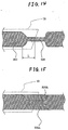
- Fig. 13(b) shows a cross-section of the contact hole 90a in a region opposed to the outer circumferential wall of the pressure generating chamber 12.
- the contact hole 90a connects the lead electrode 100 with the upper electrode film 80.
- the upper electrode film 80 may be extended to an end portion of the base plate, and it may be directly connected with a flexible cable.
- the contact hole 90a may be provided in a region opposed to the pressure generating chamber 12.
- anisotropic etching is conducted on the single crystal silicon base plate in the alkali solution described before, so that the pressure generating chamber 12 and others can be formed.
- a large number of chips are simultaneously formed on one wafer.
- the passage forming base plate 10 of one chip size is divided as shown in Fig. 8. The thus divided passage forming base plate 10 is successively made to adhere onto the sealing plate 20, common ink chamber forming base plate 30 and ink chamber side plate 40, so that these plates can be integrated into one body. In this way, the ink jet type recording head can be formed.
- Ink drops are jetted out from the thus composed ink jet head as follows. Ink is fed from the ink introducing port 42 connected with an outside ink feed means not illustrated in the drawing. Members from the common ink chamber 31 to the nozzle opening 111 are filled with ink. After that, according to a recording signal sent from a drive circuit not shown in the drawing and provided outside, voltage is impressed between the lower electrode film 60 and the upper electrode film 80 via the lead electrode 100, so that the elastic film 50, lower electrode film 60 and piezoelectric film 70 are deflected. Due to the above deflection, pressure in the pressure generating chamber 12 can be increased and ink drops can be jetted out from the nozzle opening 111.
- Fig. 14 is a view showing a positional relationship between the pressure generating chamber 12 and the piezoelectric active section 320 of the thus formed ink jet type recording head.
- the piezoelectric active section 320 composed of the piezoelectric film 70 and the upper electrode film 80 is essentially arranged in a region opposed to the pressure generating chamber 12, and the width of the piezoelectric active section 320 is a little smaller than the width of the pressure generating chamber 12.
- the piezoelectric active section 320 continuously extends through a narrow width section 323 which is arranged in a portion close to the connecting section crossing from a region opposed to the pressure generating chamber 12 to a region opposed to the circumferential wall.
- the width of the narrow width section 323 located in a portion close to the boundary between the pressure generating chamber 12 and the circumferential wall is smaller than the widths of other portions.
- the narrow width section 323 of this embodiment is formed in such a manner that widths of both the piezoelectric film 70 and the upper electrode film 80 are reduced.
- the width of the pressure generating chamber 12 is 50 ⁇ m
- the width of the piezoelectric active section 320 is 35 to 40 ⁇ m
- the width the piezoelectric layer 70 of the narrow width section 323 is 10 to 15 ⁇ m.
- a distance L from an end portion of the narrow width section 323 on the pressure generating chamber 12 side, that is, from a position at which the width of the piezoelectric active section 320 starts decreasing, to a position at which the narrow width section 323 crosses a boundary of the circumferential wall is preferably not less than 1/2 of the width of the pressure generating chamber 12.
- Fig. 15 is a view showing a pattern of the piezoelectric active section close to the pressure generating chamber of the ink jet type recording head of a variation of Embodiment 2.
- the narrow width section 323A of the piezoelectric active section 320 is formed when the width of the upper electrode film 80 is reduced, and an inactive section (inert section) 325A composed of the piezoelectric film 70 having no upper electrode film 80 is provided on both sides of the narrow width section 323A.
- inactive section inactive section
- deflection caused in the narrow width section 323A can be suppressed, so that damage caused by cracks can be prevented and the durability can be enhanced.
- Fig. 16 is a view showing a pattern of the piezoelectric active section close to the pressure generating chamber of the ink jet type recording head of another variation of Embodiment 2.
- the narrow width section 323B is formed in such a manner that the width of the piezoelectric active section 320 is reduced when it is biased onto one side wall of the pressure generating chamber 12. Due to the above arrangement, when voltage is impressed, the deflection of the narrow width section 323B at the end of the pressure generating chamber 12 becomes smaller than the deflection in the case where the connecting section is located at the center. In the narrow width section 323B, only the width of the upper electrode film 80 is reduced, and the inactive section 325B is provided on one side of the narrow width section 323B. Of course, the piezoelectric film 70 of the inactive section 325B may be removed.
- Fig. 17 is a view showing a pattern of the piezoelectric active section close to the pressure generating chamber of the ink jet type recording head of still another variation of Embodiment 2.
- the narrow width section 323C is formed in such a manner that the piezoelectric active section 320 crosses the corner of the pressure generating chamber 12. Due to the above arrangement, when voltage is impressed, the deflection of the narrow width section 323C at the end of the pressure generating chamber 12 becomes smaller than the deflection in the case where the connecting section is located at the edge. In the narrow width section 323C, the widths of the upper electrode film 80 and the piezoelectric film 70 are reduced.
- Fig. 18 is a view showing a pattern of the piezoelectric active section close to the pressure generating chamber of the ink jet type recording head of still another variation of Embodiment 2.
- two narrow width sections 323D are arranged in the regions opposed to two corner portions of the pressure generating chamber 12. Other points are the same as those of the embodiment shown in Fig. 17. Accordingly, the piezoelectric film 70 and the upper electrode film 80 are removed from between the two narrow width sections 323D. In this connection, the effects of this embodiment are substantially the same as those of the embodiment shown in Fig. 17.
- Fig. 19 is a view showing a pattern of the piezoelectric active section close to the pressure generating chamber of the ink jet type recording head of still another variation of Embodiment 2.
- the narrow width sections 323E are arranged in portions opposed to each other close to the two corner portions of the pressure generating chamber 12. Other points are the same as those of the embodiment shown in Fig. 16. Accordingly, the piezoelectric film 70 and the upper electrode film 80 are removed from between the narrow width sections 323E. In this connection, the effects of this embodiment are substantially the same as those of the embodiment shown in Fig. 16. In this connection, when the contact hole 90a is not formed in a region opposed to the pressure generating chamber 12, but it is formed outside the region. Therefore, it is possible to prevent the occurrence of cracks in a portion close to the contact hole 90a.
- Fig. 20 is a plan view showing a primary portion of the ink jet type recording head of Embodiment 3.
- the essential structure of the ink jet type recording head of this embodiment is the same as that of Embodiment 2. Therefore, like reference characters are used to indicate like parts.
- the piezoelectric active section 320 is essentially located in a region opposed to the pressure generating chamber 12, and the lower electrode removing section 350 is formed in its periphery.
- the piezoelectric active section 320 is extended via the narrow width section 323F to a region opposed to the circumferential wall at the end portion in the longitudinal direction of the pressure generating chamber 12.
- thick film sections 360 on both sides of the narrow width section 323F in the width direction in this embodiment.
- the thick film sections 360 are regions arranged on both sides of the narrow width section 323F in the width direction and opposed to the inside of the boundary between the pressure generating chamber 12 and the circumferential wall.
- the thick film section 360 may be thicker than the lower electrode film removing section 350.
- the thick film section 360 is formed when the lower electrode film 60 is not removed. That is, the thick film section 360 is formed when the lower electrode film 60 is left as it is. Further, when the thick film section 360 is formed, the piezoelectric film 70 and the upper electrode film 80 may be left as they are. Furthermore, the insulating layer and other layers may be laminated.
- the displacement caused by the deflection of the narrow width section 323F is further restricted when it is driven.
- a portion of the vibrating plate opposed to the inside of the boundary between the pressure generating chamber 12 and the circumferential wall is protected by the thick film section 360. Therefore, the durability of the vibrating plate can be enhanced.
- Fig. 21 is a view showing a variation of Embodiment 3.
- the narrow width section 323G is formed in such a manner that it crosses a region opposed to one corner of the pressure generating chamber 12.
- the thick film section 360A is arranged on the inside of the boundary of the other corner of the pressure generating chamber 12. Therefore, the same effect can be provided.
- Fig. 22 is a view showing a pattern of the piezoelectric active section arranged close to the pressure generating chamber of the ink jet type recording head of Embodiment 4 of the present invention.
- the essential structure of this embodiment is the same as that of Embodiment 2, and like reference characters are used to indicate like parts.
- a narrow width section 380 at one end portion of the pressure generating chamber 12 corresponding to the narrow width section 323H of the piezoelectric active section 320.
- This narrow width section 380 is a vibration restricting section 370A.
- the piezoelectric active section 320 is extended from an end portion corresponding to the vibration restricting section 370A to the circumferential wall.
- the occurrence of cracks can be prevented and the durability can be enhanced as follows.
- the piezoelectric active section 320 is formed into the narrow width section 323H as described above. Therefore, the displacement is restricted in the case of driving, and further when the width of the pressure generating chamber 12 is reduced, the displacement can be further restricted. Therefore, the displacement can be reduced to be smaller than the displacement of other sections, and the deflection is gradually caused from the circumferential wall boundary toward the pressure generating chamber 12. Therefore, an intensity of stress in the piezoelectric active section 320 located in the vibration restricting section 370A is decreased. Accordingly, the occurrence of cracks can be prevented and the durability can be enhanced.
- the width of the piezoelectric active section 320 in the narrow width section 380 is reduced.
- the width of the piezoelectric active section 320 is not necessarily reduced.
- the lower electrode removing section may be arranged.
- the lower electrode removing section may be arranged in the entire sections including the vibration restricting section. Otherwise, the lower electrode removing section may be arranged in the sections except for the vibration restricting section.
- the contact hole is formed at a position opposed to the pressure generating chamber 12.
- Fig. 23 is a view showing a pattern of the piezoelectric active section arranged close to the pressure generating chamber of the ink jet type recording head of a variation of Embodiment 4.
- the contact hole 90a is formed in a portion opposed to the circumferential wall of the pressure generating chamber 12, and other points are the same as those of the embodiment described above. In this case, no substantial displacement is caused in the periphery of the contact hole 90a. Therefore, cracks are seldom caused in this portion.
- Fig. 24 is a view showing a pattern of the piezoelectric active section arranged close to the pressure generating chamber of the ink jet type recording head of a variation of Embodiment 4.
- a narrow width section 380A at one end portion of the pressure generating chamber 12, and a portion of the piezoelectric active section 320 corresponding to the narrow width section 380A is made to be a wide width section 321C so that it can be formed into a vibration restricting section 370B.
- the displacement of this portion is smaller than that of other portions, and the deflection is gradually caused from the circumferential wall boundary to the pressure generating chamber 12. Accordingly, an intensity of stress of the piezoelectric active section 320 located in the vibration restricting section 370B is decreased. Therefore, the occurrence of cracks can be prevented and the durability can be enhanced.
- the narrow width section 380A of the pressure generating chamber 12 is formed in such a manner that the width is gradually reduced from both sides in the width direction so that the edge profile is formed into a curve.
- the wide width section 321C of the piezoelectric active section 320 is formed in such a manner that the width of the piezoelectric active section 320 is gradually extended onto both sides in the width direction. Due to the foregoing, the number of corners of the piezoelectric film 70 in which cracks tend to occur can be suppressed. Accordingly, the durability can be further enhanced.
- Fig. 25 is a view showing a pattern of the piezoelectric active section arranged close to the pressure generating chamber of the ink jet type recording head of a variation of Embodiment 4.
- the narrow width section 380B is arranged in portions except for the end portion of the pressure generating chamber 12 in the longitudinal direction, so that the narrow width section 380B can become a vibration restricting section 370C.
- Other points are the same as those of the embodiment described before.
- the narrow width section 323I of the piezoelectric active section 320 is formed on the side circumferential wall of the pressure generating chamber 12, and the contact hole 90a is formed in the narrow width section 323I.
- the connecting section of the piezoelectric active section 320 extending in the width direction of the pressure generating chamber 12 is not limited to a case in which the vibration restricting section is arranged in a portion except for the end portion of the pressure generating chambers 12. Even in a case in which the vibration restricting section is arranged in the end portion like each embodiment described above, the connecting section extending to the side may be arranged.
- the sealing plate 20 described before may be made of glass ceramic.
- the thin film (wall) 41 may be a different member and made of glass ceramic, that is, the material and structure may be freely changed.
- the nozzle opening is formed on an end surface of the passage forming base plate 10, however, it is possible to provide a nozzle opening protruding in a direction perpendicular to the surface.
- Fig. 26 is an exploded perspective view of the embodiment composed as described above.
- Fig. 27 is a cross-sectional view of the passage.
- the nozzle openings 111 are formed on the nozzle base plate 140 opposite to the piezoelectric vibrator.
- the nozzle communicating ports 22 to communicate these nozzle openings 111 with the pressure generating chambers 12 are formed penetrating the sealing plate 20, common ink chamber forming plate 30, thin plate 41A and ink chamber side plate 40A.
- the thin plate 41A and the ink chamber side plate 40A are made to be different members, and the opening 40b is formed on the ink chamber side plate 40.
- Other points are essentially the same as those of the embodiments described before.
- Like reference characters are used to indicate like parts, and the same explanations are omitted here.
- the present invention can be applied to an ink jet type recording head in which the common ink chamber is formed on the passage forming base plate.
- the present invention is applied to an ink jet type recording head of thin film type manufactured by the process of film formation or the process of lithography.
- the present invention is not limited to the above specific embodiment.
- the present invention can be applied to various types of ink jet recording heads such as an ink jet recording head in which the base plates are laminated so as to form pressure chambers, an ink jet recording head in which the piezoelectric film is formed by the process of adhering green sheets or the process of screen printing, and an ink jet recording head in which the piezoelectric film is formed by the growth of crystals.
- the vibrating plate is composed of an elastic film which is provided differently from the lower electrode film.
- the lower electrode film may be also used as an elastic film.
- an insulating layer between the piezoelectric vibrator and the lead electrode.
- the present invention is not limited to the above specific embodiment.
- the following arrangements may be adopted.
- connection may be conducted by using various bonding technique such as wire bonding.
- the upper electrode film 80 is made of Pt.
- the piezoelectric layer 70 is made of PZT, it is preferable to use electrically conductive oxide instead of Pt.
- Pt takes oxygen from PZT, so that the piezoelectric characteristic is deteriorated when oxygen is absorbed by Pt.
- electrically conductive oxide material may be used.
- Examples of usable conductive oxide materials are: TiO, Ti 2 O 3 , Ti 3 O 5 , Ti 4 O 7 , Ti 5 O 9 , Ti 6 O 11 , Ti 7 O 13 , Ti 8 O 15 , Ti 9 O 17 , VO, VO 2 , V 2 O 3 , V 3 O 5 , V 4 O 7 , V 5 O 9 , V 6 O 11 , V 7 O 13 , V 8 O 15 , SnO 2-x wherein 0 ⁇ x ⁇ 2 in the above composition formula, NbO, NbO 2 , LaO, SmO, NdO, Fe 3 O 4 , ReO 3 , ReO 2 , Rh 2 O 3 , RhO 2 , CrO 2 , MoO 2 , WO 2 , RuO 2 , OsO 2 , IrO 2 , PtO 2 , LiTi 2 O 4 , LiV 2 O 4 , K 2 P 8 W 32 O 112 , Rb 2 P 8 W 32 O 11
- Examples of usable conductive materials are Ir, Pd, Rb and Ru.
- the layer of IrO x , PdO x , RbO x or RuO x is formed on the piezoelectric layer 70 and the interface, and the same effect can be provided.
- the conductive film of Pt may be laminated on the layer made of the above materials so as to form an upper electrode film 80.
- a vibration regulating section in which vibration caused by the impression of voltage is relatively regulated, and the piezoelectric active section is extended onto the circumferential wall by this vibration regulating section. Therefore, deflection in this portion can be reduced as compared with that of other portions. Accordingly, the occurrence of cracks can be prevented and the durability can be enhanced.
Abstract
Description
Claims (24)
- An ink jet type recording head comprising:a piezoelectric vibrator including:a vibrating plate composing a portion of a pressure generating chamber communicated with a nozzle opening, an upper surface of the vibrating plate functioning as a lower electrode;a piezoelectric active section composed of a piezoelectric layer, formed on the upper surface of the vibrating plate;an upper electrode formed on the surface of the piezoelectric layer, the piezoelectric active section being formed in a region opposed to the pressure generating chamber;
wherein the piezoelectric active section is essentially arranged in a region opposed to the pressure generating chamber, the piezoelectric active section has a connecting section that crosses a boundary between the region opposed to the pressure generating chamber and a region opposed to a circumferential wall at least in one portion; and
wherein the piezoelectric active section has a vibration regulating section for regulating a vibrating movement of the vibrating plate. - An ink jet type recording head according to claim 1, wherein the vibrating plate has a thin wall section, a thickness of which is thinner than a thickness of a portion corresponding to the piezoelectric active section, on both sides of the piezoelectric active section in a width direction.
- An ink jet type recording head according to claim 1, wherein the vibration regulating section is composed of a wide width section in which the piezoelectric layers is wider than a primary portion of the piezoelectric active section, and the wide width section is extended to a side wall and arranged on one end side of the pressure generating chamber in a longitudinal direction.
- An ink jet type recording head according to claim 3, wherein the upper electrode is essentially arranged on the piezoelectric layer of the vibration regulating section.
- An ink jet type recording head according to claim 3, wherein the upper electrode is not arranged at least on one portion of the piezoelectric layer of the vibration regulating section.
- An ink jet type recording head according to claim 3, wherein a width of the piezoelectric layer is gradually changed from the primary portion of the piezoelectric active section to the wide width section.
- An ink jet type recording head according to claim 1, wherein the vibration regulating section is formed by changing a relative relation between a width of the pressure generating section and a width of the piezoelectric active section from a relative relation of the primary portion.
- An ink jet type recording head according to claim 7, wherein the vibrating regulating section is composed of a narrow width section in which both the width of the piezoelectric layer close to the connecting section and a width of the upper electrode are reduced.
- An ink jet type recording head according to claim 7, wherein the vibration regulating section is composed of a narrow width section in which only a width of the upper electrode of the piezoelectric active section close to the connecting section is reduced.
- An ink jet type recording head according to claim 7, wherein the width of the piezoelectric active section is gradually changed from the primary section to the narrow width section.
- An ink jet type recording head according to claim 8, wherein a thick film section, an entire film thickness of which is larger than an entire film thickness in a periphery of the piezoelectric active section, is arranged at least in a portion of an inner edge of the boundary between the pressure generating chamber and the circumferential wall on both sides of the narrow width section in the width direction.
- An ink jet type recording head according to claim 8, wherein a distance from an end of the narrow width section inside the pressure generating chamber to a position at which the narrow width section crosses the boundary of one of the end portions of the pressure generating chamber in the longitudinal direction, is not less than 1/2 of the width of the pressure generating chamber.
- An ink jet type recording head according to claim 8, wherein the connecting section is arranged at a position close to either side wall of the pressure generating chamber.
- An ink jet type recording head according to claim 12, wherein a plurality of connecting sections are provided at one end portion of the pressure generating chamber in the longitudinal direction.
- An ink jet type recording head according to claim 14, wherein the connecting section is arranged so that it crosses a boundary at a corner of the pressure generating chamber.
- An ink jet type recording head according to claim 15, wherein an opening angle of the corner toward the pressure chamber is an acute angle.
- An ink jet type recording head according to claim 16, wherein the vibration regulating section is formed when the width of the pressure generating chamber is reduced to be smaller than widths of other portions.
- An ink jet type recording head according to claim 17, wherein a boundary between one side of the pressure generating chamber in the width direction and the circumferential wall is formed to be linear from the vibration regulating section to other portions.
- An ink jet type recording head according to claim 18, wherein an edge portion of the piezoelectric active section on one side in the width direction is formed to be linear in the longitudinal direction of the pressure generating chamber from the primary section to the vibration regulating section.
- An ink jet type recording head according to claim 19, wherein an insulating layer is formed on the upper surface of the piezoelectric active section, and a lead electrode used for impressing voltage on the piezoelectric active section and a contact section for connecting the electrode are arranged in a contact hole formed on the insulating layer.
- An ink jet type recording head according to claim 20, wherein the lead electrode used for impressing voltage on the piezoelectric active section and the contact section for connecting the electrode are arranged in a portion opposed to the circumferential wall of the pressure generating chamber.
- An ink jet type recording head according to claim 1, wherein a signal transmitting passage is formed when the width of the upper electrode is reduced from a region exceeding the boundary of the connecting section on one side of the pressure generating chamber.
- An ink jet type recording head according to claim 1, wherein at least a contact surface of the upper electrode coming into contact with the piezoelectric layer is made of conductive oxide film.
- An ink jet type recording head according to claim 1, wherein the pressure generating chamber is formed when anisotropic etching is conducted on a single crystal silicon base plate and each layer of the piezoelectric vibrator is formed by methods of film formation and lithography.
Applications Claiming Priority (12)
| Application Number | Priority Date | Filing Date | Title |
|---|---|---|---|
| JP2607497 | 1997-01-24 | ||
| JP26074/97 | 1997-01-24 | ||
| JP2607497 | 1997-01-24 | ||
| JP25221597 | 1997-09-17 | ||
| JP252215/97 | 1997-09-17 | ||
| JP25221597 | 1997-09-17 | ||
| JP25552297 | 1997-09-19 | ||
| JP255522/97 | 1997-09-19 | ||
| JP25552297 | 1997-09-19 | ||
| JP33277997 | 1997-12-03 | ||
| JP332779/97 | 1997-12-03 | ||
| JP33277997A JP3414227B2 (en) | 1997-01-24 | 1997-12-03 | Ink jet recording head |
Publications (3)
| Publication Number | Publication Date |
|---|---|
| EP0855273A2 true EP0855273A2 (en) | 1998-07-29 |
| EP0855273A3 EP0855273A3 (en) | 1999-08-18 |
| EP0855273B1 EP0855273B1 (en) | 2002-12-04 |
Family
ID=27458425
Family Applications (1)
| Application Number | Title | Priority Date | Filing Date |
|---|---|---|---|
| EP98101182A Expired - Lifetime EP0855273B1 (en) | 1997-01-24 | 1998-01-23 | Ink jet type recording head |
Country Status (4)
| Country | Link |
|---|---|
| US (1) | US6113225A (en) |
| EP (1) | EP0855273B1 (en) |
| JP (1) | JP3414227B2 (en) |
| DE (1) | DE69809807T2 (en) |
Cited By (4)
| Publication number | Priority date | Publication date | Assignee | Title |
|---|---|---|---|---|
| EP0895863A2 (en) * | 1997-07-31 | 1999-02-10 | Seiko Epson Corporation | Ink jet recording head |
| EP1013429A2 (en) * | 1998-12-25 | 2000-06-28 | Fujitsu Limited | Ink jet printer head and printer apparatus |
| WO2001025018A3 (en) * | 1999-10-05 | 2001-12-06 | Spectra Inc | Piezoelectric ink jet module with seal |
| EP1953839A1 (en) * | 2007-01-30 | 2008-08-06 | Matsushita Electric Industrial Co., Ltd. | Piezoelectric Element, Ink Jet Head, and Ink Jet Recording Device |
Families Citing this family (34)
| Publication number | Priority date | Publication date | Assignee | Title |
|---|---|---|---|---|
| US6502928B1 (en) * | 1998-07-29 | 2003-01-07 | Seiko Epson Corporation | Ink jet recording head and ink jet recording apparatus comprising the same |
| US6774541B1 (en) * | 1999-11-18 | 2004-08-10 | Kri, Inc. | Piezoelectric element, process for producing the piezoelectric element, and head for ink-jet printer using the piezoelectric element |
| US6693033B2 (en) * | 2000-02-10 | 2004-02-17 | Motorola, Inc. | Method of removing an amorphous oxide from a monocrystalline surface |
| JP2002001955A (en) * | 2000-06-26 | 2002-01-08 | Toshiba Tec Corp | Ink jet printer head and its manufacturing method |
| JP2002248765A (en) * | 2000-12-19 | 2002-09-03 | Fuji Xerox Co Ltd | Ink-jet recording head and ink-jet recording apparatus |
| US20020096683A1 (en) * | 2001-01-19 | 2002-07-25 | Motorola, Inc. | Structure and method for fabricating GaN devices utilizing the formation of a compliant substrate |
| US6709989B2 (en) | 2001-06-21 | 2004-03-23 | Motorola, Inc. | Method for fabricating a semiconductor structure including a metal oxide interface with silicon |
| US7019332B2 (en) * | 2001-07-20 | 2006-03-28 | Freescale Semiconductor, Inc. | Fabrication of a wavelength locker within a semiconductor structure |
| US6693298B2 (en) | 2001-07-20 | 2004-02-17 | Motorola, Inc. | Structure and method for fabricating epitaxial semiconductor on insulator (SOI) structures and devices utilizing the formation of a compliant substrate for materials used to form same |
| US6639249B2 (en) * | 2001-08-06 | 2003-10-28 | Motorola, Inc. | Structure and method for fabrication for a solid-state lighting device |
| US20030026310A1 (en) * | 2001-08-06 | 2003-02-06 | Motorola, Inc. | Structure and method for fabrication for a lighting device |
| US6673667B2 (en) * | 2001-08-15 | 2004-01-06 | Motorola, Inc. | Method for manufacturing a substantially integral monolithic apparatus including a plurality of semiconductor materials |
| US6911155B2 (en) * | 2002-01-31 | 2005-06-28 | Hewlett-Packard Development Company, L.P. | Methods and systems for forming slots in a substrate |
| US20030140496A1 (en) * | 2002-01-31 | 2003-07-31 | Shen Buswell | Methods and systems for forming slots in a semiconductor substrate |
| US7051426B2 (en) * | 2002-01-31 | 2006-05-30 | Hewlett-Packard Development Company, L.P. | Method making a cutting disk into of a substrate |
| JP4708667B2 (en) * | 2002-08-08 | 2011-06-22 | キヤノン株式会社 | Actuator and liquid jet head |
| JP2004114558A (en) * | 2002-09-27 | 2004-04-15 | Brother Ind Ltd | Inkjet printer head and manufacturing method therefor |
| US7169619B2 (en) * | 2002-11-19 | 2007-01-30 | Freescale Semiconductor, Inc. | Method for fabricating semiconductor structures on vicinal substrates using a low temperature, low pressure, alkaline earth metal-rich process |
| US6806202B2 (en) | 2002-12-03 | 2004-10-19 | Motorola, Inc. | Method of removing silicon oxide from a surface of a substrate |
| US6963090B2 (en) * | 2003-01-09 | 2005-11-08 | Freescale Semiconductor, Inc. | Enhancement mode metal-oxide-semiconductor field effect transistor |
| US20050036004A1 (en) * | 2003-08-13 | 2005-02-17 | Barbara Horn | Methods and systems for conditioning slotted substrates |
| KR100528350B1 (en) * | 2004-02-27 | 2005-11-15 | 삼성전자주식회사 | Piezoelectric actuator of ink-jet printhead and method for forming threrof |
| US7281778B2 (en) | 2004-03-15 | 2007-10-16 | Fujifilm Dimatix, Inc. | High frequency droplet ejection device and method |
| US8491076B2 (en) | 2004-03-15 | 2013-07-23 | Fujifilm Dimatix, Inc. | Fluid droplet ejection devices and methods |
| WO2006074016A2 (en) | 2004-12-30 | 2006-07-13 | Fujifilm Dimatix, Inc. | Ink jet printing |
| JP2006321059A (en) * | 2005-05-17 | 2006-11-30 | Fuji Xerox Co Ltd | Liquid droplet ejecting head, inkjet printing head and inkjet printer |
| JP4883291B2 (en) * | 2006-10-17 | 2012-02-22 | セイコーエプソン株式会社 | Liquid ejecting head and liquid ejecting apparatus |
| US7988247B2 (en) | 2007-01-11 | 2011-08-02 | Fujifilm Dimatix, Inc. | Ejection of drops having variable drop size from an ink jet printer |
| US7608206B1 (en) * | 2008-04-18 | 2009-10-27 | E.I. Dupont De Nemours & Company | Non-lead resistor composition |
| JP5743182B2 (en) * | 2010-11-19 | 2015-07-01 | 日本電気硝子株式会社 | Manufacturing method of glass film |
| JP5724432B2 (en) * | 2011-02-17 | 2015-05-27 | セイコーエプソン株式会社 | Piezoelectric actuator, liquid ejecting head, and liquid ejecting apparatus |
| JP6024360B2 (en) * | 2012-10-04 | 2016-11-16 | 株式会社リコー | Ink jet head and image forming apparatus |
| JP6123998B2 (en) * | 2013-03-27 | 2017-05-10 | セイコーエプソン株式会社 | Liquid ejecting head and liquid ejecting apparatus |
| JP6292051B2 (en) * | 2014-02-18 | 2018-03-14 | セイコーエプソン株式会社 | Liquid ejecting head and liquid ejecting apparatus |
Citations (3)
| Publication number | Priority date | Publication date | Assignee | Title |
|---|---|---|---|---|
| EP0671772A1 (en) * | 1994-02-14 | 1995-09-13 | Ngk Insulators, Ltd. | Ceramic diaphragm structure having convex diaphragm portion and method of producing the same |
| EP0718900A2 (en) * | 1994-12-21 | 1996-06-26 | Ngk Insulators, Ltd. | Piezoelectric/electrostrictive film element with a diaphragm having at least one stress releasing end section |
| WO1998018632A1 (en) * | 1996-10-28 | 1998-05-07 | Seiko Epson Corporation | Ink jet recording head |
Family Cites Families (3)
| Publication number | Priority date | Publication date | Assignee | Title |
|---|---|---|---|---|
| JPH05286131A (en) * | 1992-04-15 | 1993-11-02 | Rohm Co Ltd | Ink jet print head and production thereof |
| JP3144948B2 (en) * | 1992-05-27 | 2001-03-12 | 日本碍子株式会社 | Inkjet print head |
| DE69600167T2 (en) * | 1995-04-03 | 1998-10-22 | Seiko Epson Corp | Inkjet printhead and its manufacturing process |
-
1997
- 1997-12-03 JP JP33277997A patent/JP3414227B2/en not_active Expired - Fee Related
-
1998
- 1998-01-23 EP EP98101182A patent/EP0855273B1/en not_active Expired - Lifetime
- 1998-01-23 DE DE69809807T patent/DE69809807T2/en not_active Expired - Lifetime
- 1998-01-23 US US09/012,598 patent/US6113225A/en not_active Expired - Fee Related
Patent Citations (3)
| Publication number | Priority date | Publication date | Assignee | Title |
|---|---|---|---|---|
| EP0671772A1 (en) * | 1994-02-14 | 1995-09-13 | Ngk Insulators, Ltd. | Ceramic diaphragm structure having convex diaphragm portion and method of producing the same |
| EP0718900A2 (en) * | 1994-12-21 | 1996-06-26 | Ngk Insulators, Ltd. | Piezoelectric/electrostrictive film element with a diaphragm having at least one stress releasing end section |
| WO1998018632A1 (en) * | 1996-10-28 | 1998-05-07 | Seiko Epson Corporation | Ink jet recording head |
Cited By (15)
| Publication number | Priority date | Publication date | Assignee | Title |
|---|---|---|---|---|
| EP0895863A2 (en) * | 1997-07-31 | 1999-02-10 | Seiko Epson Corporation | Ink jet recording head |
| EP0895863A3 (en) * | 1997-07-31 | 1999-09-01 | Seiko Epson Corporation | Ink jet recording head |
| US6019464A (en) * | 1997-07-31 | 2000-02-01 | Seiko Epson Corporation | Ink jet recording head |
| EP1013429A2 (en) * | 1998-12-25 | 2000-06-28 | Fujitsu Limited | Ink jet printer head and printer apparatus |
| EP1013429A3 (en) * | 1998-12-25 | 2001-03-14 | Fujitsu Limited | Ink jet printer head and printer apparatus |
| US6755511B1 (en) | 1999-10-05 | 2004-06-29 | Spectra, Inc. | Piezoelectric ink jet module with seal |
| WO2001025018A3 (en) * | 1999-10-05 | 2001-12-06 | Spectra Inc | Piezoelectric ink jet module with seal |
| US7011396B2 (en) | 1999-10-05 | 2006-03-14 | Dimatix, Inc. | Piezoelectric ink jet module with seal |
| EP1752295A1 (en) * | 1999-10-05 | 2007-02-14 | Dimatix, Inc. | Piezoelectric ink jet module |
| US7478899B2 (en) | 1999-10-05 | 2009-01-20 | Fujifilm Dimatix, Inc. | Piezoelectric ink jet module with seal |
| EP2088000A1 (en) | 1999-10-05 | 2009-08-12 | Fujifilm Dimatix, Inc. | Piezoelectric ink jet module |
| EP2253473A1 (en) * | 1999-10-05 | 2010-11-24 | Fujifilm Dimatix, Inc. | Piezoelectric ink jet module |
| US8491100B2 (en) | 1999-10-05 | 2013-07-23 | Fujifilm Dimatix, Inc. | Piezoelectric ink jet module with seal |
| EP1953839A1 (en) * | 2007-01-30 | 2008-08-06 | Matsushita Electric Industrial Co., Ltd. | Piezoelectric Element, Ink Jet Head, and Ink Jet Recording Device |
| US7837305B2 (en) | 2007-01-30 | 2010-11-23 | Panasonic Corporation | Piezoelectric element, ink jet head, and ink jet recording device |
Also Published As
| Publication number | Publication date |
|---|---|
| DE69809807D1 (en) | 2003-01-16 |
| EP0855273A3 (en) | 1999-08-18 |
| JPH11151812A (en) | 1999-06-08 |
| DE69809807T2 (en) | 2003-04-24 |
| JP3414227B2 (en) | 2003-06-09 |
| US6113225A (en) | 2000-09-05 |
| EP0855273B1 (en) | 2002-12-04 |
Similar Documents
| Publication | Publication Date | Title |
|---|---|---|
| EP0855273B1 (en) | Ink jet type recording head | |
| US7152290B2 (en) | Methods of manufacturing a piezoelectric actuator and a liquid jetting head | |
| EP1671794A1 (en) | Liquid injection head and method of producing the same and liquid injection device | |
| US7891783B2 (en) | Liquid jet head and a liquid jet apparatus | |
| EP1199172B1 (en) | Ink-jet recording head and ink-jet recording apparatus | |
| US7152963B2 (en) | Liquid jet head and liquid jet apparatus | |
| EP0893259B1 (en) | Ink jet print head an a method of manufacturing the same | |
| WO1999003682A1 (en) | Inkjet recording head, method of manufacturing the same, and inkjet recorder | |
| US6315400B1 (en) | Ink jet recording head and ink jet recorder | |
| US8672458B2 (en) | Liquid ejecting head and liquid ejecting apparatus | |
| US6918659B2 (en) | Piezoelectric element, piezoelectric actuator and liquid ejection head incorporating the same | |
| US6945637B2 (en) | Liquid jetting head | |
| US6231169B1 (en) | Ink jet printing head including a backing member for reducing displacement of partitions between pressure generating chambers | |
| EP0899107B1 (en) | Ink-jet printer | |
| US20040246312A1 (en) | Liquid-jet head, method of manufacturing the same and liquid-jet apparatus | |
| US6959490B2 (en) | Method of manufacturing silicon device, method of manufacturing liquid jet head and liquid jet head | |
| EP1029679A1 (en) | Ink jet recording head and ink jet recording apparatus incorporating the same | |
| EP0890440B1 (en) | Ink jet printing head | |
| US7175262B2 (en) | Liquid-jet head, method of manufacturing the same and liquid-jet apparatus | |
| US7237878B2 (en) | Liquid jetting head | |
| JP3551748B2 (en) | Ink jet recording head | |
| JP2003266394A (en) | Method for fabricating silicon device and method of manufacturing ink-jet type recording head and silicon wafer | |
| JPH1177999A (en) | Ink jet recording head |
Legal Events
| Date | Code | Title | Description |
|---|---|---|---|
| PUAI | Public reference made under article 153(3) epc to a published international application that has entered the european phase |
Free format text: ORIGINAL CODE: 0009012 |
|
| AK | Designated contracting states |
Kind code of ref document: A2 Designated state(s): CH DE FR GB IT LI NL |
|
| AX | Request for extension of the european patent |
Free format text: AL;LT;LV;MK;RO;SI |
|
| PUAL | Search report despatched |
Free format text: ORIGINAL CODE: 0009013 |
|
| AK | Designated contracting states |
Kind code of ref document: A3 Designated state(s): AT BE CH DE DK ES FI FR GB GR IE IT LI LU MC NL PT SE |
|
| AX | Request for extension of the european patent |
Free format text: AL;LT;LV;MK;RO;SI |
|
| 17P | Request for examination filed |
Effective date: 19990830 |
|
| AKX | Designation fees paid |
Free format text: CH DE FR GB IT LI NL |
|
| 17Q | First examination report despatched |
Effective date: 20001205 |
|
| GRAG | Despatch of communication of intention to grant |
Free format text: ORIGINAL CODE: EPIDOS AGRA |
|
| GRAG | Despatch of communication of intention to grant |
Free format text: ORIGINAL CODE: EPIDOS AGRA |
|
| GRAH | Despatch of communication of intention to grant a patent |
Free format text: ORIGINAL CODE: EPIDOS IGRA |
|
| GRAH | Despatch of communication of intention to grant a patent |
Free format text: ORIGINAL CODE: EPIDOS IGRA |
|
| GRAA | (expected) grant |
Free format text: ORIGINAL CODE: 0009210 |
|
| AK | Designated contracting states |
Kind code of ref document: B1 Designated state(s): CH DE FR GB IT LI NL |
|
| REG | Reference to a national code |
Ref country code: GB Ref legal event code: FG4D |
|
| REG | Reference to a national code |
Ref country code: CH Ref legal event code: NV Representative=s name: BOVARD AG PATENTANWAELTE Ref country code: CH Ref legal event code: EP |
|
| REF | Corresponds to: |
Ref document number: 69809807 Country of ref document: DE Date of ref document: 20030116 |
|
| ET | Fr: translation filed | ||
| PLBE | No opposition filed within time limit |
Free format text: ORIGINAL CODE: 0009261 |
|
| STAA | Information on the status of an ep patent application or granted ep patent |
Free format text: STATUS: NO OPPOSITION FILED WITHIN TIME LIMIT |
|
| 26N | No opposition filed |
Effective date: 20030905 |
|
| REG | Reference to a national code |
Ref country code: CH Ref legal event code: PFA Owner name: SEIKO EPSON CORPORATION Free format text: SEIKO EPSON CORPORATION#4-1, NISHI-SHINJUKU 2-CHOME#SHINJUKU-KU, TOKYO (JP) -TRANSFER TO- SEIKO EPSON CORPORATION#4-1, NISHI-SHINJUKU 2-CHOME#SHINJUKU-KU, TOKYO (JP) |
|
| PGFP | Annual fee paid to national office [announced via postgrant information from national office to epo] |
Ref country code: FR Payment date: 20110128 Year of fee payment: 14 Ref country code: NL Payment date: 20110120 Year of fee payment: 14 Ref country code: IT Payment date: 20110122 Year of fee payment: 14 Ref country code: CH Payment date: 20110112 Year of fee payment: 14 Ref country code: DE Payment date: 20110119 Year of fee payment: 14 |
|
| PGFP | Annual fee paid to national office [announced via postgrant information from national office to epo] |
Ref country code: GB Payment date: 20110119 Year of fee payment: 14 |
|
| REG | Reference to a national code |
Ref country code: NL Ref legal event code: V1 Effective date: 20120801 |
|
| REG | Reference to a national code |
Ref country code: CH Ref legal event code: PL |
|
| GBPC | Gb: european patent ceased through non-payment of renewal fee |
Effective date: 20120123 |
|
| REG | Reference to a national code |
Ref country code: FR Ref legal event code: ST Effective date: 20120928 |
|
| PG25 | Lapsed in a contracting state [announced via postgrant information from national office to epo] |
Ref country code: GB Free format text: LAPSE BECAUSE OF NON-PAYMENT OF DUE FEES Effective date: 20120123 Ref country code: LI Free format text: LAPSE BECAUSE OF NON-PAYMENT OF DUE FEES Effective date: 20120131 Ref country code: CH Free format text: LAPSE BECAUSE OF NON-PAYMENT OF DUE FEES Effective date: 20120131 Ref country code: DE Free format text: LAPSE BECAUSE OF NON-PAYMENT OF DUE FEES Effective date: 20120801 |
|
| REG | Reference to a national code |
Ref country code: DE Ref legal event code: R119 Ref document number: 69809807 Country of ref document: DE Effective date: 20120801 |
|
| PG25 | Lapsed in a contracting state [announced via postgrant information from national office to epo] |
Ref country code: IT Free format text: LAPSE BECAUSE OF NON-PAYMENT OF DUE FEES Effective date: 20120123 |
|
| PG25 | Lapsed in a contracting state [announced via postgrant information from national office to epo] |
Ref country code: FR Free format text: LAPSE BECAUSE OF NON-PAYMENT OF DUE FEES Effective date: 20120131 |
|
| PG25 | Lapsed in a contracting state [announced via postgrant information from national office to epo] |
Ref country code: NL Free format text: LAPSE BECAUSE OF NON-PAYMENT OF DUE FEES Effective date: 20120801 |