EP0852084B1 - Switching circuit with lockout feature - Google Patents
Switching circuit with lockout feature Download PDFInfo
- Publication number
- EP0852084B1 EP0852084B1 EP96933805A EP96933805A EP0852084B1 EP 0852084 B1 EP0852084 B1 EP 0852084B1 EP 96933805 A EP96933805 A EP 96933805A EP 96933805 A EP96933805 A EP 96933805A EP 0852084 B1 EP0852084 B1 EP 0852084B1
- Authority
- EP
- European Patent Office
- Prior art keywords
- signal
- driver
- switch
- passenger
- lockout
- Prior art date
- Legal status (The legal status is an assumption and is not a legal conclusion. Google has not performed a legal analysis and makes no representation as to the accuracy of the status listed.)
- Expired - Lifetime
Links
- 230000003213 activating effect Effects 0.000 claims abstract description 15
- 230000007935 neutral effect Effects 0.000 claims description 9
- 230000004044 response Effects 0.000 claims description 7
- 230000009977 dual effect Effects 0.000 claims description 4
- 230000008901 benefit Effects 0.000 description 4
- 230000002457 bidirectional effect Effects 0.000 description 4
- 238000010586 diagram Methods 0.000 description 3
- 230000002441 reversible effect Effects 0.000 description 3
- 239000007787 solid Substances 0.000 description 2
- 230000004913 activation Effects 0.000 description 1
- 238000001994 activation Methods 0.000 description 1
- 238000003491 array Methods 0.000 description 1
- 238000012512 characterization method Methods 0.000 description 1
- 230000001939 inductive effect Effects 0.000 description 1
- 230000002452 interceptive effect Effects 0.000 description 1
- 230000004048 modification Effects 0.000 description 1
- 238000012986 modification Methods 0.000 description 1
- 238000006467 substitution reaction Methods 0.000 description 1
Images

Classifications
-
- H—ELECTRICITY
- H02—GENERATION; CONVERSION OR DISTRIBUTION OF ELECTRIC POWER
- H02P—CONTROL OR REGULATION OF ELECTRIC MOTORS, ELECTRIC GENERATORS OR DYNAMO-ELECTRIC CONVERTERS; CONTROLLING TRANSFORMERS, REACTORS OR CHOKE COILS
- H02P7/00—Arrangements for regulating or controlling the speed or torque of electric DC motors
- H02P7/03—Arrangements for regulating or controlling the speed or torque of electric DC motors for controlling the direction of rotation of DC motors
-
- E—FIXED CONSTRUCTIONS
- E05—LOCKS; KEYS; WINDOW OR DOOR FITTINGS; SAFES
- E05F—DEVICES FOR MOVING WINGS INTO OPEN OR CLOSED POSITION; CHECKS FOR WINGS; WING FITTINGS NOT OTHERWISE PROVIDED FOR, CONCERNED WITH THE FUNCTIONING OF THE WING
- E05F15/00—Power-operated mechanisms for wings
- E05F15/60—Power-operated mechanisms for wings using electrical actuators
- E05F15/603—Power-operated mechanisms for wings using electrical actuators using rotary electromotors
- E05F15/665—Power-operated mechanisms for wings using electrical actuators using rotary electromotors for vertically-sliding wings
- E05F15/689—Power-operated mechanisms for wings using electrical actuators using rotary electromotors for vertically-sliding wings specially adapted for vehicle windows
-
- E—FIXED CONSTRUCTIONS
- E05—LOCKS; KEYS; WINDOW OR DOOR FITTINGS; SAFES
- E05Y—INDEXING SCHEME ASSOCIATED WITH SUBCLASSES E05D AND E05F, RELATING TO CONSTRUCTION ELEMENTS, ELECTRIC CONTROL, POWER SUPPLY, POWER SIGNAL OR TRANSMISSION, USER INTERFACES, MOUNTING OR COUPLING, DETAILS, ACCESSORIES, AUXILIARY OPERATIONS NOT OTHERWISE PROVIDED FOR, APPLICATION THEREOF
- E05Y2900/00—Application of doors, windows, wings or fittings thereof
- E05Y2900/50—Application of doors, windows, wings or fittings thereof for vehicles
- E05Y2900/53—Type of wing
- E05Y2900/55—Windows
Definitions
- the present invention relates to an electrical circuit having a switchable lockout feature whereby a primary operator can selectively enable or disable an auxiliary operator's ability to operate an actuator also controllable by the primary operator. While a circuit in accordance with the invention has many uses, it is particularly well suited to raising and lowering power windows in passenger vehicles.
- the windows in many such systems are operated by double pole double throw rocker switches. Throwing (i.e., activating) the rocker switch in one direction raises the corresponding window and activating it in the other lowers that window.
- a passenger is provided with an auxiliary switch that operates his or her own window.
- the driver is provided with a driver's window switch and a plurality of primary switches to operate each of the passenger windows. Oftentimes, the driver is also provided with a separate lockout switch to prevent the passengers from operating their respective windows. When activated, these lockout switches still allow the driver to operate the windows no longer operable by the passengers.
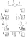
- Fig. 1 shows a schematic of a simplified prior art power window system having, for the purposes of explanation, only a single passenger window.
- the driver's switchplate 10 includes a normally closed lockout switch 12 with which the driver may disable the passenger's auxiliary switch 20.
- the driver's switchplate 10 also has a primary switch 14 to operate the passenger's bi-directional window motor 28.
- the lockout switch 12 When the lockout switch 12 is closed, the auxiliary switch power terminal 22 is supplied with power.
- the auxiliary switch 20 may then be operated by the passenger to raise or lower the window.
- the lockout switch 12 is open, power is not supplied to the auxiliary switch.power terminal 22 and the passenger cannot operate the window.
- the driver's ability to operate the passenger's window is independent of the setting of the lockout switch 14. This is because the driver's primary switch 14 supplies power to the passenger's window through an alternate path, using primary switch power terminal 18 which provides power as long as the ignition is on.
- a driver wishing to operate the passenger's window activates the primary switch 14, which outputs current through primary switch power terminal 18, through one of the normally closed auxiliary switch contacts 24, 26, through the window motor 28, through the other of the normally closed auxiliary switch contacts 24, 26 and then on to ground.
- the power window system described above has a number of drawbacks.
- One of these is that a passenger can interfere with the driver's operation of the passenger's window even when the lockout switch 12 has been activated (opened). This is because electrical continuity must be maintained between the auxiliary switch contacts 24, 26 for the driver to operate the passenger's window. If a passenger were to fiddle with the auxiliary switch 20, he or she would break this continuity and thus interfere with the driver's operation of the passenger's window.
- the present invention is an electrical circuit for a switch with a lockout feature that offers a number of advantages over related prior art devices.
- this invention permits a primary operator (e.g., a driver) to lock out the auxiliary operator (e.g., a passenger) and yet operate the powered device (e.g., window motor) without interference from the auxiliary operator.
- the present invention calls for both the primary operator and the auxiliary operator(s) to activate separate low current mechanical switches to energize the powered device. This feature generally reduces the cost, weight and complexity of the various components used in existing designs.
- high-current switching is performed by power switches responsive to inputs from the low-current lockout and mechanical switches.
- the present invention offers a number of benefits. First, it obviates the need for power wires to be run through the driver's door to a passenger's window motor. Second, it prevents a passenger from interfering with the driver's operation of the passenger's window when the lockout switch has been activated (opened). And third, it reduces the cost and weight of the wiring harnesses needed to implement a power window system, allowing one to run just two control lines from the driver's circuitry to a passenger's door.
- a device made in accordance with the present invention allows both driver and passenger to activate low current mechanical switches which conduct currents less than 20 mA.
- High current switching is performed by mechanical or solid state relays or other equivalent components situated proximate to the motor being actuated. Therefore, the high-current switches are not directly accessible to either the driver or the passenger.
- a general embodiment includes a power source, a bi-directional motor, a lockout switch switchably outputting an ON and an OFF lockout signal, a first primary switch switchably outputting an ON and OFF first primary output signal, a second primary switch switchably outputting an ON and OFF secondary output signal, a first auxiliary switch switchably outputting an ON and an OFF first auxiliary signal, and a second auxiliary switch switchably outputting an ON and an OFF second auxiliary signal.
- first primary circuit which outputs a first tri-state signal responsive to the lockout signal and the first primary signal
- second primary circuit which outputs a second tri-state signal responsive to the lockout signal and the second primary signal
- first auxiliary circuit which outputs a first switching signal responsive to the first auxiliary signal and the first tri-state signal
- second auxiliary circuit which outputs a second switching signal responsive to the second auxiliary signal and the second tri-state signal.
- the circuit includes first and second power switches receiving inputs from the first and second switching signals, the power switches connecting a power supply to two terminals of the bidirectional motor to provide the latter with power.
- the circuit summarized above allows either a primary or an auxiliary user to operate the reversible motor in either a first or a second direction.
- the circuit also provides the primary operator with a lockout switch to prevent the auxiliary operator from operating the motor.
- Outputting dual tri-state signals from the primary circuit requires only two wires, neither of which are power wires, from the primary to the secondary circuits. This contrasts with the three lines necessary in current designs, as shown in Fig. 1, saving the cost and reducing the weight of the required wiring harness.
- Using tri-state signals allows three modes of operation at the auxiliary circuit: lockout OFF which enables the auxiliary operator to operate the motor, lockout ON with the primary operator not activating either primary switch, which disables the auxiliary operator from operating either auxiliary switch, and lockout ON with the primary operator activating one of the two primary switches without enabling the auxiliary operator to activate the auxiliary switch which operates the motor in the opposite direction. Because, in this circuit, all high-current switching is done by components not directly activated by either operator, only low-current switches need be provided to the operators, further saving on costs.
- a circuit in accordance with the present invention provides a primary operator with a low-current mechanical lockout switch L/O and first and second low-current primary switches SW1, SW2. In this embodiment, all three of these switches are normally OFF (open). Closing (i.e., turning ON) one of the two primary switches SW1, SW2 allows the primary operator to operate the bi-directional motor 30 in a first or a second direction, respectively. As explained further below, the first and second primary logic circuitry 60, 80 enables the primary operator to operate the motor regardless of the setting of the lockout switch L/O.
- the first and second primary switches SW1, SW2 preferably are mutually exclusive; i.e., only one of them can be activated at a time. This can be ensured, for instance, by using a double throw contact (i.e., non-latching) switch, preferably a rocker type.
- the lockout switch L/O in contrast, is preferably a latching single throw switch.
- the circuit also provides an auxiliary operator with normally OFF, low-current first and second auxiliary switches SW3, SW4, respectively. So long as the lockout switch L/O is not activated, an auxiliary operator can operate the bidirectional motor 30 in a first or a second direction by activating one of low-current first and second auxiliary switches SW3 and SW4, respectively.
- first and second auxiliary switches SW3, SW4 preferably are mutually exclusive and also may be combined into a second double throw contact rocker switch.
- First and second primary logic circuits 60, 80 both receive an input from the lockout switch L/O. Each also receives a second input from corresponding first and second primary switches SW1, SW2, respectively. First and second primary logic circuits 60, 80 supply a tri-state output in response to the setting of the lockout switch L/O and activations of first and second primary switches SW1, SW2.
- the three states are labeled HI, LO and X.
- a primary logic circuit's output is HI whenever the corresponding primary switch is activated (ON) regardless of the status of the lockout switch L/O; its output is LO when the lockout switch L/O is activated (ON) and the corresponding primary switch is not activated (OFF); and its output is X if both the lockout switch L/O and the corresponding primary switch are not activated (OFF). Because first and second primary switches SW1, SW2 are preferably mutually exclusive, outputs from first and second primary logic circuits 60, 80 cannot simultaneously be HI. They may, however, both be LO or X.
- the first and second auxiliary logic circuits 70, 90 each receive two inputs. One input to each is the aforementioned tri-state output from corresponding first and second primary logic circuit 60, 80, respectively.
- the second input to first and second auxiliary logic circuits 70, 90 is from normally OFF first and second auxiliary switch SW3, SW4, respectively.
- the first and second auxiliary logic circuits 70, 90 each supply a signal having a two-level output (ON or OFF), the output level being determined by the inputs received by each.
- An auxiliary logic circuit's output level is ON in two instances: 1) whenever its tri-state input is HI and 2) when its tri-state input is X and the corresponding auxiliary switch is ON.
- An auxiliary logic circuit's output is OFF at all other times.
- the first and second auxiliary logic circuits 70, 90 supply their respective outputs to the first and second power switches 50, 52, respectively.
- First and second power switches 50, 52 are high-current switches that are activated by an ON output level from first and second auxiliary logic circuits 70, 90, respectively. When either power switch is activated, it completes an electrical circuit by connecting a power source to one of two normally grounded terminals 32, 34 of the bi-directional motor 30.
- the first and second power switches 50, 52 preferably are mutually exclusive so that when one is closed, the other must remain open. This prevents both terminals of the motor from simultaneously being connected to the power source which would turn off the motor.
- the first and second power switches 50, 52 may be made mutually exclusive by implementing one dual relay which selectively connects an input (e.g., a power source) to energize only one of two outputs (e.g., the terminals on the motor). This could also be done with H-bridge drivers implemented with FETs or BJTs, as known to those skilled in the art.
- the primary and auxiliary logic circuits whose functions are described above can be implemented by using different types of components providing the same logic functions. As known by those skilled in the art, discrete analog components, integrated circuits, digital logic gates, microprocessors, programmable logic arrays and analog comparators may all be employed for this purpose.
- first and second primary circuits could be combined into a single three-input, two-output circuit wherein the two outputs are tri-state outputs.
- first and second auxiliary circuits could be combined into a single four-input, two-output circuit. It makes no difference how one characterizes either the primary circuits or the auxiliary circuits; it is the input-output relationship of these circuits that counts. It should also be noted that combining either or both pairs of circuits may be done with any of the types of components listed above.
- the invention may be used in any number of settings where a primary and an auxiliary operator both need to operate a high current motor by activating only low-current switches with the primary operator being provided with the additional capability of locking out the auxiliary operator by activating a low-current lockout switch.
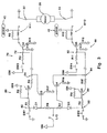
- Fig. 3 presents an analog implementation of the logic circuitry of the invention that is suitable for controlling a window on a passenger vehicle.
- Non-latching contact switches SW1 and SW2 enable the driver to operate a passenger's window (not shown) while non-latching contact switches SW3 and SW4 enable a passenger that window.
- the functions served by driver switches SW1 and SW2 preferably are combined into a single double throw contact rocker switch.
- passenger switches SW3 and SW4 As known to those skilled in the art, such rocker switches are normally in a neutral position and may be selectively activated to either raise or lower a window motor.
- the lockout switch L/O preferably a single throw latching switch, is accessible only to the driver and serves to prevent the passenger from operating his window. With the lockout switch L/O not activated (open), either driver switch SW1 or passenger switch SW3 can be activated to operate the window in a first direction. Similarly, either driver switch SW2 or passenger switch SW4 can be activated to operate the window in a second, opposite direction. Without loss of generality, we will assume that activating either SW1 or SW3 causes the window to go UP (thus raising the window) and activating either SW2 or SW4 causes the window to go DOWN (thus lowering the window).
- the circuit of Fig. 3 comprises the aforementioned manually operated switches, driver UP circuit, shown generally as 60, passenger UP circuit, shown generally as 70, driver DOWN circuit, shown generally as 80, passenger DOWN circuit, shown generally as 90, UP relay RY1, DOWN relay RY2 and the bi-directional motor 30 with normally grounded terminals 32, 34.
- Power to the overall circuit is provided via an ignition-switched power relay (not shown) whose voltage is represented by 'IGN' in Fig. 3.
- the driver UP input node 62 and the base and emitter electrodes of the driver UP transistor Q1 are all held at a voltage of IGN. Because Q1's base-emitter junction is not reversed biased, Q1 is off and current does not flow through either Q1 current limiting resistor R1 or Q1 shunt resistor R2. Consequently, Q1's collector does not conduct and no current flows through Q1's collector resistor R3 interposed between Q1's collector and the driver UP output node 64. Because neither Q1 nor Q3 are conducting, the driver UP output node 64 is neither pulled to ground (LO), nor raised to IGN voltage (HI). Instead, it is effectively open circuited, causing the driver UP circuit 60 to output a signal having a floating level of X.
- R1 is 10k ⁇
- R2 is 100k ⁇
- Q1 is an MPSA56.
- a collector current flows through Q1's collector resistor R3, which is preferably 680 ⁇ , and an emitter-collector voltage, typically 200-300 mV below IGN appears at Q1's collector.
- the voltage at the driver UP output node 64 is about 1.6-1.8 V, causing the driver UP circuit 60 to output a signal having a level that is HI.
- the driver UP circuit 60 When L/O is activated (closed or ON), the driver UP circuit 60 operates somewhat differently. Closing L/O causes the potential at the anode of UP bypass diode D1 to assume a voltage close to 0.8 V. This allows the base-emitter junction of Q3 to become forward biased, turning on Q3 and causing a current to flow through the current limiting UP lockout resistor R6. When it is turned on, Q3 has a very low collector-emitter voltage, pulling the driver UP output node 64 close to ground and providing a path for current to flow from the driver UP output node 64 to ground via Q3's emitter resistor R17.
- Q3 turns off because the voltage drop across D1 (and thus Q3's base voltage) is on the order of 0.65 V, such a low base-emitter voltage being insufficient to keep Q3 on.
- UP bypass diode D1 causes Q3 to turn off when SW1 is activated.
- driver UP transistor Q1 whose base-emitter junction is now reverse biased, begins conducting. This causes the driver UP output node 64 to assume a voltage about 1.6-1.8 V, resulting in driver UP circuit 60 to output a signal having a level that is HI.
- the driver UP circuit outputs a HI signal whenever driver UP switch SW1 is activated (ON) regardless of the L/O setting, outputs a LO signal when the L/O switch is activated (ON) and SW1 is not activated (OFF), and outputs a signal of level X when both the L/O and the SW1 switches are not activated (OFF).
- the output of the driver UP circuit 60 is electrically connected to the passenger UP circuit 70 at the passenger UP input node 72.
- UP input node 72 is connected to the base electrode of passenger UP transistor Q2.
- Q2's base is connected to ground by Q2's pull-down resistor R13 to ensure that leakage current does not turn on Q2.
- Q2's emitter is connected to ground by R15, which forces node 72 up to about 1.1V, thus ensuring that even with a ground offset of 0.5V, Q3 will be able to turn Q2 off.
- the passenger UP input node 72 also receives an input from the passenger UP switch SW3 via Q2's current limiting resistor R4.
- R4 is 2.2K ⁇
- R13 is 33K ⁇
- R15 is 10 ⁇
- Q2 is an MPSA06. It should be noted, however, that R15's value depends on the type of switch used (e.g., relay, FET, BJT, etc.) and the resistance associated with it.
- the driver UP circuit 60 When the driver UP circuit 60 outputs a HI signal, (i.e., the driver UP switch SW1 is ON), Q2 base-emitter junction is forward biased, turning on Q2 and causing current to flow through Q2's collector.
- Q2 is turned on when either the driver activates SW1 or the passenger activates SW3 with the L/O switch open. Turning on Q2 causes a current to flow through Q2's collector and activates the power switch by either energizing a relay coil or turning on a solid state power switch (i.e., FET or BJT).
- Q2's load resistor R5 is shunted across a pair of input terminals to UP relay RY1, reducing inductive spikes from the relay coil.
- R5 is 820 ⁇ and RY1 is 225 ⁇ .
- RY1 serves as a high-current power switch, closing a connection from IGN to a first terminal 32 of the bi-directional motor 30, causing the motor to raise the corresponding passenger window (not shown) when Q2 is turned on.
- the window is operated by energizing bidirectional motor 30 whose first and second terminals 32, 34 are normally grounded.
- Energizing UP relay RY1 by turning on Q2 allows current to flow in one direction from IGN through the first motor terminal 32, through the bi-directional motor 30 and therefrom to ground via the second motor terminal 34.
- UP relay RY1 and its counterpart DOWN relay RY2 are mutually exclusive so that as long as RY1 is closed, RY2 remains open. This prevents both first and second motor terminals 32, 34 from being connected to the power source at the same time.
- This function can be achieved by employing a dual relay such as part number EP2-3N1S, familiar to those skilled in the art of analog circuit design. Two single relays with appropriate lockout circuitry may also be used, for this purpose.
- Driver DOWN circuit shown generally as 80, uses driver DOWN switch SW2, DOWN lockout resistor R7, DOWN bypass diode D2, DOWN lockout transistor Q4, Q4 emitter resistor R18, driver DOWN input node 82, driver DOWN transistor Q5, driver DOWN output node 84, Q5's current limiting resistor R8, Q5's shunt resistor R9 and Q5's collector resistor R10 in place of the corresponding driver UP circuit components.
- Passenger DOWN circuit shown generally as 90, is similarly comprised of passenger DOWN switch SW4, passenger DOWN transistor Q6, passenger DOWN input node 92 connected to Q6's base, Q6's pull-down resistor R14, Q6's current limiting resistor R11, Q6 emitter resistor R16, Q6's base load resistor R12, and DOWN relay RY2.
- Closing RY2 by activating either SW2 or SW4 with the L/O switch not activated connects IGN to the second terminal 34 of the bi-directional motor 30.
- the components in the DOWN circuitry are identical to those in the UP circuitry whose operation is detailed above.
- driver UP and driver DOWN circuits and the passenger UP and passenger DOWN circuits have been cast as discrete subsystems of the invention, this characterization is not critical.
- the driver UP and driver DOWN circuits are symmetric as are the passenger UP and passenger DOWN circuits. Therefore, without changing either the spirit or scope of the present invention, the driver UP and driver DOWN circuits can be recast as a single three-input (lockout and the two driver switches), two-output circuit.
- the passenger UP and the passenger DOWN circuits can be recast as a single four input (two outputs from the driver circuit and the two passenger switches), two output circuit. Recasting the above implementation in this manner preserves the objectives of the present invention.
- a switch system having a plurality of the circuits of Fig. 3 and provide the driver with a common lockout switch.
- Such a system is suitable in settings where a number of windows, each operable by a separate set of primary and auxiliary switches, must be controlled.
- a familiar example of this is a passenger vehicle having a driver window and three passenger windows, the latter provided with switches operable by either the driver or the various passengers with the driver further provided with a lockout switch.
- Providing a single, common lockout switch permits the driver to disable all the auxiliary switches at once while retaining the ability to operate any one or more of them in the manner discussed above. Needless to say, there is no theoretical limit to the number passenger windows that can be controlled; one need only incorporate one such circuit per passenger window to be controlled.
- circuit diagram presented in Fig. 3 is intended for controlling a passenger window, there is no reason why such a circuit cannot be employed in other settings as well.
- the invention may be employed in any setting calling for a primary operator and a plurality of auxiliary operators to use low-current switches to indirectly activate a high-current switch to operate a bi-directional motor wherein the primary operator is also provided with a low-current lockout switch.
- One such application is the control of power door locks in a passenger vehicle wherein a solenoid or other actuator movable between a locked and an unlocked state is controlled in a similar manner by the circuitry described above. Again, all high-current power switching is performed at the actuator by a relay or the like while the driver and the passenger operate only low current switches.
Landscapes
- Engineering & Computer Science (AREA)
- Power Engineering (AREA)
- Window Of Vehicle (AREA)
- Power-Operated Mechanisms For Wings (AREA)
- Motor And Converter Starters (AREA)
- Stopping Of Electric Motors (AREA)
- Control Of Motors That Do Not Use Commutators (AREA)
- Input Circuits Of Receivers And Coupling Of Receivers And Audio Equipment (AREA)
- Dc-Dc Converters (AREA)
- Lock And Its Accessories (AREA)
- Control Of Multiple Motors (AREA)
Abstract
Description
Claims (20)
- An electrical circuit for selectively activating a bi-directional motor (30) in a first or second direction comprising:wherein said bi-directional motor (30) is operated in said first direction by switching ON one of said first primary switch (SW1) and said first auxiliary switch (SW3) and said bi-directional motor (30) is operated in said second direction by switching ON one of said second primary switch (SW2) and said second auxiliary switch, said first and second auxiliary switches causing said motor (30) to operate only when said lockout switch (L/O) is OFF.a power source (40);a bi-directional motor (30) having a first and a second motor terminal (32 and 34 respectively);a lockout switch (L/O) switchable between an ON and an OFF position, said lockout switch (L/O) outputting a lockout signal reflective of said lockout switch (L/O) position;a first primary switch (SW1) switchable between an ON and an OFF position, said first primary switch (SW1) outputting a first primary signal reflective of said first primary switch (SW1) position;a second primary switch (SW2) switchable between an ON and an OFF position, said second primary switch (SW2) outputting a second primary signal reflective of said second primary switch (SW2) position;a first auxiliary switch (SW3) switchable between an ON and an OFF position, said first auxiliary switch (SW3) outputting a first auxiliary signal reflective of said first auxiliary switch (SW3) position;a second auxiliary switch (SW4) switchable between an ON and an OFF position, said second auxiliary switch outputting a second auxiliary signal reflective of said second auxiliary switch position;a primary circuit (60,80) having means for supplying a first tri-state signal having a level responsive to said lockout signal and said first primary signal, and a second tri-state signal having a level responsive to said lockout signal and said second primary signal;an auxiliary circuit (70, 90) having means for supplying a first switching signal having a level responsive to said first auxiliary signal and said first tri-state signal, and a second switching signal having a level responsive to said second auxiliary signal and said second tri-state signal;a first power switch (50) for connecting said power source to said first (32) terminal in response to said first switching signal;a second power switch (52) for connecting said power source to said second motor terminal (34) in response to said second switching signal;
- The electrical circuit of claim 1, wherein said first tri-state signal is HI when said first primary signal is ON, said first tri-state signal is LO when said first primary signal is OFF and said lockout signal is ON, and said first tri-state signal is 'X' when said first primary signal is OFF and said lockout signal is OFF, and said second tri-state signal is HI when said second primary signal is ON, said second tri-state signal is LO when said second primary signal is OFF and said lockout signal is ON, and said second tri-state signal is 'X' when said second primary signal is OFF and said lockout signal is OFF.
- The electrical circuit of claim 1, wherein said first switching signal is ON when said first tri-state signal is HI, said first switching signal is OFF when said first tri-state signal is LO, and said first switching signal is ON when said first tri-state signal is 'X' and said first auxiliary signal is ON, and said second switching signal is ON when said second tri-state signal is HI, said second switching signal is OFF when said second tri-state signal is LO, and said second switching signal is ON when said second tri-state signal is 'X' and said second auxiliary signal is ON.
- The electrical circuit of any of the preceding claims, wherein said first and second power switches (50 and 52 respectively) are mutually exclusive.
- The electrical circuit of claim 4, wherein said first and second power switches (50 and 52) are combined into a dual relay.
- The electrical circuit of claim 1 wherein said first and second primary switches (SW1 and SW2 respectively) are mutually exclusive and said first and second auxiliary switches (SW3 and SW4 respectively) are mutually exclusive.
- The electrical circuit of any of the preceding claims, wherein said first and second primary switches (SW1 and SW2 respectively) are combined into a primary double throw contact rocker switch and said first and second auxiliary switches (SW3 and SW4 respectively) are combined into an auxiliary double throw contact rocker switch.
- The electrical circuit of any of the preceding claims, wherein said primary circuit (60,80) further comprises a first primary circuit (60) having means for supplying said first tri-state signal having a level responsive to said lockout signal and said first primary signal, and a second primary circuit (60,80) having means for supplying said second tri-state signal having a level responsive to said lockout signal and said second primary signal.
- The electrical circuit of any of the preceding claims, wherein said auxiliary circuit (70,90) further comprises a first auxiliary circuit (70) having means for supplying said first switchmgi signal having a level responsive to said first tri-state signal and said first auxiliary signal, and a second auxiliary circuit (90) having means for supplying said second switching signal having a level responsive to said second tri-state signal and said second auxiliary signal.
- An electrical circuit as claimed in claim 1, wherein the bi-directional motor (30) is a window motor (30); the lockout switch (L/O) is a driver lockout switch; the first and second primary switches (SW1 and SW2 respectively) are combined into a normally neutral driver switch selectively switchable from said neutral position to one of an UP position and a DOWN position, said driver switch outputting a driver UP signal reflecting said driver switch being in said UP position and said driver switch outputting a driver DOWN signal reflecting said driver switch being in said DOWN position; the first and second auxiliary switches comprise a normally neutral passenger switch selectively switchable from said neutral position to one of an UP position and a DOWN position, said passenger switch outputting a passenger UP signal reflecting said passenger switch being in said UP position and said passenger switch outputting a passenger DOWN signal reflecting said passenger switch being in said DOWN position; the primary circuit (60) comprises a driver UP circuit having means for supplying an UP tri-state signal, said UP tri-state signal having a level responsive to said lockout signal and said driver UP signal, and a driver DOWN circuit having means for supplying a DOWN tri-state signal, said DOWN tri-state signal having a level responsive to said lockout signal and said driver DOWN signal; the auxiliary circuit has a passenger UP circuit having means for supplying an UP switching signal having a level responsive to said UP tri-state signal and said passenger UP signal, and a passenger DOWN circuit having means for supplying a DOWN switching signal having a level responsive to said DOWN tri-state signal and said passenger DOWN signal; the first power switch (50) is an UP power switch for connecting said power source to said first window motor terminal (32) in response to said UP switching signal, and the second power switch (52) is a DOWN power switch for connecting said power source to said second window motor (34) terminal in response to said DOWN switching signal.
- The, electrical circuit of claim 10, wherein said driver UP circuit means comprises a driver UP input node receiving an input from said driver UP signal, a driver UP output node, a driver UP transistor interposed between said drive UP input node and said driver UP output node, said driver UP transistor supplying a driver UP transistor signal responsive to said driver UP signal.
- The electrical circuit of claim 11, wherein said driver UP circuit means further comprises a shunt resistor interposed between a base electrode and an emitter electrode of said driver UP transistor.
- The electrical circuit of claim 11 wherein said driver UP circuit means further comprises an UP lockout transistor supplying an UP lockout transistor signal to said driver UP output node, said UP lockout transistor signal having a level responsive to said lockout signal and an UP bypass diode for disabling said UP lockout transistor, said UP bypass diode responsive to said driver UP signal.
- The electrical circuit of claim 10, wherein said driver DOWN circuit means comprises a driver DOWN input node, a driver DOWN output node, a driver DOWN transistor interposed between said driver DOWN input node and said driver DOWN output node, said driver DOWN transistor supplying a driver DOWN transistor signal responsive to said driver DOWN signal.
- The electrical circuit of claim 14, wherein said driver DOWN circuit means further comprises a shunt resistor interposed between a base electrode and an emitter electrode of said driver DOWN transistor.
- The electrical circuit of claim 14, wherein said driver DOWN circuit means further comprises a DOWN lockout transistor supplying a DOWN lockout transistor signal to said driver DOWN output node, said DOWN lockout transistor signal having a level responsive to said lockout signal, and a DOWN bypass diode for disabling said DOWN lockout transistor, said DOWN bypass diode responsive to said driver DOWN signal.
- The electrical circuit of claim 10, wherein said passenger UP circuit means comprises a passenger UP input node receiving a first input from said passenger UP signal and a second input from said UP tri-state signal, an output node supplying said UP switching signal, and a passenger UP transistor interposed between said passenger UP input node and said passenger UP output node.
- The electrical circuit of claim 10, wherein said passenger DOWN circuit means comprises a passenger DOWN input node receiving a first input from said passenger DOWN signal and a second input from said DOWN tri-state signal, an output node supplying said DOWN switching signal, and a passenger DOWN transistor interposed between said passenger DOWN input node and said passenger DOWN output node.
- An electrical circuit as claimed in claim 1 for controlling a passenger window in a passenger vehicle, wherein the motor (30) is a window motor (30); the lockout is a driver lockout switch; the first and second primary switches (SW1 and SW2 respectively) are combined into a normally neutral driver switch selectively switchable from said neutral position to one of an UP position and a DOWN position, said driver switch outputting a driver UP signal reflecting said driver switch being in said UP position and said driver switch outputting a driver DOWN signal reflecting said driver switch being in said DOWN position; the first and second auxiliary switches are combined into a normally neutral passenger switch selectively switchable from said neutral position to one of an UP position and a DOWN position, said passenger switch outputting a passenger UP signal reflecting said passenger switch being in said UP position and said passenger switch outputting a passenger DOWN signal reflecting said passenger switch being in said DOWN position; the primary circuit (60,80) is a driver circuit having means for supplying an UP tri-state signal, said UP tri-state signal having a level responsive to said lockout signal and said driver UP signal, and a DOWN tri-state signal, said DOWN tri-state signal having a level responsive to said lockout signal and said driver DOWN signal; the auxiliary circuit (70,90) is a passenger circuit having means for supplying an UP switching signal having a level responsive to said UP tri-state signal and said passenger UP signal, and a DOWN switching signal having a level responsive to said DOWN tri-state signal and said passenger DOWN signal; the first power switch (50) is an UP power switch for connecting said power source to said first window motor terminal (32) in response to said UP switching signal; and the second power switch (52) is a DOWN power switch for connecting said power source to said second window motor terminal (34) in response to said DOWN switching signal.
- The electrical circuit of claim 10, wherein said first and second motor terminals (32 and 34 respectively) are normally grounded.
Applications Claiming Priority (3)
| Application Number | Priority Date | Filing Date | Title |
|---|---|---|---|
| US530496 | 1995-09-19 | ||
| US08/530,496 US5627411A (en) | 1995-09-19 | 1995-09-19 | Switching circuit with lockout feature |
| PCT/US1996/014887 WO1997011523A1 (en) | 1995-09-19 | 1996-09-17 | Switching circuit with lockout feature |
Publications (3)
| Publication Number | Publication Date |
|---|---|
| EP0852084A1 EP0852084A1 (en) | 1998-07-08 |
| EP0852084A4 EP0852084A4 (en) | 1999-01-07 |
| EP0852084B1 true EP0852084B1 (en) | 2005-11-23 |
Family
ID=24113830
Family Applications (1)
| Application Number | Title | Priority Date | Filing Date |
|---|---|---|---|
| EP96933805A Expired - Lifetime EP0852084B1 (en) | 1995-09-19 | 1996-09-17 | Switching circuit with lockout feature |
Country Status (10)
| Country | Link |
|---|---|
| US (1) | US5627411A (en) |
| EP (1) | EP0852084B1 (en) |
| JP (1) | JP3255927B2 (en) |
| CN (1) | CN1201565A (en) |
| AT (1) | ATE311035T1 (en) |
| AU (1) | AU7239796A (en) |
| BR (1) | BR9610639A (en) |
| DE (1) | DE69635483T2 (en) |
| MX (1) | MX9802248A (en) |
| WO (1) | WO1997011523A1 (en) |
Families Citing this family (8)
| Publication number | Priority date | Publication date | Assignee | Title |
|---|---|---|---|---|
| JP3759293B2 (en) * | 1997-08-08 | 2006-03-22 | 本田技研工業株式会社 | Power window drive circuit |
| JP3479737B2 (en) * | 1998-04-09 | 2003-12-15 | 東洋電装株式会社 | Power window device |
| US6671144B1 (en) | 2000-06-26 | 2003-12-30 | Premier Aviation, Inc. | Method and apparatus for detecting ground faults and for isolating power supply from the ground faults |
| EP1303897A1 (en) * | 2000-06-26 | 2003-04-23 | Premier Aviation, Inc. | Method and apparatus for detecting electrical faults and isolating power source from the electrical faults |
| JP2005273421A (en) * | 2004-03-26 | 2005-10-06 | Honda Motor Co Ltd | Power window system |
| JP4254703B2 (en) * | 2004-12-07 | 2009-04-15 | 株式会社デンソー | Inductive load drive |
| CN101997468B (en) * | 2009-08-17 | 2014-08-20 | 樱花卫厨(中国)股份有限公司 | Motor constant-speed forward/reverse rotation control circuit |
| CN110919081B (en) * | 2018-09-18 | 2022-11-11 | 南京泉峰科技有限公司 | Electric tool |
Family Cites Families (3)
| Publication number | Priority date | Publication date | Assignee | Title |
|---|---|---|---|---|
| US3688173A (en) * | 1971-08-27 | 1972-08-29 | Physical Electronics Ind Inc | Solid state window controls |
| US4146826A (en) * | 1976-01-26 | 1979-03-27 | Rca Corporation | Gto bi-directional motor control circuit |
| US5149924A (en) * | 1989-05-05 | 1992-09-22 | Priesemuth W | Multiple contact switch arrangement |
-
1995
- 1995-09-19 US US08/530,496 patent/US5627411A/en not_active Expired - Lifetime
-
1996
- 1996-09-17 WO PCT/US1996/014887 patent/WO1997011523A1/en not_active Ceased
- 1996-09-17 AT AT96933805T patent/ATE311035T1/en not_active IP Right Cessation
- 1996-09-17 JP JP51283597A patent/JP3255927B2/en not_active Expired - Lifetime
- 1996-09-17 DE DE69635483T patent/DE69635483T2/en not_active Expired - Fee Related
- 1996-09-17 EP EP96933805A patent/EP0852084B1/en not_active Expired - Lifetime
- 1996-09-17 CN CN96198165A patent/CN1201565A/en active Pending
- 1996-09-17 BR BR9610639-5A patent/BR9610639A/en not_active IP Right Cessation
- 1996-09-17 AU AU72397/96A patent/AU7239796A/en not_active Abandoned
-
1998
- 1998-03-20 MX MX9802248A patent/MX9802248A/en unknown
Also Published As
| Publication number | Publication date |
|---|---|
| DE69635483T2 (en) | 2006-08-24 |
| US5627411A (en) | 1997-05-06 |
| MX9802248A (en) | 1998-11-30 |
| AU7239796A (en) | 1997-04-09 |
| JPH11511640A (en) | 1999-10-05 |
| EP0852084A4 (en) | 1999-01-07 |
| WO1997011523A1 (en) | 1997-03-27 |
| EP0852084A1 (en) | 1998-07-08 |
| JP3255927B2 (en) | 2002-02-12 |
| DE69635483D1 (en) | 2005-12-29 |
| ATE311035T1 (en) | 2005-12-15 |
| CN1201565A (en) | 1998-12-09 |
| BR9610639A (en) | 1999-12-21 |
Similar Documents
| Publication | Publication Date | Title |
|---|---|---|
| CA1222305A (en) | Vehicle power window control circuit | |
| US5549984A (en) | Control and indicator circuit for a dual battery system | |
| US8710773B2 (en) | Vehicle window opening and closing control device | |
| JPH0650825B2 (en) | Wireless telephone | |
| EP0852084B1 (en) | Switching circuit with lockout feature | |
| US4649286A (en) | Power supply circuit for vehicle | |
| US5572098A (en) | Motor vehicle accessory control with control module having single power terminal | |
| US5331260A (en) | System for controlling power windows of vehicles | |
| US5192873A (en) | Fail-operational control system for vehicle loads | |
| CA2232690C (en) | Switching circuit with lockout feature | |
| CA1222042A (en) | Control circuit for locking mechanism of sliding vehicle door | |
| US6111326A (en) | Control circuit for opening/closing device in a vehicle | |
| US3745362A (en) | Two relay control circuit for automotive vehicles | |
| US4897632A (en) | Power door lock interlock circuit | |
| JPH048587B2 (en) | ||
| US4789851A (en) | Power door lock interlock circuit | |
| US6150854A (en) | Circuit arrangement for switching an inductive load | |
| US20190326905A1 (en) | Load driving device | |
| US6417636B2 (en) | Power window device | |
| US7282817B2 (en) | Electrical circuit arrangement for controlling an electromotor in a motor vehicle | |
| US4543514A (en) | Central locking system for motor vehicles | |
| US20090153226A1 (en) | High-side driver for providing an off-state in case of ground loss | |
| KR200286230Y1 (en) | Motor driving apparatus, used in an apparatus for automatically opening/closing the door of an automobile, in which a circuit in two stages of tr is comprised | |
| JP2000268660A (en) | Power window switch circuit | |
| US20030107861A1 (en) | Method and apparatus for disconnecting a battery |
Legal Events
| Date | Code | Title | Description |
|---|---|---|---|
| PUAI | Public reference made under article 153(3) epc to a published international application that has entered the european phase |
Free format text: ORIGINAL CODE: 0009012 |
|
| 17P | Request for examination filed |
Effective date: 19980402 |
|
| AK | Designated contracting states |
Kind code of ref document: A1 Designated state(s): AT BE CH DE DK ES FI FR GB GR IE IT LI LU MC NL PT SE |
|
| RIN1 | Information on inventor provided before grant (corrected) |
Inventor name: BOCHENEK, JEFFREY |
|
| A4 | Supplementary search report drawn up and despatched |
Effective date: 19981119 |
|
| AK | Designated contracting states |
Kind code of ref document: A4 Designated state(s): AT BE CH DE DK ES FI FR GB GR IE IT LI LU MC NL PT SE |
|
| 17Q | First examination report despatched |
Effective date: 20040108 |
|
| GRAP | Despatch of communication of intention to grant a patent |
Free format text: ORIGINAL CODE: EPIDOSNIGR1 |
|
| GRAS | Grant fee paid |
Free format text: ORIGINAL CODE: EPIDOSNIGR3 |
|
| GRAA | (expected) grant |
Free format text: ORIGINAL CODE: 0009210 |
|
| RAP1 | Party data changed (applicant data changed or rights of an application transferred) |
Owner name: C-MAC INVOTRONICS INC. |
|
| AK | Designated contracting states |
Kind code of ref document: B1 Designated state(s): AT BE CH DE DK ES FI FR GB GR IE IT LI LU MC NL PT SE |
|
| PG25 | Lapsed in a contracting state [announced via postgrant information from national office to epo] |
Ref country code: NL Free format text: LAPSE BECAUSE OF FAILURE TO SUBMIT A TRANSLATION OF THE DESCRIPTION OR TO PAY THE FEE WITHIN THE PRESCRIBED TIME-LIMIT Effective date: 20051123 Ref country code: LI Free format text: LAPSE BECAUSE OF FAILURE TO SUBMIT A TRANSLATION OF THE DESCRIPTION OR TO PAY THE FEE WITHIN THE PRESCRIBED TIME-LIMIT Effective date: 20051123 Ref country code: FI Free format text: LAPSE BECAUSE OF FAILURE TO SUBMIT A TRANSLATION OF THE DESCRIPTION OR TO PAY THE FEE WITHIN THE PRESCRIBED TIME-LIMIT Effective date: 20051123 Ref country code: CH Free format text: LAPSE BECAUSE OF FAILURE TO SUBMIT A TRANSLATION OF THE DESCRIPTION OR TO PAY THE FEE WITHIN THE PRESCRIBED TIME-LIMIT Effective date: 20051123 Ref country code: BE Free format text: LAPSE BECAUSE OF FAILURE TO SUBMIT A TRANSLATION OF THE DESCRIPTION OR TO PAY THE FEE WITHIN THE PRESCRIBED TIME-LIMIT Effective date: 20051123 Ref country code: AT Free format text: LAPSE BECAUSE OF FAILURE TO SUBMIT A TRANSLATION OF THE DESCRIPTION OR TO PAY THE FEE WITHIN THE PRESCRIBED TIME-LIMIT Effective date: 20051123 |
|
| REG | Reference to a national code |
Ref country code: GB Ref legal event code: FG4D |
|
| REG | Reference to a national code |
Ref country code: CH Ref legal event code: EP |
|
| REF | Corresponds to: |
Ref document number: 69635483 Country of ref document: DE Date of ref document: 20051229 Kind code of ref document: P |
|
| REG | Reference to a national code |
Ref country code: IE Ref legal event code: FG4D |
|
| PG25 | Lapsed in a contracting state [announced via postgrant information from national office to epo] |
Ref country code: SE Free format text: LAPSE BECAUSE OF FAILURE TO SUBMIT A TRANSLATION OF THE DESCRIPTION OR TO PAY THE FEE WITHIN THE PRESCRIBED TIME-LIMIT Effective date: 20060223 Ref country code: GR Free format text: LAPSE BECAUSE OF FAILURE TO SUBMIT A TRANSLATION OF THE DESCRIPTION OR TO PAY THE FEE WITHIN THE PRESCRIBED TIME-LIMIT Effective date: 20060223 Ref country code: DK Free format text: LAPSE BECAUSE OF FAILURE TO SUBMIT A TRANSLATION OF THE DESCRIPTION OR TO PAY THE FEE WITHIN THE PRESCRIBED TIME-LIMIT Effective date: 20060223 |
|
| PG25 | Lapsed in a contracting state [announced via postgrant information from national office to epo] |
Ref country code: ES Free format text: LAPSE BECAUSE OF FAILURE TO SUBMIT A TRANSLATION OF THE DESCRIPTION OR TO PAY THE FEE WITHIN THE PRESCRIBED TIME-LIMIT Effective date: 20060306 |
|
| PG25 | Lapsed in a contracting state [announced via postgrant information from national office to epo] |
Ref country code: PT Free format text: LAPSE BECAUSE OF FAILURE TO SUBMIT A TRANSLATION OF THE DESCRIPTION OR TO PAY THE FEE WITHIN THE PRESCRIBED TIME-LIMIT Effective date: 20060424 |
|
| NLV1 | Nl: lapsed or annulled due to failure to fulfill the requirements of art. 29p and 29m of the patents act | ||
| REG | Reference to a national code |
Ref country code: CH Ref legal event code: PL |
|
| ET | Fr: translation filed | ||
| PG25 | Lapsed in a contracting state [announced via postgrant information from national office to epo] |
Ref country code: IE Free format text: LAPSE BECAUSE OF NON-PAYMENT OF DUE FEES Effective date: 20060918 |
|
| PLBE | No opposition filed within time limit |
Free format text: ORIGINAL CODE: 0009261 |
|
| STAA | Information on the status of an ep patent application or granted ep patent |
Free format text: STATUS: NO OPPOSITION FILED WITHIN TIME LIMIT |
|
| PG25 | Lapsed in a contracting state [announced via postgrant information from national office to epo] |
Ref country code: MC Free format text: LAPSE BECAUSE OF NON-PAYMENT OF DUE FEES Effective date: 20060930 |
|
| 26N | No opposition filed |
Effective date: 20060824 |
|
| REG | Reference to a national code |
Ref country code: IE Ref legal event code: MM4A |
|
| PG25 | Lapsed in a contracting state [announced via postgrant information from national office to epo] |
Ref country code: LU Free format text: LAPSE BECAUSE OF NON-PAYMENT OF DUE FEES Effective date: 20060917 |
|
| PGFP | Annual fee paid to national office [announced via postgrant information from national office to epo] |
Ref country code: IT Payment date: 20080926 Year of fee payment: 13 Ref country code: FR Payment date: 20080917 Year of fee payment: 13 |
|
| PGFP | Annual fee paid to national office [announced via postgrant information from national office to epo] |
Ref country code: GB Payment date: 20080929 Year of fee payment: 13 |
|
| PGFP | Annual fee paid to national office [announced via postgrant information from national office to epo] |
Ref country code: DE Payment date: 20081031 Year of fee payment: 13 |
|
| GBPC | Gb: european patent ceased through non-payment of renewal fee |
Effective date: 20090917 |
|
| REG | Reference to a national code |
Ref country code: FR Ref legal event code: ST Effective date: 20100531 |
|
| PG25 | Lapsed in a contracting state [announced via postgrant information from national office to epo] |
Ref country code: FR Free format text: LAPSE BECAUSE OF NON-PAYMENT OF DUE FEES Effective date: 20090930 Ref country code: DE Free format text: LAPSE BECAUSE OF NON-PAYMENT OF DUE FEES Effective date: 20100401 |
|
| PG25 | Lapsed in a contracting state [announced via postgrant information from national office to epo] |
Ref country code: GB Free format text: LAPSE BECAUSE OF NON-PAYMENT OF DUE FEES Effective date: 20090917 |
|
| PG25 | Lapsed in a contracting state [announced via postgrant information from national office to epo] |
Ref country code: IT Free format text: LAPSE BECAUSE OF NON-PAYMENT OF DUE FEES Effective date: 20090917 |