EP0851252A1 - Temperature independent optical multiplexer and/or demultiplexer - Google Patents
Temperature independent optical multiplexer and/or demultiplexer Download PDFInfo
- Publication number
- EP0851252A1 EP0851252A1 EP97403114A EP97403114A EP0851252A1 EP 0851252 A1 EP0851252 A1 EP 0851252A1 EP 97403114 A EP97403114 A EP 97403114A EP 97403114 A EP97403114 A EP 97403114A EP 0851252 A1 EP0851252 A1 EP 0851252A1
- Authority
- EP
- European Patent Office
- Prior art keywords
- sections
- guide
- section
- temperature
- fact
- Prior art date
- Legal status (The legal status is an assumption and is not a legal conclusion. Google has not performed a legal analysis and makes no representation as to the accuracy of the status listed.)
- Withdrawn
Links
Images


Classifications
-
- G—PHYSICS
- G02—OPTICS
- G02B—OPTICAL ELEMENTS, SYSTEMS OR APPARATUS
- G02B6/00—Light guides; Structural details of arrangements comprising light guides and other optical elements, e.g. couplings
- G02B6/10—Light guides; Structural details of arrangements comprising light guides and other optical elements, e.g. couplings of the optical waveguide type
- G02B6/12—Light guides; Structural details of arrangements comprising light guides and other optical elements, e.g. couplings of the optical waveguide type of the integrated circuit kind
- G02B6/12007—Light guides; Structural details of arrangements comprising light guides and other optical elements, e.g. couplings of the optical waveguide type of the integrated circuit kind forming wavelength selective elements, e.g. multiplexer, demultiplexer
- G02B6/12009—Light guides; Structural details of arrangements comprising light guides and other optical elements, e.g. couplings of the optical waveguide type of the integrated circuit kind forming wavelength selective elements, e.g. multiplexer, demultiplexer comprising arrayed waveguide grating [AWG] devices, i.e. with a phased array of waveguides
- G02B6/12011—Light guides; Structural details of arrangements comprising light guides and other optical elements, e.g. couplings of the optical waveguide type of the integrated circuit kind forming wavelength selective elements, e.g. multiplexer, demultiplexer comprising arrayed waveguide grating [AWG] devices, i.e. with a phased array of waveguides characterised by the arrayed waveguides, e.g. comprising a filled groove in the array section
-
- G—PHYSICS
- G02—OPTICS
- G02B—OPTICAL ELEMENTS, SYSTEMS OR APPARATUS
- G02B6/00—Light guides; Structural details of arrangements comprising light guides and other optical elements, e.g. couplings
- G02B6/10—Light guides; Structural details of arrangements comprising light guides and other optical elements, e.g. couplings of the optical waveguide type
- G02B6/12—Light guides; Structural details of arrangements comprising light guides and other optical elements, e.g. couplings of the optical waveguide type of the integrated circuit kind
- G02B6/12007—Light guides; Structural details of arrangements comprising light guides and other optical elements, e.g. couplings of the optical waveguide type of the integrated circuit kind forming wavelength selective elements, e.g. multiplexer, demultiplexer
- G02B6/12009—Light guides; Structural details of arrangements comprising light guides and other optical elements, e.g. couplings of the optical waveguide type of the integrated circuit kind forming wavelength selective elements, e.g. multiplexer, demultiplexer comprising arrayed waveguide grating [AWG] devices, i.e. with a phased array of waveguides
- G02B6/12026—Light guides; Structural details of arrangements comprising light guides and other optical elements, e.g. couplings of the optical waveguide type of the integrated circuit kind forming wavelength selective elements, e.g. multiplexer, demultiplexer comprising arrayed waveguide grating [AWG] devices, i.e. with a phased array of waveguides characterised by means for reducing the temperature dependence
- G02B6/12028—Light guides; Structural details of arrangements comprising light guides and other optical elements, e.g. couplings of the optical waveguide type of the integrated circuit kind forming wavelength selective elements, e.g. multiplexer, demultiplexer comprising arrayed waveguide grating [AWG] devices, i.e. with a phased array of waveguides characterised by means for reducing the temperature dependence based on a combination of materials having a different refractive index temperature dependence, i.e. the materials are used for transmitting light
-
- G—PHYSICS
- G02—OPTICS
- G02B—OPTICAL ELEMENTS, SYSTEMS OR APPARATUS
- G02B6/00—Light guides; Structural details of arrangements comprising light guides and other optical elements, e.g. couplings
- G02B6/10—Light guides; Structural details of arrangements comprising light guides and other optical elements, e.g. couplings of the optical waveguide type
- G02B6/12—Light guides; Structural details of arrangements comprising light guides and other optical elements, e.g. couplings of the optical waveguide type of the integrated circuit kind
- G02B2006/12166—Manufacturing methods
- G02B2006/12195—Tapering
Definitions
- the technical field of the present invention is that of guided optics.
- the present invention provides a multiplexer and / or optical demultiplexer usable in the field of telecommunications and telemetry sensors.
- the device according to the invention can constitute a receiver receiving circuit optics in direct detection, for example for optical link systems.
- Such a device can be interesting for the distribution, to separate a set of wavelength signals different arriving from the same fiber, to different users, each receiving its own wavelength.
- the device according to the invention can also be coupled (in hybrid or integrated) with lasers or optical amplifiers on emission.
- the device according to the invention is particularly advantageous in switching, brewers and local loop functions. It could be used, also in optical interconnections between, for example, fast electronic "chips" with a high degree of integration or between computers or inside computers.
- Examples include the following documents: [1] ECOC 96, Extremely compact 1.31 ⁇ m-1.55 ⁇ m phased aray duplexer on InP with -30dB crosstalk over 100nm; R. Mestric et al., Who describes the realization a demultiplexer with two wavelengths 1.3 ⁇ m and 1.55 ⁇ m; [2] ECOC 96, Compact low loss 8x10GHz independent WDM polarization receiver C.A.M. Steenbergen et al. , which describes the realization of a demultiplexer integrated with detectors and offers to use two guide structures to solve the problem of polarization.
- the (de) multiplexers generally used today are of the type with guide network shown in FIG. 1 attached. These demultiplexers are composed of two planar dioptres 10, 12 separated by a network 14 of guides. The walking difference ⁇ L between two guides consecutive 14 is constant and allows the phase shift and therefore the demultiplexing.
- P1 represents the equiphase plan for a input signal while P2 represents the equiphase plane for a signal coming from one of the exits.
- the index of the material varies according to the temperature and thus the path difference between two guides changes with the temperature and causes displacement peaks shifting relative to the outlet guides.
- the SiO2 material has a low coefficient of variation of the index with the temperature (this variation leads to an offsetting about 1nm for 100 ° C).
- this material is limited to the level of monolithic integration (on the same material) of devices such as lasers, optical amplifiers or detectors.
- the object of the present invention is to propose a device which reduces and / or cancels the effect of temperature on a (de) multiplexing device without any action external to the device and whatever the material used (SiO2, InP, polymer, Al2O3, LiNbO3 ).
- the present invention aims to propose a device adapted either to reduce the effect of temperature or increase this effect to provide a means of signal control, by temperature on the desired channel.
- the invention thus allows greater tolerance on the geometry of the device.
- each guide comprises at least two sections placed in series and having lengths and indices of refraction respective adapted to control the influence of variations in the temperature on the device, i.e. to control the position of output of the different wavelengths of the device depending on the temperature fluctuations.
- variations in refractive index with temperature move in the same direction for the materials making up the two sections of each respective guide and each of these two sections have respective lengths which move in opposite directions, from a guide to the other.
- variations in refractive index with temperature evolve in opposite directions for the materials making up the two sections of each respective guide and each of these two sections have respective lengths which move in the same direction, from a guide to the other.
- the present invention thus provides a (de) multiplexer either independent of temperature, either of dependence (d ⁇ / dT) chosen and desired depending on the temperature.
- the invention relates to optical multiplexer and / or demultiplexer devices of the type comprising two integrated lenses 10, 12 placed for example one in front of one entry guide and the other in front of several exit guides, or conversely one in front of several entry guides and the other in front of a exit guide, said integrated lenses 10, 12 being further placed between a network or sheet of guides 14 having two by two of the ⁇ L path differences controlled.
- the invention further provides precisely a structure to control the influence of temperature on such a device.
- the invention is based on the following analysis.
- ⁇ n ⁇ L / m in which n represents the effective index of the guide used in the guide ply 14, ⁇ L represents the difference in optical path between two consecutive guides and m represents the order of interference.
- dn / dT also contains the term variation of the length; actually dn / dT ⁇ (dn / dT) + (nd ⁇ L / ⁇ LdT).
- the device according to the present invention has at level of each guide at least two sections of guide placed in series and having respective lengths and effective indices of refraction adapted.
- references 140, 142 In the attached figures and following, these two sections in series are references 140, 142.
- the present invention proposes two main embodiments.
- the variations in the index of refraction with temperature evolve in the same direction for materials making up the two sections 140, 142 of each guide 14 respective, but each of these two sections 140, 142 have respective lengths which move in opposite directions, from one guide to another.
- FIGS 4, 5 and 6 show three variants of such device.
- n1-Kn2 must be large enough.
- the variations in the index of refraction with temperature evolve in opposite directions for materials making up the two sections 140, 142 of each guide 14 respective and each of these two sections 140, 142 has lengths which evolve in the same direction, from one guide to another.
- FIGS 7, 8 and 9 show three variants of such device.
- the two sections in series 140, 142 are formed of structures on InP substrate, composed of two stacks of different layers to make the two sections of guides. These two structures are illustrated respectively in Figures 2 and 3 attached.
- the first section 140 is composed of three thin layers 1400 (500 ⁇ ) of GalnAsP quaternary (1.3 ⁇ m gap) separated by 1402 layers lnP with a thickness of 0.55 ⁇ m.
- This first section 140 is produced by engraving (see figure 2) to define a ribbon of width 5 ⁇ m.
- Such a mode adapter can for example conform to lessons from document [4] FR-A-2732777 (French patent application n ° 95 04031).
- the effective index n1 of the first structure 140 is approximately 3.19 and that n2 of the second structure 142 is 3.21.
- n1-Kn2 0.47.
- the second structure 142 formed by layers 1420, 1422 is produced above of the first structure composed of layers 1400 and 1402.
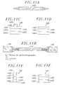
- FIGS. 11A and 11B the configuration before is illustrated resin and nitride removal, respectively after the first photolithography and after the second photolithography.
- the figures 11C and 11D represent vertical section views of the structure respectively at the second section 142 and first section 140, after the first engraving, and FIGS. 11E and 11F represent views similar in vertical sections respectively at the second section 142 and first section 140 after the second etching.
- the guides 14 are formed of substantially rectilinear segments between the lenses 10, 12.
- Each of the first sections 140 of a guide 14 is itself split into two segments 140A, 140B which surround a second section 142.
- the segments 140A and 140B and the section 142 are substantially aligned.
- the section 142 and the segment 140B are substantially aligned while the segment 140A is arranged in oblique, inclined to them.
- connection zones between the second section 142 and respectively each of the segments 140A, 140B are referenced 146, 147.
- this area is in the form of an isosceles triangle according to FIG. 4, the median plane of symmetry of the second sections 142 being perpendicular to the general direction of the guides and the areas of connection being symmetrical with respect to a plane orthogonal to this direction.
- the area of the second sections 142 is in the form of right triangle according to Figure 5, the connection area 146 being tilted on the general direction of the guides while the area of connection 147 is orthogonal to this general direction.
- the devices are long (about lmm), they are formed from a guide of very slight curvature. These guides as well reduce propagation losses compared to a PHASAR classic curved guide structure dependent on the temperature. To facilitate the understanding of straight lines rather than curves are shown in the accompanying figures. In reality, a curvature and a mode adapter are required to reduce loss of connection, between the structures of index n1 and n2, that is to say between the segments 140A, 140B and the second sections 142.
- This junction is shown schematically in Figure 4 and omitted on the FIGS. 5 and 6 to better show the structure of the segments 140A, 140B and second sections 142.
- the two sections 140, 142 can be formed by an end-to-end coupling between a guide 140 composed of semiconductor, for example InP and a polymer resin 142, for example of the type PMMA.
- the variation of the index with the temperature is positive for InP and negative for PMMA.
- K 1 (K always choose positive).
- each second section 142 is the still placed between two segments 140A, 140B of the first section 140.
- each second section 142 is itself split into two rectilinear segments orthogonal to each other 142A, 142B. These second segments 142A, 142B are coupled together by a 45 ° mirror. They are also coupled to a first segment 140A, 140B respective aligned. The mirrors 150 thus ensure the coupling between two similar segments 142A, 142B.
- Figure 9 corresponds to a guide configuration with classic turns in themselves.
- the mirrors 150 can for example be produced according to teaching of the document [6] FR-A-2725040 (patent application French n ° 94 11369).
- independence from polarization can also be set in the same way as for a phasar classic.
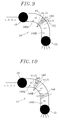
- each guide 14 comprises at least two sections 140, 142 ensuring control of the effects of temperature and at least one third section 144 in series on each guide of variable length from one guide to another in constant step ⁇ L3, ensuring compensation for the polarization, as shown schematically in Figure 10.
- each first section 140 is divided into three segments 140A, 140B, 140C which frame two by two respectively a second section 142 and a third section 144,
- ⁇ L can be negative.
- a example is given by figure 10: ⁇ L3 is of opposite sign to ⁇ L1 since it decreases towards the outside of the turn.
- the accuracy of the above system can be further improved by involving the variation of the length of the guide sections in temperature function.
- the values K1 and K2 are experimental data and contain both the variation of the index and the variation in length with temperature.
Abstract
Description
Le domaine technique de la présente invention est celui de l'optique guidée.The technical field of the present invention is that of guided optics.
La présente invention propose un multiplexeur et/ou démultiplexeur optique utilisable dans le domaine des télécomunications et des capteurs en télémétrie.The present invention provides a multiplexer and / or optical demultiplexer usable in the field of telecommunications and telemetry sensors.
Le dispositif selon l'invention peut constituer un récepteur optique de circuit de réception en détection directe, par exemple pour des systèmes de liaison optique. Un tel dispositif peut être intéressant pour la distribution, pour séparer un ensemble de signaux de longueur d'onde différente arrivant d'une même fibre, vers différents utilisateurs, chacun recevant sa propre longueur d'onde.The device according to the invention can constitute a receiver receiving circuit optics in direct detection, for example for optical link systems. Such a device can be interesting for the distribution, to separate a set of wavelength signals different arriving from the same fiber, to different users, each receiving its own wavelength.
Le dispositif selon l'invention peut aussi être couplé (en hybride ou intégré) avec des lasers ou des ampli-optiques à l'émission.The device according to the invention can also be coupled (in hybrid or integrated) with lasers or optical amplifiers on emission.
Le dispositif selon l'invention est notamment intéressant dans des fonctions commutation, brasseurs et boucle locale. Il pourra être utilisé, également dans des interconnexions optiques entre, par exemple, des "puces" électroniques rapides à haut degré d'intégration ou entre ordinateurs ou à l'intérieur d'ordinateurs.The device according to the invention is particularly advantageous in switching, brewers and local loop functions. It could be used, also in optical interconnections between, for example, fast electronic "chips" with a high degree of integration or between computers or inside computers.
Différentes structures de multiplexeurs et/ou démultiplexeurs optiques ont été décrites dans la littérature.Different structures of multiplexers and / or demultiplexers optics have been described in the literature.
On peut citer par exemple les documents suivants : [1] ECOC 96, Extremely compact 1.31µm-1.55µm phased aray duplexer on InP with -30dB crosstalk over 100nm ; R. Mestric et al., qui décrit la réalisation d'un démultiplexeur à deux longeurs d'onde 1.3µm et 1.55µm ; [2] ECOC 96, Compact low loss 8x10GHz polarisation independent WDM receiver C.A.M. Steenbergen et al. , qui décrit la réalisation d'un démultiplexeur intégré à des détecteurs et propose d'utiliser deux structures de guide pour régler le problème de la polarisation.Examples include the following documents: [1] ECOC 96, Extremely compact 1.31µm-1.55µm phased aray duplexer on InP with -30dB crosstalk over 100nm; R. Mestric et al., Who describes the realization a demultiplexer with two wavelengths 1.3 µm and 1.55 µm; [2] ECOC 96, Compact low loss 8x10GHz independent WDM polarization receiver C.A.M. Steenbergen et al. , which describes the realization of a demultiplexer integrated with detectors and offers to use two guide structures to solve the problem of polarization.
Les (dé)multiplexeurs généralement utilisés de nos jours sont
du type à réseau de guides représenté sur la figure 1 annexée. Ces
démultiplexeurs sont composés de deux dioptres plans 10, 12 séparés par un
réseau 14 de guides. La différence de marche ΔL entre deux guides
consécutifs 14 est constante et permet le déphasage et donc le
démultiplexage. Sur la figure 1, P1 représente le plan équiphase pour un
signal d'entrée tandis que P2 représente le plan équiphase pour un signal
venant d'une des sorties.The (de) multiplexers generally used today are
of the type with guide network shown in FIG. 1 attached. These
demultiplexers are composed of two
Les dispositifs multiplexeurs/démultiplexeurs connus ainsi proposés ont déjà rendu de grands services. Cependant, ils ne donnent pas totalement satisfaction.Known multiplexer / demultiplexer devices as well offered have already rendered great services. However, they do not give totally satisfied.
L'inconvénient principal de ces dispositifs connus est leur forte dépendance avec la température, intrinsèque au matériau utilisé.The main drawback of these known devices is their strong dependence on temperature, intrinsic to the material used.
En effet, l'indice du matériau varie en fonction de la température et ainsi la différence de marche entre deux guides consécutifs est modifiée avec la température et entraíne un déplacement des pics se décallant par rapport aux guides de sortie.Indeed, the index of the material varies according to the temperature and thus the path difference between two guides changes with the temperature and causes displacement peaks shifting relative to the outlet guides.
Le matériau SiO2 possède un faible coefficient de variation de l'indice avec la température (cette variation entraíne un décallage d'environ 1nm pour 100°C). Cependant, ce matériau est limité au niveau de l'intégration monolithique (sur le même matériau) de dispositifs tel que les lasers, les amplificateurs optiques ou les détecteurs.The SiO2 material has a low coefficient of variation of the index with the temperature (this variation leads to an offsetting about 1nm for 100 ° C). However, this material is limited to the level of monolithic integration (on the same material) of devices such as lasers, optical amplifiers or detectors.
En revanche, l'intégration monolithique permettant de réduire les coûts de production (par rapport à l'hybridation sur différents matériaux) est possible sur InP. Mais les variations de l'indice en fonction de la température pour l'InP sont considérables (cette variation induit un décallage d'environ 1nm pour 10°C). La publication [3] Polarisation independent 8x8 waveguide grating multiplexer on InP Electronics Letters, Jan. 21, 1993, vol. 29, n° 2 ; M. Zirngibl et al., donne une variation de 1,5nm/10°C. Cette forte dépendance exige un contrôle de la température à l'aide de moyens externes au dispositif, par exemple sous forme d'un élément à effet Peltier, augmentant les coûts de réalisation.On the other hand, the monolithic integration allowing to reduce production costs (compared to hybridization on different materials) is possible on InP. But the variations in the index as a function of the temperature for InP are considerable (this variation induces a about 1nm of offset for 10 ° C). The publication [3] Polarization independent 8x8 waveguide grating multiplexer on InP Electronics Letters, Jan. 21, 1993, vol. 29, no. 2; M. Zirngibl et al., Gives a variation 1.5nm / 10 ° C. This heavy dependence requires temperature control using means external to the device, for example in the form of a Peltier effect element, increasing production costs.
Bien entendu, dans le cas d'un démultiplexeur large raie avec un faible nombre de raies, tel que le duplexeur 2 raies de la référence [1] ECOC 96 avec des raies de 100nm, la température ne perturbe pas le démultiplexage ou très peu. Par contre, dans le cas d'une application multilongueur d'onde et des raies de 0.65nm, l'instabilité en température doit être contrôlée.Of course, in the case of a wide line demultiplexer with a low number of lines, such as the 2-line duplexer of the reference [1] ECOC 96 with 100nm lines, the temperature does not disturb the demultiplexing or very little. However, in the case of an application 0.65nm multi-wavelength and lines, temperature instability must be checked.
La présente invention a pour but de proposer un dispositif qui permet de réduire et/ou d'annuler l'effet de la température sur un dispositif de (dé)multiplexage sans aucune action extérieure au dispositif et quel que soit le matériau utilisé (SiO2, InP, polymère, Al2O3, LiNbO3 ...). The object of the present invention is to propose a device which reduces and / or cancels the effect of temperature on a (de) multiplexing device without any action external to the device and whatever the material used (SiO2, InP, polymer, Al2O3, LiNbO3 ...).
Accessoirement la présente invention a pour but de proposer un dispositif adapté soit pour réduire l'effet de la température, soit augmenter cet effet pour offrir un moyen de contrôle du signal, par la température sur le canal désiré. L'invention permet ainsi une plus grande tolérance sur la géométrie du dispositif.Incidentally, the present invention aims to propose a device adapted either to reduce the effect of temperature or increase this effect to provide a means of signal control, by temperature on the desired channel. The invention thus allows greater tolerance on the geometry of the device.
L'annulation de l'effet de la température permet de s'affranchir d'un dispositif de régulation externe.Canceling the effect of temperature allows get rid of an external regulation device.
Les buts précités sont atteints dans le cadre de la présente invention grâce à un dispositif formant multiplexeur et/ou démultiplexeur optique du type comprenant deux zones non guidées latéralement agissant comme des lentilles dans le plan, séparées par un réseau de guides possédant des différences de longueur contrôlées, caractérisé par le fait que chaque guide comprend au moins deux tronçons placés en série et possédant des longueurs et des indices de réfraction respectifs adaptés pour contrôler l'influence de variations de la température sur le dispositif, c'est à dire pour contrôler la position de sortie des différentes longueurs d'onde du dispositif dépendant des fluctuations de température.The aforementioned goals are achieved within the framework of this invention by means of a multiplexer device and / or optical demultiplexer of the type comprising two unguided zones laterally acting as lenses in the plane, separated by a network of guides with controlled length differences, characterized in that each guide comprises at least two sections placed in series and having lengths and indices of refraction respective adapted to control the influence of variations in the temperature on the device, i.e. to control the position of output of the different wavelengths of the device depending on the temperature fluctuations.
Selon un premier mode de réalisation conforme à la présente invention, les variations d'indice de réfraction avec la température évoluent dans le même sens pour les matériaux composant les deux tronçons de chaque guide respectif et chacun de ces deux tronçons possèdent des longueurs respectives qui évoluent en sens inverse, d'un guide à l'autre.According to a first embodiment in accordance with this invention, variations in refractive index with temperature move in the same direction for the materials making up the two sections of each respective guide and each of these two sections have respective lengths which move in opposite directions, from a guide to the other.
Selon un second mode de réalisation conforme à la présente invention, les variations d'indice de réfraction avec la température évoluent dans des sens opposés pour les matériaux composant les deux tronçons de chaque guide respectifs et chacun de ces deux tronçons possèdent des longueurs respectives qui évoluent dans le même sens, d'un guide à l'autre.According to a second embodiment in accordance with this invention, variations in refractive index with temperature evolve in opposite directions for the materials making up the two sections of each respective guide and each of these two sections have respective lengths which move in the same direction, from a guide to the other.
La présente invention propose ainsi un (dé)multiplexeur soit indépendant de la température, soit de dépendance (dλ/dT) choisie et désirée en fonction de la température.The present invention thus provides a (de) multiplexer either independent of temperature, either of dependence (dλ / dT) chosen and desired depending on the temperature.
D'autres caractéristiques, buts et avantages de l'invention apparaítront à la lecture de la description détaillée qui va suivre, et en regard des dessins annexés, donnés à titre d'exemples non limitatifs et sur lesquels :
- la figure 1 précédemment décrite illustre schématiquement la structure générale d'un démultiplexeur conforme à l'état de la technique,
- les figures 2 et 3 représentent des vues en coupe verticale de deux tronçons de guide conformes à l'invention,
- les figures 4, 5 et 6 représentent des vues schématiques de dessus de trois variantes de structures de dispositif conformes à un mode de réalisation principal de l'invention,
- les figures 7, 8 et 9 représentent des vues schématiques de dessus de trois variantes de structure de dispositif conformes à un second mode de réalisation principal de l'invention,
- la figure 10 représente une vue schématique de dessus d'une variante de structure possédant une compensation additionnelle à la polarisation,
- les figures 11A et 11B illustrent schématiquement deux étapes de gravure pour l'obtention de tronçons avec adaptateur de mode conformes à la présente invention et les figures 11C et 11D représentent des vues en coupes verticales de la structure respectivement au niveau des second tronçon et premier tronçon, après la première gravure, tandis que les figures 11E et 11F représentent des vues similaires en coupes verticales respectivement au niveau des second tronçon et premier tronçon après la seconde gravure.
- FIG. 1 previously described schematically illustrates the general structure of a demultiplexer according to the state of the art,
- FIGS. 2 and 3 represent views in vertical section of two sections of guide in accordance with the invention,
- FIGS. 4, 5 and 6 represent schematic views from above of three variants of device structures in accordance with a main embodiment of the invention,
- FIGS. 7, 8 and 9 represent schematic views from above of three variants of the device structure in accordance with a second main embodiment of the invention,
- FIG. 10 represents a schematic top view of a variant structure having additional polarization compensation,
- FIGS. 11A and 11B schematically illustrate two etching steps for obtaining sections with mode adapter in accordance with the present invention and FIGS. 11C and 11D represent views in vertical sections of the structure respectively at the level of the second section and first section , after the first etching, while FIGS. 11E and 11F show similar views in vertical sections respectively at the level of the second section and first section after the second etching.
Comme indiqué précédemment, l'invention concerne les
dispositifs formant multiplexeur et/ou démultiplexeur optique du type
comprenant deux lentilles intégrées 10, 12 placées par exemple l'une
devant un guide d'entrée et l'autre devant plusieurs guides de sortie, ou
inversement l'une devant plusieurs guide d'entrée et l'autre devant un
guide de sortie, lesdites lentilles intégrées 10, 12 étant en outre placées
entre un réseau ou nappe de guides 14 présentant deux à deux des
différences de marche ΔL contrôlées. L'invention propose plus
précisément une structure permettant de contrôler l'influence de la
température sur un tel dispositif.As indicated above, the invention relates to
optical multiplexer and / or demultiplexer devices of the type
comprising two integrated
L'invention repose sur l'analyse suivante.The invention is based on the following analysis.
L'équation donnant la longueur d'onde centrale d'un
démultiplexeur de type PHASAR comprenant une série de guides optiques
placés entre deux dioptres plans, est la suivante : λ=nΔL/m dans laquelle n
représente l'indice effectif du guide utilisé dans la nappe de guides 14, ΔL
représente la différence de chemin optique entre deux guides consécutifs
et m représente l'ordre d'interférence.The equation giving the central wavelength of a
PHASAR type demultiplexer comprising a series of optical guides
placed between two planar diopters, is as follows: λ = nΔL / m in which n
represents the effective index of the guide used in the
La variation de longueur d'onde en fonction de la température
est donc par dérivation :
Afin de simplification, on suppose pour l'instant que le terme dn/dT contient aussi le terme de variation de la longueur; en fait dn/dT → (dn/dT) + (ndΔL/ΔLdT).For the sake of simplification, it is assumed for the moment that the term dn / dT also contains the term variation of the length; actually dn / dT → (dn / dT) + (ndΔL / ΔLdT).
Pour obtenir une indépendance (totale ou partielle) en température, le dispositif conforme à la présente invention possède au niveau de chaque guide au moins deux tronçons de guide placés en série et possédant des longueurs et des indices effectifs de réfraction respectifs adaptés.To obtain independence (total or partial) in temperature, the device according to the present invention has at level of each guide at least two sections of guide placed in series and having respective lengths and effective indices of refraction adapted.
Sur les figures et suivantes annexées, ces deux tronçons en
série sont références 140, 142.In the attached figures and following, these two sections in
series are
Plus précisément encore la présente invention propose deux modes de réalisation principaux.Even more precisely, the present invention proposes two main embodiments.
Dans le premier mode de réalisation, les variations d'indice de
réfraction avec la température évoluent dans le même sens pour les
matériaux composant les deux tronçons 140, 142 de chaque guide 14
respectif, mais chacun de ces deux tronçons 140, 142 possèdent des
longueurs respectives qui évoluent en sens inverse, d'un guide à l'autre.In the first embodiment, the variations in the index of
refraction with temperature evolve in the same direction for
materials making up the two
Les figures 4, 5 et 6 représentent trois variantes d'un tel dispositif.Figures 4, 5 and 6 show three variants of such device.
L'équation donnant la longueur d'onde centrale λ en fonction
de la différence de chemin entre deux guides consécutifs d'une telle
structure est la suivante :
Le démultiplexeur est conçu tel que ΔL2=KΔL1 avec k=(dn1/dT)/(dn2/dT)=K1/K2>0 c'est-à-dire des variations d'indice de réfraction avec la température dans le même sens pour les deux matériaux composant les deux tronçons en série, si l'on veut annuler les effets de la température.The demultiplexer is designed such that ΔL2 = KΔL1 with k = (dn1 / dT) / (dn2 / dT) = K1 / K2> 0 i.e. variations in the index of refraction with temperature in the same direction for the two materials composing the two sections in series, if we want to cancel the effects of temperature.
Par ailleurs, pour avoir ΔL1 suffisamment petit pour un phasar de faible dimension, n1-Kn2 doit être suffisamment grand.Furthermore, to have ΔL1 small enough for a phasar small, n1-Kn2 must be large enough.
Dans le second mode de réalisation, les variations d'indice de
réfraction avec la température évoluent dans des sens opposés pour les
matériaux composant les deux tronçons 140, 142 de chaque guide 14
respectif et chacun de ces deux tronçons 140, 142 possède des longueurs
respectives qui évoluent dans le même sens, d'un guide à l'autre.In the second embodiment, the variations in the index of
refraction with temperature evolve in opposite directions for
materials making up the two
Les figures 7, 8 et 9 représentent trois variantes d'un tel dispositif.Figures 7, 8 and 9 show three variants of such device.
L'équation donnant la longueur d'onde centrale λ en fonction
de la différence de chemin entre deux guides consécutifs d'une telle
structure est la suivante :
Le démultiplexeur est alors conçu tel que ΔL2=KΔL1 avec K=-(dn1/dT)/(dn2/dT)>0 c'est-à-dire des variations de l'indice de réfraction avec la température dans le sens opposé pour les deux matériaux composant les tronçons en série, si l'on veut annuler les effets de la température.The demultiplexer is then designed such that ΔL2 = KΔL1 with K = - (dn1 / dT) / (dn2 / dT)> 0 i.e. variations of the index of refraction with temperature in the opposite direction for both materials composing the sections in series, if we want to cancel the effects of the temperature.
Dans ce cas, le facteur n1+Kn2 tiré de mλ=(n1+Kn2)ΔL1 est suffisamment grand pour avoir ΔL1 suffisamment petit permettant de réaliser un phasar de faible dimension.In this case, the factor n1 + Kn2 taken from mλ = (n1 + Kn2) ΔL1 is large enough to have ΔL1 small enough to realize a phasar of small dimension.
La variation de la longueur d'onde pour les deux géométries
précitées est la suivante :
Pour ΔL2=KΔL1, mdλ/dT=0.For ΔL2 = KΔL1, mdλ / dT = 0.
Ainsi nous obtenons l'indépendance vis à vis de la température avec ΔL2=KΔL1.So we get independence from temperature with ΔL2 = KΔL1.
Pour disposer d'une dépendance avec la température différente de celle donnée par les matériaux et déterminée au préalable, il suffit d'agir sur la géométrie du PHASAR en modifiant le rapport ΔL2/ΔL1 qui pourra être supérieur ou inférieur à K.To have a dependence on the different temperature of that given by the materials and determined beforehand, it suffices to act on the geometry of the PHASAR by modifying the ratio ΔL2 / ΔL1 which may be greater or less than K.
On va maintenant décrire des exemples conformes au premier
mode de réalisation précité pour lequel les variations d'indice avec la
température sont de même sens pour les deux matériaux composant
respectivement les deux tronçons en série 140, 142 de chaque guide
consécutif 14.We will now describe examples conforming to the first
aforementioned embodiment for which the variations in index with the
temperature are the same direction for the two component materials
respectively the two sections in
De l'équation (1) on déduit mλ=(n1-Kn2)ΔL1.From equation (1) we deduce mλ = (n1-Kn2) ΔL1.
Dans ces exemples les deux tronçons en série 140, 142 sont
formés de structures sur substrat InP, composées de deux empilements de
couches différentes pour réaliser les deux tronçons de guides. Ces deux
structures sont illustrées respectivement sur les figures 2 et 3 annexées.In these examples the two sections in
Plus précisément encore, selon un mode de réalisation
particulier, le premier tronçon 140 est composé de trois fines couches 1400
(500Å) de quaternaire GalnAsP(gap de 1.3µm) séparées de couches 1402
d'lnP d'une épaisseur de 0.55µm. Ce premier tronçon 140 est réalisé par
gravure (voir figure 2) pour définir un ruban de largeur 5µm. Le second
tronçon 142 est constitué d'un guide quaternaire 1420 GalnAsP
(gap=1.3µm) surmonté d'une couche 1422 d'lnP obtenu par gravure RIE de
largeur 2µm. Le transfert du mode d'une structure de guide 140 à l'autre
142 se fait par un adaptateur de mode.More precisely still, according to an embodiment
particular, the
Un tel adaptateur de mode peut être par exemple conforme aux enseignements du document [4] FR-A-2732777 (demande de brevet français n° 95 04031).Such a mode adapter can for example conform to lessons from document [4] FR-A-2732777 (French patent application n ° 95 04031).
L'indice effectif n1 de la première structure 140 est d'environ
3.19 et celui n2 de la seconde structure 142 est de 3.21. Les variations
d'indice avec la température sont K1=0.127nm/°C pour la première
structure 140 et pour la seconde structure 142, K2=0.15nm/°C. K2>K1
puisque le gap 1.3µm de la structure 142 est plus proche de la longueur
d'onde 1.54µm que ne l'est le gap équivalent de 0.919µm de la structure 140.
On peut supposer qu'au premier ordre la variation d'indice effectif du
mode guidé avec T est équivalente à celle du matériau de coeur de guide.
Ainsi n1-Kn2=0.47. Pour une longueur d'onde de 1.54µm avec une largeur
de fenêtre autour de cette valeur d'environ 30nm, l'ordre m est de
1540/30=50. Nous obtenons pour ΔL1 une valeur de 164µm. Ceci représente
une longueur minimale pour la nappe de 40 guides de 164x40=6560µm.The effective index n1 of the
On notera que selon l'illustration schématique des figures 2 et 3,
la seconde structure 142 formée des couches 1420, 1422 est réalisée au-dessus
de la première structure composée des couches 1400 et 1402.Note that according to the schematic illustration of FIGS. 2 and 3,
the
On va maintenant décrire un procédé particulier de réalisation de ces structures, et notamment leurs adaptateurs de mode.We will now describe a particular method of production of these structures, and in particular their mode adapters.
L'adaptateur de mode permettant le passage sans pertes d'énergie d'un guide à l'autre est réalisé grâce à deux masques :
- un premier masque permet la réalisation du ruban 142 de 2µm de largeur
avec deux pointes à chaque extrémité comme illustré sur les figures 11A,
11C et 11D, par une gravure des couches supérieures
InP 1422et GalnAsP 1420 au dessus de lastructure tricouche 1400et 1402, sur les zones destinées à former le ruban 142 (voir figure 11C) et élimination complète descouches InP 1422et GalnAsP 1420 en dehors des zones précitées, y compris sur les zones destinées à former le tronçon 140 (voir figure 11D). - un deuxième masque : le SiNx du 1er ruban 142 est conservé et le protège pour la deuxième gravure assurant la réalisation du tronçon 140 tout en terminant le tronçon 142 par gravure de la structure tricouche (voir figures 11E et 11F).
- a first mask enables the
ribbon 142 2 μm wide to be produced with two points at each end as illustrated in FIGS. 11A, 11C and 11D, by etching theupper layers InP 1422 andGalnAsP 1420 above the three-layer structure InP 1422 andGalnAsP 1420 layers outside the aforementioned zones, including on the zones intended to form the section 140 (see FIG. 11D). - a second mask: the SiNx of the
1st ribbon 142 is preserved and protects it for the second etching ensuring the production of thesection 140 while finishing thesection 142 by etching of the three-layer structure (see FIGS. 11E and 11F).
Sur les figures 11A et 11B, on a illustré la configuration avant
retrait de la résine et du nitrure, respectivement après la première
photolithographie et après la deuxième photolithographie. Les figures
11C et 11D représentent des vues en coupes verticales de la structure
respectivement au niveau des second tronçon 142 et premier tronçon 140,
après la première gravure, et les figures 11E et 11F représentent des vues
similaires en coupes verticales respectivement au niveau des second
tronçon 142 et premier tronçon 140 après la seconde gravure.In FIGS. 11A and 11B, the configuration before is illustrated
resin and nitride removal, respectively after the first
photolithography and after the second photolithography. The figures
11C and 11D represent vertical section views of the structure
respectively at the
Pour la définition du deuxième ruban 140 de 5µm de large, il
n'est pas prévu de protection de la résine du ruban 142 pour faciliter
l'alignement avec le premier ruban 142. C'est ainsi que l'on aura réalisé
au préalable un premier nitrure suffisamment épais pour protéger le
ruban 142 puisqu'une partie de celui-ci sera gravée après la deuxième
photolithographie.For the definition of the second 140 strip 5µm wide, it
protection of the
Les figures 4, 5 et 6 représentent deux cas conformes au
premier mode de réalisation de la présente invention : le cas où K=1
(ΔL1=ΔL2) avec deux types de triangle délimitant la zone des seconds
tronçons 142 et permettant le déphasage (figures 4 et 5) et le cas où K#1
(figure 6).Figures 4, 5 and 6 show two cases in accordance with
first embodiment of the present invention: the case where K = 1
(ΔL1 = ΔL2) with two types of triangle delimiting the area of the
Selon les trois variantes illustrées sur les figures 4, 5, 6 les
guides 14 sont formés de segments sensiblement rectilignes entre les
lentilles 10, 12.According to the three variants illustrated in Figures 4, 5, 6 the
Chacun des premiers tronçons 140 d'un guide 14 est lui-même
scindé en deux segments 140A, 140B qui encadrent un second tronçon 142.Each of the
Selon les figures 4 et 5, les segments 140A et 140B et le tronçon
142 sont sensiblement alignés.According to FIGS. 4 and 5, the
En revanche, selon la figure 6, le tronçon 142 et le segment
140B sont sensiblement alignés tandis que le segment 140A est disposé en
oblique, incliné par rapport à ceux-ci.On the other hand, according to FIG. 6, the
Les zones de raccordement entre le second tronçon 142 et
respectivement chacun des segments 140A, 140B sont référencées 146, 147.The connection zones between the
Les variations de longueur des seconds tronçons 142 évoluant
en sens inverse de la somme des longueurs des segments 140A, 140B, d'un
guide à l'autre, et ce avec des pas constants d'un guide donné au suivant,
la zone délimitée par l'ensemble des seconds tronçons 142 entre les deux
segments respectifs 140A, 140B est de forme générale triangulaire.The variations in length of the
Plus précisément, cette zone est en forme de triangle isocèle
selon la figure 4, le plan médian de symétrie des seconds tronçons 142
étant perpendiculaire à la direction générale des guides et les zones de
raccordement étant symétriques par rapport à un plan orthogonal à cette
direction.More precisely, this area is in the form of an isosceles triangle
according to FIG. 4, the median plane of symmetry of the
En revanche, la zone des seconds tronçons 142 est en forme de
triangle rectangle selon la figure 5, la zone de raccordement 146 étant
inclinée sur la direction générale des guides tandis que la zone de
raccordement 147 est orthogonale à cette direction générale.On the other hand, the area of the
Bien entendu des variantes intermédiaires de ces deux dispositions particulières illustrées sur les figures 4 et 5 peuvent être retenues, en respectant ΔL1=ΔL2.Of course intermediate variants of these two particular arrangements illustrated in Figures 4 and 5 can be retained, respecting ΔL1 = ΔL2.
L'homme de l'art comprendra aisément à l'examen de la figure
6 que la variante illustrée sur cette figure permet d'obtenir ΔL1<ΔL2. C'est-à-dire
que la variation de longueur ΔL2 des seconds tronçons 142, d'un
guide 14 à l'autre, évoluent toujours en sens inverse mais avec une
amplitude différente de la variation ΔL1 de la somme des longueurs des
segments 140A, 140B. L'angle entre la direction des segments de guide
140A, en sortie du premier dioptre plan 10 et la direction des segments de
guide 140B en entrée du second dioptre plan 12 détermine directement le
rapport ΔL1/ΔL2.Those skilled in the art will readily understand on examining the figure
6 that the variant illustrated in this figure makes it possible to obtain ΔL1 <ΔL2. That is to say
that the variation in length ΔL2 of the
Il est à noter que bien que les dispositifs sont longs (environ
lmm), ils sont formés de guide de très faible courbure. Ces guides ainsi
permettent de réduire les pertes de propagation par rapport à une
structure à guide incurvé classique du PHASAR dépendant de la
température. Pour faciliter la compréhension des droites plutôt que des
courbes sont représentées sur les figures annexées. En réalité, une
courbure et un adaptateur de mode s'imposent pour réduire les pertes de
raccordement, entre les structures d'indice n1 et n2, c'est-à-dire entre les
segments 140A, 140B et les seconds tronçons 142.Note that although the devices are long (about
lmm), they are formed from a guide of very slight curvature. These guides as well
reduce propagation losses compared to a
PHASAR classic curved guide structure dependent on the
temperature. To facilitate the understanding of straight lines rather than
curves are shown in the accompanying figures. In reality, a
curvature and a mode adapter are required to reduce loss of
connection, between the structures of index n1 and n2, that is to say between the
Par ailleurs sur les trois schémas des figures 4, 5 et 6, la
jonction entre les guides 14 de la nappe et chaque dioptre plan 10, 12
représenté par un disque, n'est pas représentée dans le détail pour éviter
d'alourdir les figures.Furthermore, in the three diagrams of FIGS. 4, 5 and 6, the
junction between the
Cette jonction est schématisée sur la figure 4 et omise sur les
figures 5 et 6 pour faire mieux apparaitre la structure des segments 140A,
140B et des seconds tronçons 142.This junction is shown schematically in Figure 4 and omitted on the
FIGS. 5 and 6 to better show the structure of the
On va maintenant décrire des exemples conformes au second
mode de réalisation de l'invention pour lequel les variations d'indice avec
la température sont de sens opposés pour les deux matériaux composant
respectivement les deux tronçons en série 140, 142 de chaque guide 14, en
regard des figures 7, 8 et 9.We will now describe examples in accordance with the second
embodiment of the invention for which the index variations with
the temperature are in opposite directions for the two component materials
respectively the two sections in
De l'équation 2, on déduit : mλ=(n1+Kn2)ΔL1.From
Dans ce cas les deux tronçons 140, 142 peuvent être formés par
un couplage bout à bout entre un guide 140 composé de semi-conducteur,
par exemple d'InP et une résine 142 de polymère, par exemple de type
PMMA.In this case the two
La variation de l'indice avec la température est positive pour l'InP et négative pour le PMMA.The variation of the index with the temperature is positive for InP and negative for PMMA.
Pour la partie 140 InP, on peut choisir le guide de la structure décrite précédemment en regard de la figure 2.For the 140 InP part, you can choose the structure guide previously described with reference to FIG. 2.
Le guide 142 en PMMA peut être conforme aux enseignements
du document [5] Integration of a Laser Diode with a Polymer-Based
Waveguide for Photonic Integrated Circuits N. Bonadma et al., IEEE
Photonics Technology Letters, Vol. 6, n° 10, Oct. 1994.
L'indice effectif n1 de la première structure 140 est d'environ
3.18, celui n° 2 de la seconde structure 142 de 1.5 environ. Les variations
d'indice avec la température sont équivalentes mais opposées d'où K=1 (K
choisi toujours positif). L'équation s'écrit : mλ=(n1+n2)ΔL1. Pour une
longueur d'onde de 1.54µm, avec une largeur de fenêtre autour de cette
valeur d'environ 30nm, l'ordre m devra être de 1540/30=50. Avec une
somme d'indice de 4.68, nous obtenons pour ΔL1 une valeur de 16.4µm.The effective index n1 of the
On a illustré sur les figures 7, 8 et 9 trois géométries de PHASAR répondant au second mode de réalisation, en accord avec la différence de marche (n1+n2) ΔL1.We illustrated in Figures 7, 8 and 9 three geometries of PHASAR corresponding to the second embodiment, in agreement with the difference of on (n1 + n2) ΔL1.
On a schématisé sur la figure 7 une géométrie dans laquelle les
deux tronçons 140, 142 sont formés de guides rectilignes orthogonaux
entre eux et d'écart constant entre guides adjacents, raccordés
respectivement aux dioptres plans 10, 12, d'une part et raccordés d'autre
part entre eux grâce à des miroirs 150 à 45°. On comprend que ΔL1=ΔL2 si
l'écartement entre les guides 140 est identique à celui des guides 142.
L'angle entre les deux tronçons 140 et 142 (qui peut être différent de 90°)
et l'écart ou entre-axe entre les tronçons 140, 142 déterminent
directement la valeur de ΔL1 et ΔL2 et permettent d'obtenir ΔL1≠ΔL2.
Cependant une telle structure avec miroir à 45° pour assurer le couplage
entre deux tronçons de guide 140, 142 de natures différentes est difficile à
réaliser et à exploiter.We have schematized in Figure 7 a geometry in which the
two
On préfère en effet, comme illustré sur les figures 8 et 9, opérer
le raccordement entre les tronçons 140, 142 sur des parties de guide
sensiblement rectilignes. It is indeed preferred, as illustrated in FIGS. 8 and 9, to operate
the connection between the
Ainsi selon les figures 8 et 9 chaque second tronçon 142 est la
encore placé entre deux segments 140A, 140B du premier tronçon 140.Thus according to FIGS. 8 and 9, each
Plus précisément, selon la figure 8, chaque second tronçon 142
est lui-même scindé en deux segments rectilignes orthogonaux entre eux
142A, 142B. Ces seconds segments 142A, 142B sont couplés entre eux par un
miroir à 45°. Ils sont par ailleurs couplés à un premier segment 140A, 140B
respectif aligné. Les miroirs 150 assurent ainsi le couplage entre deux
segments de même nature 142A, 142B.More precisely, according to FIG. 8, each
La figure 9 correspond à une configuration de guide avec des virages classiques en soi.Figure 9 corresponds to a guide configuration with classic turns in themselves.
Les miroirs 150 peuvent par exemple être réalisés selon
l'enseignement du document [6] FR-A-2725040 (demande de brevet
français n° 94 11369).The
Sur la figure 9, le plan équiphase en partant de l'entrée est référencé P1, celui en partant de la sortie est référencé P2.In Figure 9, the equiphase plan from the entrance is referenced P1, the one starting from the output is referenced P2.
Dans la description qui précède, la dépendance à la polarisation a été ignorée.In the above description, the dependence on polarization has been ignored.
Cependant, dans le cadre du (dé)multiplexeur indépendant de la température, conforme à l'invention, l'indépendance à la polarisation peut également être réglée de la même façon que pour un phasar classique.However, in the context of the independent (de) multiplexer of the temperature, according to the invention, independence from polarization can also be set in the same way as for a phasar classic.
Pour cela, on peut citer au moins trois méthodes :
- travailler à un ordre différent pour le TE et pour le TM. Cette méthode réduit la taille de la fenêtre en longueur d'onde et limite le nombre de canaux.
- utiliser un guide de structure carré pour un indice TE et TM identique. Dans le cas de l'invention, la biréfringence du tronçon 140 de guide doit être égale à celle du tronçon 142 de guide. Pour les phasars classiques de la littérature un seul guide nonbiréfringent est utilisé. Cette méthode est très peu tolérante au niveau de la géométrie induisant des difficultés de fabrication.
- utiliser un tronçon de guide additionnel sur chaque
guide 14, pour compenser les différences de polarisation.
- work in a different order for the TE and for the TM. This method reduces the window size in wavelength and limits the number of channels.
- use a square structure guide for an identical TE and TM index. In the case of the invention, the birefringence of the
guide section 140 must be equal to that of theguide section 142. For the classic phasars of the literature, a single non-birefringent guide is used. This method is very tolerant at the level of the geometry inducing manufacturing difficulties. - use an additional guide section on each
guide 14, to compensate for differences in polarization.
Cette méthode pourra être inspirée des enseignements du document [7] Démultiplexeur Intégré sur InP indépendant de la polarisation A. Rigny et al. JNOG 96, lui-même basé sur le document [4] FR-A-2732777.This method could be inspired by the teachings of the document [7] Integrated demultiplexer on InP independent of polarization A. Rigny et al. JNOG 96, itself based on document [4] FR-A-2732777.
Dans ce cas chaque guide 14 comprend au moins deux tronçons
140, 142 assurant un contrôle des effets de la température et au moins un
troisième tronçon 144 en série sur chaque guide d'une longueur variable
d'un guide à l'autre par pas constant ΔL3, assurant une compensation de la
polarisation, comme schématisé sur la figure 10.In this case each
Plus précisément encore selon cette figure 10, chaque premier
tronçon 140 est scindé en trois segments 140A, 140B, 140C qui encadrent
deux à deux respectivement un second tronçon 142 et un troisième tronçon
144,More precisely still according to this figure 10, each
Là encore, le plan équiphase en partant de l'entrée est référencé P1 tandis que le plan équiphase en partant de la sortie est référencé P2.Again, the equiphase plan from the entrance is referenced P1 while the equiphase plane from the exit is referenced P2.
Pour déterminer les variations de longueurs ΔL1, ΔL2, ΔL3 entre
les tronçons concernés 140, 142, 144, d'un guide à l'autre, il suffit de
résoudre le système de trois équations à trois inconnues suivant :
Le tronçon i, avec i = 1, 2, 3, est caractérisé par son indice ni, sa différence d'indice (biréfringence) entre deux polarisations Δni et son coefficient thermique Ki faisant intervenir à la fois la variation de l'indice avec la température et la variation de longueur.The section i, with i = 1, 2, 3, is characterized by its index ni, its difference in index (birefringence) between two polarizations Δni and its thermal coefficient Ki involving both the variation of the index with the temperature and the variation in length.
dλ/dT = Cte, cette constante peut être choisie nulle si l'on ne veut pas d'action de la température sur les longueurs d'onde.dλ / dT = Cte, this constant can be chosen null if one does not wants no action of the temperature on the wavelengths.
Dans la résolution du système, des ΔL peuvent être négatifs. Un exemple est donné par la figure 10 : ΔL3 est de signe opposé à ΔL1 puisqu'elle va en décroissant vers l'extérieur du virage.In the system resolution, ΔL can be negative. A example is given by figure 10: ΔL3 is of opposite sign to ΔL1 since it decreases towards the outside of the turn.
La précision du système précité peut être encore améliorée en faisant intervenir la variation de la longueur des tronçons de guide en fonction de la température.The accuracy of the above system can be further improved by involving the variation of the length of the guide sections in temperature function.
Cette variation est donnée dans le document ECOC 96 (3.144)
température indépendant narrow band filter by athermal waveguide,
Yasuo Kokuburn et al. :
Dans ce cas, le système d'équation précité, s'écrit :
La deuxième équation se s'implifie ainsi :
Pour les variantes faisant intervenir uniquement des matériaux semi-conducteurs (premier mode de réalisation notament), les valeurs K1 et K2 sont des données expérimentales et contiennent à la fois la variation de l'indice et la variation de la longueur avec la température.For variants involving only materials semiconductors (first embodiment in particular), the values K1 and K2 are experimental data and contain both the variation of the index and the variation in length with temperature.
Pour les cas faisant intervenir des polymères, les équations se résolvent de la même façon mais en prenant un K1 négatif (ou nul si la variation de la longueur du substrat compense celle de l'indice du guide, voir publication de Kokuburn ECOC96).For cases involving polymers, the equations are solve in the same way but taking a negative K1 (or zero if the variation of the length of the substrate compensates for that of the index of the guide, see publication of Kokuburn ECOC96).
En conclusion, l'utilisation de trois matériaux et/ou structures de guide différents telle que proposée dans le cadre de l'invention permet de régler les problèmes de température et de dépendance à la polarisation dans un (dé)multiplexeur de type PHASAR.In conclusion, the use of three materials and / or structures different guide as proposed in the context of the invention allows to solve the problems of temperature and dependence on polarization in a PHASAR type (de) multiplexer.
Bien entendu, la présente invention n'est pas limitée aux modes de réalisation précédemment décrits, mais s'étend à toute variante conforme à son esprit.Of course, the present invention is not limited to the modes described above, but extends to any variant conforms to his spirit.
Claims (22)
ΔL2=KΔL1
K≠(dn1/dT)/(dn2/dT).Device according to one of claims 1, 2 or 5, characterized in that the variations in lengths ΔL1 and ΔL2 of the sections (140, 142) from one guide (14) to the other and the indices n1, n2 corresponding are adapted to respect relationships:
ΔL2 = KΔL1
K ≠ (dn1 / dT) / (dn2 / dT).
ΔL2=KΔL1
K=-(dn1/dT)/(dn2/dT),
pour annuler les effets de la température.Device according to one of claims 1, 3, 4 and 5, characterized in that the variations in length ΔL1 and ΔL2 of the two sections (140, 142) from one guide (14) to the other and the indices n1 , corresponding n2 have the following relationships:
ΔL2 = KΔL1
K = - (dn1 / dT) / (dn2 / dT),
to cancel the effects of temperature.
K≠-(dn1/dT)/(dn2/dT).Device according to one of claims 1, 3 and 5, characterized in that the variations in length ΔL1 and ΔL2 of the two sections (140, 142) and the corresponding indices n1, n2 correspond to the relationships: ΔL2 = KΔL1
K ≠ - (dn1 / dT) / (dn2 / dT).
Applications Claiming Priority (2)
| Application Number | Priority Date | Filing Date | Title |
|---|---|---|---|
| FR9615855 | 1996-12-23 | ||
| FR9615855A FR2757722B1 (en) | 1996-12-23 | 1996-12-23 | TEMPERATURE INDEPENDENT OPTICAL MULTIPLEXER AND / OR DEMULTIPLEXER |
Publications (1)
| Publication Number | Publication Date |
|---|---|
| EP0851252A1 true EP0851252A1 (en) | 1998-07-01 |
Family
ID=9499003
Family Applications (1)
| Application Number | Title | Priority Date | Filing Date |
|---|---|---|---|
| EP97403114A Withdrawn EP0851252A1 (en) | 1996-12-23 | 1997-12-22 | Temperature independent optical multiplexer and/or demultiplexer |
Country Status (4)
| Country | Link |
|---|---|
| US (1) | US6181848B1 (en) |
| EP (1) | EP0851252A1 (en) |
| JP (1) | JPH112731A (en) |
| FR (1) | FR2757722B1 (en) |
Cited By (2)
| Publication number | Priority date | Publication date | Assignee | Title |
|---|---|---|---|---|
| EP1219983A2 (en) * | 2000-12-22 | 2002-07-03 | Nippon Telegraph and Telephone Corporation | Polarization independent optical waveguide circuit |
| WO2006096602A2 (en) | 2005-03-04 | 2006-09-14 | Gemfire Corporation | Optical device with reduced temperature dependence |
Families Citing this family (21)
| Publication number | Priority date | Publication date | Assignee | Title |
|---|---|---|---|---|
| KR100327898B1 (en) * | 1998-11-12 | 2002-08-21 | 한국전자통신연구원 | Wavelength Demultiplexer without Waveguide Bending Loss |
| ATE386281T1 (en) | 1999-09-28 | 2008-03-15 | Corning Inc | ATHERMAL WAVEGUIDE GRID MULTIPLEXER (AWG) WITH POLYMER SEGMENT AND CORRESPONDING PRODUCTION PROCESS |
| US6324204B1 (en) * | 1999-10-19 | 2001-11-27 | Sparkolor Corporation | Channel-switched tunable laser for DWDM communications |
| US6400860B1 (en) * | 2000-03-21 | 2002-06-04 | Lucent Technologies Inc. | Wavelength selective polarization beam splitter/combiner |
| US6466707B1 (en) | 2000-08-21 | 2002-10-15 | Corning Incorporated | Phasar athermalization using a slab waveguide |
| US6697552B2 (en) | 2001-02-23 | 2004-02-24 | Lightwave Microsystems Corporation | Dendritic taper for an integrated optical wavelength router |
| US6847477B2 (en) * | 2001-02-28 | 2005-01-25 | Kilolamdia Ip Limited | Optical system for converting light beam into plurality of beams having different wavelengths |
| US6853769B2 (en) * | 2001-03-16 | 2005-02-08 | Lightwave Microsystems Corporation | Arrayed waveguide grating with waveguides of unequal widths |
| JP2003005232A (en) * | 2001-04-18 | 2003-01-08 | Ngk Insulators Ltd | Optical device |
| US6850670B2 (en) * | 2001-06-28 | 2005-02-01 | Lightwave Microsytstems Corporation | Method and apparatus for controlling waveguide birefringence by selection of a waveguide core width for a top clad |
| JP3643058B2 (en) * | 2001-07-30 | 2005-04-27 | Tdk株式会社 | Waveguide grating |
| EP1319967A1 (en) * | 2001-12-13 | 2003-06-18 | Alcatel | Athermal arrayed waveguide grating (AWG) having thermal compensation in the slab waveguide |
| IL147554A (en) * | 2002-01-10 | 2005-11-20 | Kiloambda Ip Ltd | Optical limiter |
| US7162114B2 (en) * | 2002-03-13 | 2007-01-09 | Kilolampda Technologies Ltd. | Optical energy switching device and method |
| US7389024B2 (en) * | 2003-10-09 | 2008-06-17 | Kilolambda Technologies Ltd. | Optical hot tip |
| US7609917B2 (en) * | 2005-10-11 | 2009-10-27 | Lightwave Microsystems Corporation | Method and apparatus for controlling waveguide birefringence by selection of a waveguide core width for a top cladding |
| WO2009156816A1 (en) * | 2008-06-24 | 2009-12-30 | Kilolambda Technologies Ltd. | Light limiting window |
| WO2011044317A2 (en) * | 2009-10-07 | 2011-04-14 | Aidi Corporation | Athermal silicon photonics array waveguide grating (awg) employing different core geometries in the array waveguides |
| WO2011116333A1 (en) * | 2010-03-19 | 2011-09-22 | Gemfire Corporation | Arrayed waveguide grating compensated in temperature up to the second order with longitudinal slots therein |
| US9110232B2 (en) | 2011-06-03 | 2015-08-18 | Neophotonics Corporation | Thermally compensated arrayed waveguide grating assemblies |
| US8538212B2 (en) | 2011-06-03 | 2013-09-17 | Neophotonics Corporation | Thermally compensated arrayed waveguide grating assemblies |
Citations (3)
| Publication number | Priority date | Publication date | Assignee | Title |
|---|---|---|---|---|
| JPH05323246A (en) * | 1992-05-18 | 1993-12-07 | Nippon Telegr & Teleph Corp <Ntt> | Optical multiplexer/demultiplexer |
| EP0662621A1 (en) * | 1994-01-11 | 1995-07-12 | Siemens Aktiengesellschaft | Optical device having strip optical waveguides |
| FR2732777A1 (en) * | 1995-04-05 | 1996-10-11 | Bruno Adrien | POLARIZABLE INSENSITIVE DEMULTIPLEXER AND METHOD OF MAKING THE SAME |
Family Cites Families (7)
| Publication number | Priority date | Publication date | Assignee | Title |
|---|---|---|---|---|
| DE662621C (en) | 1934-12-12 | 1938-07-18 | Audrey Gretchen Coats Geb Wilm | Steep helicopter wing |
| US5341444A (en) * | 1993-03-19 | 1994-08-23 | At&T Bell Laboratories | Polarization compensated integrated optical filters and multiplexers |
| JPH0943440A (en) * | 1995-07-28 | 1997-02-14 | Toshiba Corp | Integrated optical multiplexer/demultiplexer |
| US5623571A (en) * | 1995-08-29 | 1997-04-22 | Lucent Technologies Inc. | Polarization compensated waveguide grating router |
| JPH10509536A (en) * | 1995-09-20 | 1998-09-14 | フィリップス、エレクトロニクス、ネムローゼ、フェンノートシャップ | Optical integrated circuit including polarization converter |
| JP2858655B2 (en) * | 1997-01-22 | 1999-02-17 | 日立電線株式会社 | Optical wavelength multiplexer / demultiplexer |
| US6049640A (en) * | 1997-09-04 | 2000-04-11 | Lucent Technologies Inc. | Wavelength-division-multiplexing cross-connect using angular dispersive elements and phase shifters |
-
1996
- 1996-12-23 FR FR9615855A patent/FR2757722B1/en not_active Expired - Fee Related
-
1997
- 1997-12-22 EP EP97403114A patent/EP0851252A1/en not_active Withdrawn
- 1997-12-22 US US08/995,965 patent/US6181848B1/en not_active Expired - Lifetime
- 1997-12-22 JP JP9353252A patent/JPH112731A/en active Pending
Patent Citations (3)
| Publication number | Priority date | Publication date | Assignee | Title |
|---|---|---|---|---|
| JPH05323246A (en) * | 1992-05-18 | 1993-12-07 | Nippon Telegr & Teleph Corp <Ntt> | Optical multiplexer/demultiplexer |
| EP0662621A1 (en) * | 1994-01-11 | 1995-07-12 | Siemens Aktiengesellschaft | Optical device having strip optical waveguides |
| FR2732777A1 (en) * | 1995-04-05 | 1996-10-11 | Bruno Adrien | POLARIZABLE INSENSITIVE DEMULTIPLEXER AND METHOD OF MAKING THE SAME |
Non-Patent Citations (3)
| Title |
|---|
| BISSESSUR H ET AL: "EXTREMELY SMALL POLARIZATION INDEPENDENT PHASED-ARRAY DEMULTIPLEXERS ON INP", IEEE PHOTONICS TECHNOLOGY LETTERS, vol. 8, no. 4, 1 April 1996 (1996-04-01), pages 554 - 556, XP000587021 * |
| PATENT ABSTRACTS OF JAPAN vol. 018, no. 146 (P - 1707) 10 March 1994 (1994-03-10) * |
| RIGNY A ET AL: "TAPER-ASSISTED POLARISATION COMPENSATION IN EFFICIENTLY FIBRE-COUPLED INP DEMULTIPLEXER", ELECTRONICS LETTERS., vol. 32, no. 20, 26 September 1996 (1996-09-26), ENAGE GB, pages 1885/1886 - 1886, XP000637889 * |
Cited By (5)
| Publication number | Priority date | Publication date | Assignee | Title |
|---|---|---|---|---|
| EP1219983A2 (en) * | 2000-12-22 | 2002-07-03 | Nippon Telegraph and Telephone Corporation | Polarization independent optical waveguide circuit |
| EP1219983A3 (en) * | 2000-12-22 | 2004-10-06 | Nippon Telegraph and Telephone Corporation | Polarization independent optical waveguide circuit |
| WO2006096602A2 (en) | 2005-03-04 | 2006-09-14 | Gemfire Corporation | Optical device with reduced temperature dependence |
| EP1869515A2 (en) * | 2005-03-04 | 2007-12-26 | Gemfire Corporation | Optical device with reduced temperature dependence |
| EP1869515A4 (en) * | 2005-03-04 | 2012-02-01 | Gemfire Corp | Optical device with reduced temperature dependence |
Also Published As
| Publication number | Publication date |
|---|---|
| US6181848B1 (en) | 2001-01-30 |
| JPH112731A (en) | 1999-01-06 |
| FR2757722B1 (en) | 1999-03-19 |
| FR2757722A1 (en) | 1998-06-26 |
Similar Documents
| Publication | Publication Date | Title |
|---|---|---|
| EP0851252A1 (en) | Temperature independent optical multiplexer and/or demultiplexer | |
| EP2664949B1 (en) | Optical coupler with polarity separation | |
| JP3515290B2 (en) | Optical waveguide device | |
| EP0911660A1 (en) | Optical phased array device and method of making same | |
| EP1191364A1 (en) | Waveguide optical interferometer | |
| EP0736785B1 (en) | Polarisation insensitive demultiplexer and manufacturing method | |
| EP2976665B1 (en) | Integrated photonic component and method of designing the same | |
| EP0703473B1 (en) | Integrated optoelectronic device for the separating and detecting of different wavelengths | |
| EP0783118A1 (en) | Wavelenght-multiplexer | |
| EP3491438B1 (en) | Multi-spectral optical coupler with low receive losses | |
| US20230161101A1 (en) | Devices and methods exploiting waveguide supercells | |
| EP0916977A1 (en) | Square spectral response demultiplexer | |
| FR2753803A1 (en) | MULTIPLEXER COMPONENT WITH SPECTROGRAPH WITH WAVEGUID ARRAY | |
| US9983359B2 (en) | Polarization-insensitive optical transceiver | |
| WO2002077687A2 (en) | Integrated high spectral resolution optical spectrometer and method for making same | |
| CA2160217C (en) | Wavelength selective optical coupler | |
| CH683648A5 (en) | An integrated optical polarization splitter and integrated optic interferometric system comprising the device. | |
| CA2311157A1 (en) | Multiplexer/demultiplexer with three waveguides | |
| Vyrsokinos et al. | MOICANA: monolithic cointegration of QD-based InP on SiN as a versatile platform for the demonstration of high-performance and low-cost PIC transmitters | |
| EP3599501B1 (en) | Heat-absorbing modulator-switch with two stacked rings | |
| Melati et al. | Athermal echelle grating and tunable echelle grating demultiplexers using a Mach-Zehnder interferometer launch structure | |
| FR2794858A1 (en) | Optical spectrum analyzer, has input coupler connected to incoming wave guide or optical fibre, wave guides of incrementally increasing length, image production optics and means of photo detection | |
| Wang et al. | Ultra-broad bandwidth array waveguide grating for high-speed backbone network transmission | |
| EP0921422A1 (en) | Optical component of the type of a waveguide grating spectrograph with centered output channels | |
| EP0921423A1 (en) | Optical component with waveguide grating spectrograph with improved grating geometry |
Legal Events
| Date | Code | Title | Description |
|---|---|---|---|
| PUAI | Public reference made under article 153(3) epc to a published international application that has entered the european phase |
Free format text: ORIGINAL CODE: 0009012 |
|
| AK | Designated contracting states |
Kind code of ref document: A1 Designated state(s): DE GB |
|
| AX | Request for extension of the european patent |
Free format text: AL;LT;LV;MK;RO;SI |
|
| 17P | Request for examination filed |
Effective date: 19981221 |
|
| AKX | Designation fees paid |
Free format text: DE GB |
|
| RBV | Designated contracting states (corrected) |
Designated state(s): DE GB |
|
| RAP1 | Party data changed (applicant data changed or rights of an application transferred) |
Owner name: ALCATEL |
|
| RAP1 | Party data changed (applicant data changed or rights of an application transferred) |
Owner name: AVANEX CORPORATION |
|
| 17Q | First examination report despatched |
Effective date: 20041116 |
|
| STAA | Information on the status of an ep patent application or granted ep patent |
Free format text: STATUS: THE APPLICATION IS DEEMED TO BE WITHDRAWN |
|
| 18D | Application deemed to be withdrawn |
Effective date: 20050330 |