BACKGROUND OF THE INVENTION
1. Field of the Invention
The present invention relates to an antenna system, and in
particular to a glass antenna system for a vehicle windshield having a
connector with an integral impedance matching network to optimize the
performance of the glass antenna.
2. Technical Considerations
In the past, the traditional motor vehicle antenna for receiving and
transmitting electromagnetic signals was a mast of whip-type antenna.
Recently, there has been a trend towards incorporating the antenna into
the vehicle structure. For example, U.S. Patent No. 3,987,449 to
DeAngelis et al. discloses a wire antenna laminated within a vehicle
windshield. U.S. Patent No. 4,707,700 to Nagy positions an antenna
within the roof structure of a vehicle. U.S. Patent No. 5,416,491 to
Nishikawa et al. forms antenna elements on a window using electroconductive
ceramic paints. U.S. Patent Nos. 4,768,037 and 4,849,766
to Inaba et al. and 5,355,144 to Walton et al. use a transparent
electroconductive coating laminated between two glass plies to form the
antenna.
In designing an antenna system, attention is given to matching the
impedance of the system components, and in particular matching the
impedance of the radio, the antenna and the feedline between these two
components. This is a critical issue for the performance in FM reception
since impedance mismatch results in significant loss of signal. Further
complicating the antenna system design is the fact that the impedance of
the antenna component of the system may vary substantially over the FM
frequency band. This means a simple impedance match, such as a single
capacitor, will not address the overall performance issues for FM reception
over the entire frequency band.
In a glass antenna, the impedance of the antenna is typically not
well matched to the radio and the feedline. One way this issue has been
addressed by antenna designers is to design the antenna to have a desired
impedance, for example, as disclosed in U.S. Patent Nos. 5,083,135 and
5,528,314 to Nagy et al. Designing the antenna to a predetermined
impedance improves the antenna performance but as discussed above, the
impedance generally varies over the FM band based on frequency so that
the antenna design may not be optimal over the entire FM frequency
band. In addition, designing the antenna to have a predetermined
impedance would require each antenna to be designed specifically for the
particular type of radio and feedline in the particular antenna system as
well as the vehicle into which the windshield is installed.
It would be advantageous to provide a glass antenna system for a
vehicle which provides improved performance, in particular for the FM
frequencies, without having to redesign the antenna system based on the
vehicle and/or types of components used in the system.
BRIEF DESCRIPTION OF THE INVENTION
The present invention provides a transparent antenna system with
improved reception. The transparent antenna system includes a
transparent substrate, at least one electroconductive antenna element
positioned along a major surface of the substrate, wherein the antenna
element provides an impedance which varies over a given frequency band,
an impedance matching network secured to the substrate in a position
such that the impedance matching network is electrically coupled to at
least a portion of the antenna element, wherein the impedance matching
network transforms the impedance of the antenna element to a desired
impedance, and means to electrically interconnect the network to a
feedline of an electromagnetic energy transmitting and/or receiving unit.
In particular embodiments of the invention which are defined in the
claims, the transparent substrate is a glass substrate, and the impedance
matching network is part of a connector and is formed along a first major
surface of a printed circuit board. The network is electrically connected to
the opposing major surface of the board which includes an electroconductive
coating. The connector is secured to the glass substrate in a
position such that the impedance matching network is electrically coupled
to the antenna element. The impedance matching network may be a
passive or active impedance matching network. The glass antenna may
be incorporated into a laminated windshield wherein the glass substrate is
a first glass ply and further including a second glass ply secured to the
first glass ply, with the antenna element positioned between the plies.
The present invention also includes a connector for connecting an
antenna to a feedline of an electromagnetic energy transmitting and/or
receiving unit, wherein the connector includes an impedance matching
network and means to connect said connector to said feedline of said
unit. In particular embodiments of the invention which are defined in the
claims , the impedance matching network is formed along a first major
surface of a printed circuit board. The opposing major surface of the
board includes an electrically conductive coating and the network is
electrically connected to said coated side.
The present invention also provides a method of manufacturing a
transparent antenna system comprising the steps of positioning at least
one electroconductive antenna element along a major surface of a rigid,
transparent substrate, securing an impedance matching network to said
substrate in a position such that said impedance matching network is
electrically coupled to a portion of said antenna element, and electrically
interconnecting the network to a feedline of an electromagnetic energy
transmitting and/or receiving unit. The antenna element provides an
impedance which varies over a given frequency band and impedance
matching network transforms the impedance of the antenna element to a
desired impedance. Embodiments of the method are defined in the claims.
BRIEF DESCRIPTION OF THE DRAWINGS
Figure 1 is a plan view of a laminated glass antenna with a
connector positioned within a notch area along an edge of the laminate,
wherein the connector incorporates features of the present invention.
Figure 2 is an enlarged plan view of the connection area of the
antenna illustrated in Figure 1 with a connector having an impedance
matching network.
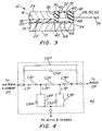
Figure 3 is a view taken along line 3-3 of Figure 2.
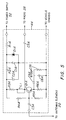
Figure 4 is an electrical schematic of a representative passive
impedance matching network.
Figure 5 is an electrical schematic of a representative active
impedance matching network.
Figure 6 is a view similar to Figure 3 illustrating another
embodiment of the present invention.
Figure 7 is a view similar to Figure 1 illustrating another
embodiment of the present invention.
DETAILED DESCRIPTION OF THE INVENTION
The present invention provides a glass antenna system with
improved reception and a method of producing the antenna system and is
disclosed in combination with an antenna system incorporated into an
automotive windshield. However, it should be appreciated that the
present invention may be used in other transmitting and/or receiving
antenna systems where it is important to match the impedance of the
system components and optimize performance over a wide frequency
band, e.g. cellular phone or television antenna systems.
Figure 1 illustrates an antenna system 10 including a laminated
vehicle windshield 12 formed by outer and inner glass plies 14 and 16,
respectively, which are bonded together by a thermoplastic interlayer 18,
preferably polyvinyl butyral. Plies 14 and 16 may be other transparent
rigid materials, for example acrylic, polycarbonate, or the windshield 12
may include a combination of different transparent, rigid materials.
Windshield 12 further includes at least one antenna element 20. In the
particular antenna configuration illustrated in Figure 1, the antenna
element 20 is a transparent electroconductive coating applied on surface
22 of glass ply 14 in any manner well known in the art, and generally
occupies the central portion of the windshield 12. The coating may be a
single or multilayered metal containing coating, for example as disclosed
in U.S. Patent Nos. 3,655,545 to Gillery et al.; 3,962,488 to Gillery; and
4,898,789 to Finley. It should be appreciated that the antenna element
20 may have a configuration different from that shown in Figure 1. For
example, antenna element 20 may be T-shaped as disclosed in U.S.
Patent No. 5,083,135 or may include multiple elements having various
shapes as disclosed in U.S. Patent No. 5,528,514. The windshield 12
may further include a decorative border (not shown) bonded to the
marginal edge portion of the windshield 12. This border is typically
formed from a ceramic paint applied to surface 24 of inner ply 16.
Although the antenna element 20 discussed above is a transparent
coating, if the antenna element is not positioned in the major vision area
of the windshield 12 or does not obstruct the windshield's main viewing
area, antenna element 20 may be a nontransparent electroconductive
material, for example silver-containing ceramic paint, wires, metal foil,
etc. In addition, the antenna element 20 may include a combination of
coating, wire and/or ceramic antenna elements.
It should be appreciated that the antenna element does not have to
be secured to a major surface of a rigid ply of a transparency. More
specifically, the antenna element may be incorporated into a flexible ply.
For example, and without limiting the present invention, an antenna wire
or electroconductive coating may be positioned on or within an interlayer
18. It is also contemplated that the antenna element may be applied to a
flexible substrate, such as a polyester film (PET), which in turn is
incorporated into the interlayer 18, as disclosed in U.S. Patent No.
5,306,547 to Hood et al.
With continued reference to Figure 1, antenna element 20 in this
particular configuration is basically quadrilateral in shape and preferably
spaced from the peripheral edge of the windshield 12. The exact shape
and position of antenna element 20, as well as any additional antenna
elements depends in part on the design of the vehicle into which the
windshield 12 is installed, the angle of windshield installation, the coating
resistivity, the type of signal to be transmitted or received and the desired
performance of the antenna. These types of design considerations for a
transparent glass antenna are discussed in U.S. Patent Nos. 4,768,037;
4,849,766 and 5,083,135.
Referring to Figures 2 and 3, an antenna feed arrangement 26
provides a connection between the antenna element 20 and an electromagnetic
energy transmitting and/or receiving unit 28 (shown only in
Figure 1) via a feedline, e.g. a coaxial cable 30, which incorporates an
impedance matching network into the antenna system 10, as will be
discussed later in more detail. In a preferred embodiment of the invention,
the antenna feed arrangement 26 includes a connector 32 secured to the
windshield 12, as will be discussed later in more detail. Unit 28 may be a
radio, cellular phone, television, global positioning system or any other
type of system that uses antenna element 20 to transmit and/or receive
signals. Although not required, in the particular antenna arrangement
shown in Figure 1, the connector 32 is positioned along the upper edge
34 of the windshield 12. The connection arrangement between the
connector 32 and antenna element 20 of feed arrangement 26 is
configured such that the connector 32 is not laminated between plies 14
and 16. In this manner, the problem of entrapped air resulting from a
connector being laminated within the windshield 12 is eliminated. More
specifically, a notch area 36 is cut out of the inner ply 16 along the upper
edge 34 of the windshield 12, as shown in Figures 1 to 3. In one
particular embodiment of the connector arrangement, a corresponding
section of the interlayer 18 is removed from the notch area 36.
Connector 32 is adhered and electrically coupled to a portion of the
antenna element 20 that extends into the notch area 36. The notch
area 36 is filled with a sealant material 38 to further secure the connector
32 in place and seal the notch area 36, as will be discussed later in more
detail. Where the antenna and notch area configuration are such that a
portion of antenna element 20 passes through the notch area 36, the
connector 32 is secured directly to antenna element 20. As an
alternative, the antenna feed system 26 may include an extension 40
which extends the antenna element 20 into the notch area 36 and
provides an arrangement whereby the connector 32 may be electrically
coupled to the antenna element 20 through extension 40. Depending on
the antenna design, extension 40 may or may not be an antenna element.
It should be appreciated that when the present disclosure states that the
connector or impedance matching network is electrically coupled to
antenna element 20, the coupling may be directly to antenna element 20
or to element 20 through extension 40 as discussed above. Although not
required, the extension 40 may be made of the same material as antenna
element 20. It is preferred that the antenna element 20 or extension 40
should not extend to the edge 34 of the windshield 12 at notch area 36
but rather terminate at least 1 mm from the edge 34 to ensure that the
electroconductive antenna elements are completely sealed within the
notch area 36 by sealant 38 to inhibit degradation of the antenna element
20 along edge 34.
As discussed earlier, it is important that the impedance of the
antenna component of the antenna system match that of the other
system components in order to optimize the antenna system performance.
In the present invention, this optimization is accomplished by
incorporating an impedance matching network into the antenna system,
and in particular the network is provided in the form of a printed circuit
board that is incorporated into connector 32 of the feed arrangement 26
and secured directly to the windshield 12. The impedance matching
network serves to couple all of the radio frequency energy generated by
the antenna and make it available to the radio. In addition, by
incorporating the impedance matching network into the connector 32 that
is secured to the antenna element 20 of windshield 12, there is negligible
loss in the transfer of signal from the antenna to the impedance matching
network.
Using an impedance matching network provides additional
advantages. Because the output impedance of the antenna is manipulated
by the matching network, there is more flexibility in the design of the
antenna elements of the overall system. More specifically, designing the
antenna to have a desired impedance, e.g. a value that closely matches
that of the radio 28 and coaxial cable 30, would no longer be required
since the impedance matching network will perform the same function.
Furthermore, the impedance matching network will provide better
matching of the impedance over the entire FM frequency band so that
there will be a more efficient power transfer from the antenna element 20
to the radio 28.
In the present invention, the impedance matching network may be
either a passive impedance matching network or an active impedance
matching network. A passive impedance matching network is a circuit
which uses a combination of electrical components, e.g. capacitors and
inductors, to divide the FM signal into several wavelength bands and to
change the impedance of each band to be closer to that of the
radio 28
and
coaxial cable 30. Although not limiting in the present invention,
Figure 4 illustrates a representative passive
impedance matching network
42 which uses inductors L1P through L5P and capacitors C1P through
C5P to form a standard double PI network for the FM signal, wherein each
leg can have inductance and/or capacitance. An additional inductor L6P
and capacitor C6P are used to carry the AM signal around the
network
42. It should be appreciated that since the impedance of the antenna
changes at different frequencies, the passive impedance matching
network can only represent a compromise, although it provides a
significantly better performance than an antenna system without such an
impedance matching network. In addition, the electrical characteristics of
the components of the passive
impedance matching network 42 may vary
based on the vehicle into which similarly designed antennas are installed
because the impedance of the
antenna system 10 is based in part on the
vehicle body design. Furthermore, based on the vehicle and antenna
design, some of the electrical components of the passive
impedance
matching network 42 of the configuration shown in Figure 4 may not be
required. An advantage in using a passive impedance matching network
is that no additional power is required to operate the circuit. Table 1
illustrates an example of a passive
impedance matching network 42 of the
configuration shown in Figure 4. The values of the electrical components
were modeled using a computer program that takes measured antenna
impedance at selected frequencies and uses an interactive process that
varies the values of the components to achieve a desired match.
| L1P 0 H | C1P 33 pF |
| L2P |
| 62 nH | C2P 27 pF |
| L3P 0 H | C3P 10000 pF |
| L4P 0.1 H | C4P 0 F |
| L5P 0 H | C5P | 62 pF |
| L6P 1000 nH | C6P 0 F |
H = Henry
F = Farad |
It should be appreciated by those skilled in the art that the value selected
for LAP represents that this component would not be included in this
particular embodiment of the network.
An active impedance matching network is a circuit that
incorporates an amplifier with a relatively high input impedance and a
controlled output impedance. The output impedance is matched to a
desired value, e.g. the impedance of the
radio 28, to optimize the signal
transfer to the
radio 28. One major difference between a passive and an
active impedance matching network is that the latter requires additional
power to produce the required output impedance. It is anticipated that
the power required for an active matching network is about 2mA from the
12 volt car power. In addition, rather than dividing the FM frequency
band into several smaller frequency bands as discussed above with
respect to the passive impedance matching network, the active
impedance matching network transforms the impedance of the antenna
component to a desired value, regardless of the radio frequency.
Although not limiting in the present invention, Figure 5 illustrates a
representative active
impedance matching network 44. The basic circuit
of
active matching network 44 is a standard common emitter amplifier
using a low noise and a low cost RF transistor Q1A. The signal from the
antenna element 20 is coupled to capacitor C3A to ensure that the bias of
the transistor is not effected by any DC leakage to the electroconductive
coating forming
antenna element 20. The transistor bias is generated by
base resistors R4A and R5A and emitter resistor R6A. The frequency
response and gain are primarily determined by the capacitor C4A and
resistor R7A. To increase the gain of the network at FM frequencies, the
value of R7A is reduced and conversely, to reduce the gain of the network
at FM frequencies, the value of R7A is increased. For a further increase in
FM gain, capacitor C6A in this particular embodiment of the active
network may be installed with values in the range of 10 to 220
picofarads. To increase the gain at AM frequencies, the value of C4A is
increased. The network output is capacitively coupled to the
radio 28
through capacitor C5A so that if the
radio 28 is not capacitively coupled,
it will short out the output. This also allows supplying the power required
for the active
impedance matching network 42 through the
cable 30.
Power to matching
network 42 is provided through resistor R1A and zener
diode D1A to protect against high peak voltages from the vehicle electrical
system. Capacitor C1A provides noise filtering. Resistor R2A and
capacitor C2A provide isolation at radio frequencies and resistor R3A is a
transistor load. Inductor L1 may be used to provide additional gain. One
advantage of using an active impedance matching network is that no
change in components is required for different windshield antenna and/or
vehicle designs because the output impedance is less sensitive to the
antenna and vehicle design. The active impedance matching network will
provide a predetermined output impedance over a wide variation in
antenna component impedance. Therefore, there is more flexibility to the
overall antenna system design. In addition, the active matching network
may be used to improve the AM performance because of amplification of
the signal, and further should provide better overall performance than the
passive matching network, especially for antennas that have a wide
impedance variation. Table 2 illustrates an example of an active
impedance matching network 44 of the configuration shown in Figure 5.
| R1A 1000 Ω | C1A 0.1 uF |
| R2A 2000 Ω | C2A 1000 pF |
| R3A 330 Ω | C3A 0.01 uF |
| R4A 10000 Ω | C4A 4700 pF |
| R5A 7500 Ω | C5A 0.1 F |
| R6A 1000 Ω | C6A 10-220 pF |
| R7A 39 Ω | Q1A NE85633 |
| L1A not used | D1A 10 V |
Ω = Ohms
F = Farad
V = Volts |
It should be appreciated that impedance matching networks 42 and
44 are representative networks that may be used and passive and active
impedance matching networks having different types and number of
components may also be used to match the transform the impedance of
the antenna element 20 in a manner as discussed above.
It is anticipated that either type of matching network may be
constructed on a printed circuit board with an area of about 0.5 square
inches (3.23 sq. cm) and will require a connection to the antenna, a
connection to the coaxial cable 30 and a ground connection, typically to
the vehicle chassis. The active impedance matching network further
requires a power connection which may come from a separate power
connection or through the coaxial cable 30.
In the present invention, the impedance matching network is
incorporated into the connector 32 for the windshield 12. To this end, in
one particular embodiment of the invention, the matching network
circuitry is formed on a circuit board 46 which further includes an output
lead 48 that connects to the coaxial cable 30 and a ground lead 50 that is
grounded to the vehicle body. The active impedance matching network
further includes a lead 52 that connects the network to a power source
54, which preferably is the vehicle battery. Ground lead 50 will operate
as a ground for the power source. Although not limiting in the present
invention, leads 48, 50 and 52 may be wires, e.g. 20 gauge insulated
copper wire, and the ends of wires may include additional connectors to
connect the circuit board 46 to the proper input or output device.
Although not limiting in the present invention, each wire may include a
JASO pin 56 as illustrated in Figure 2, or some other well known type of
end connector. As an alternative, the ends of the leads may be
incorporated into a wiring harness (not shown) to provide for a single
connection of the connector 32 to the antenna system 10. To electrically
couple the connector 32 to the antenna element 20 or extension 40, it is
preferred that the circuit board 46 be positioned such that at least a
portion of the board 46 overlays a portion of antenna element 20 or
extension 40. In one particular embodiment of the invention, the circuit
board 46 is a double sided board with a first surface 58 with a metallic
coating on at least a portion of surface 58 and the printed circuit on its
opposing surface 60. Although not limiting in the present invention, it is
preferred that metallic coating on surface 58 be a solder, e.g. a tin and
lead solder. The electrical components of the matching network on board
46 are positioned within area 62, as indicated in Figure 2. The board 46
is secured within the notch 36 by an adhesive 64 applied along the
surface 58. The adhesive 64 may be electrically conductive to provide a
direct electrical connection between connector 32 and antenna element
20 or extension 40 or it may be electrically nonconductive so that the
electrical connection is capacitive. The adhesive 64 may be applied to the
surface 58 in any convenient manner, e.g. it may be sprayed on or be
applied as a double sided tape. In one particular embodiment of the
invention, the adhesive 64 was 0.002 inch (0.05 mm) thick CD9082
electrically conductive, double sided tape available from Specialty Tapes,
Racine, Wisconsin. In instances where there is a direct electrical
connection between connector 32 and antenna element 20 or extension
40, it may be desirable to have the surface area of the circuit board 46
large enough so that in the event a conductive adhesive 64 fails
electrically, the connector 32 may still maintain a capacitive connection to
antenna element 20 or extension 40 that permits the continued operation
of the antenna system. The surface area of the circuit board 46 of the
connector 32 required for capacitive connection is based in part on the
spacing between the surface 58 and the antenna element 20, i.e. the
adhesive 64 thickness, and the type of materials used for the adhesive.
Electrical connection between opposing surfaces 58 and 60 of board 46
may be made in any convenient manner, for example via an opening 66
which extends through the board 46 and electrically interconnects the
opposing surfaces. If desired colorants may be added to the adhesive 64
to hide the connector 32 when viewed through the outer surface of the
windshield 12.
Although in the particular embodiment of the invention illustrated in
Figure 2, connector 32 is positioned such that the impedance matching
network is electrically coupled to the antenna element 20 by overlaying
and being secured to extension 40, it is anticipated that connector 32
may be positioned such that a portion of the connector 32 overlays and/or
is secured directly to surface 22 of glass ply 14. It is further
contemplated that the connector 32 may be positioned entirely on surface
22 of ply 14 and an additional lead element (not shown) electrically
couple the impedance matching network to antenna element 20 or
extension 40.
As discussed earlier, the connector 32 is positioned within the
notch 36 along edge 34 of the windshield 12. The notch 36 must be
large enough to accommodate connector 32 as well as provide sufficient
spacing between edge 68 of the connector 32 and edge 34 of the
windshield 12 to ensure that the sealant 38 completely covers and seals
connector 32 within the notch area 36 and provides a continuous
moisture barrier along the windshield edge 34 and notch edge 70. The
spacing between the connector edge 68 and windshield edge 34 should
be at least 1 millimeter and preferably at least 3 millimeters.
It is preferred to minimize the thickness of the board 46 and the
size of the circuit components. This is particularly important where the
connector 32 will positioned within a notch area 36 of the windshield 12
as discussed herein. More specifically, the connector 32 should have a
total thickness of no greater than about 0.12 inches (3.05 mm) which is
the depth of the notch area 36. In one embodiment of the invention, it is
expected that the board 46 will be approximately 0.037 inches (0.75 mm)
thick and include an adhesive 64 that is about 0.002 inches (0.051 mm)
thick and further that the maximum height of the network components be
about 0.063 inches (1.6 mm) for a total connector thickness of
approximately 0.096 inches (2.44 mm).
The notch area 36 is filled with a nonconductive sealant 38 to
protect and further secure the connector 32 in place, to seal the portion of
the antenna element 20 within notch area 36, and to seal the exposed
edge 70 of the notch area 36 by forming a moisture barrier. In addition, it
is preferred that the surface 72 of the sealant 38 along with surface 24 of
the inner glass ply 16 to provide a smooth, hard uninterrupted surface
along the surface 24 of inner ply 16 of the windshield 12 so as not to
interfere with the windshield adhesive application and mounting system.
Although not limiting in the present invention, the sealant 38 is preferably
a room temperature curable material that may be injected into the notch
36 and provide a hard surface when cured, preferably a Shore A Hardness
of at least about 85. Furthermore, the sealant should not adversely effect
the materials forming the antenna element 20 or extension 40 in a manner
that will electrically isolate the connector 32 from the antenna nor should
it adversely affect the circuitry of the impedance matching network of
connector 32. If desired, the network may be encased in a protective
material prior to installation.
In a particular embodiment of the invention, the notch area 36 may
be filled with Scotch-Weld DP-110 epoxy, available from 3M Company,
St. Paul, Minnesota, which is a nonconductive room temperature curable,
two-part epoxy. This particular sealant may be modified by adding silane,
e.g. Dow Corning® Z-6040 silane available from Dow Corning, Midland,
Michigan, to the epoxy resin component in an amount equal to approximately
0.2 to 8 wt.% of the resin, and preferably 0.5 to 2 wt.%, to
improve bonding of the sealant to the glass. In addition, carbon black, for
example Arospere™ 11V carbon black available from J.M. Huber
Corporation, Borger, Texas, may be added to "hide" the filled notch by
providing a black appearance consistent with a black ceramic border (not
shown) which is typically applied about the marginal edge portion of an
automotive vehicle windshield 12. Carbon black may also be added to the
accelerator component of the epoxy in an amount equal to approximately
1 to 1.5 wt.% of the accelerator. As applied, this sealant will set up in
about 15 minutes so that it may be handled more easily. It should be
appreciated that heating this particular epoxy sealant prior to and/or after
application will reduce its cure time. When completely cured, it is
expected that the epoxy will have a Shore A hardness of about 88. As an
alternative to the sealant discussed above, Plastilok® 421 epoxy, which is
a two-part flexible epoxy available from BF Goodrich, Adhesive Systems
Division, Akron, Ohio, or W041696 T1 Black, a two-part structural
adhesive available from Advanced Polymer Concepts, Germantown,
Wisconsin, may also be used to seal notch 36.
Although in the particular embodiments of the invention discussed
above, the impedance matching network was mounted on a circuit board,
the network components may be mounted on other types of substrates,
such as but not limited to, a plastic substrate. In addition, the impedance
matching network may be incorporated into an integrated circuit that is
positioned and secured to the windshield 12 so that it is electrically
coupled to antenna element 20 in a manner as discussed earlier with
respect to the circuit board. It is further contemplated that the substrate
may be eliminated and the impedance matching network components be
mounted directly in the glass surface 22 and/or antenna element 20 or
extension 40. The impedance matching network in such a form may be
positioned within the notch area 36 and sealed in the manner discussed
earlier.
It is anticipated that connector 32 with an impedance matching
network as discussed above may be secured to the windshield 12 without
using adhesive 64. More specifically, the connector may be soldered
directly to glass surface 22 of outer ply 14 or to antenna element 20 or
extension 40. It is further contemplated that the impedance matching
network may secured to windshield 12 by mounting and electrically
interconnecting the impedance matching network to a metal strip or
connector clip of a type well known in the art and securing the strip or
clip to ply 14, antenna element 20 or extension 40 in any convenient
manner, e.g. solder or adhesive tape.
In fabricating the windshield 12 described above, the transparent
electroconductive coating is applied to surface 24 of glass ply 14 in any
manner well known in the art, using a mask to provide the desired
antenna pattern. As an alternative, the entire surface 22 of ply 14 may
be coated and thereafter selected portions of the coating removed to
provide the desired antenna pattern. As discussed earlier, it is preferred
that the edge of the coating be spaced from the edge of the glass sheet
14 to ensure that the coating is sealed within the windshield 12. It is
further desirable to space the coating from the edge of sheet 14 a
distance sufficient to avoid any capacitively coupling between the antenna
coating and the metal frame of the vehicle which could adversely effect
the performance of the antenna system. Although not limiting in the
present invention, in one embodiment, the coating was spaced a minimum
of about 13 mm from the edge of sheet 14. After coating, ply 14 is
combined with ply 16, which includes the cut-out area corresponding to
notch area 36, and the two plies are shaped simultaneously using
techniques well known in the art, for example gravity sag bending. If
desired, plies 14 and 16 may be shaped individually and/or prior to
applying the antenna element 20. After shaping, the interlayer 18 is
inserted between plies 14 and 16, with a cut out section in the interlayer
18 corresponding to the notch area 36. The entire assembly is then
de-aired and laminated using techniques well known in the art to form a
unitary structure. After lamination, the notch area 36 is wiped clean and
connector 32 is secured to extension 40 by adhesive 64 within notch
area 36. Although not limiting in the present invention, in one embodiment,
the connector 32 was spaced about 15 mm from the edge 34 of
sheet 14 The ends of leads 48 and 50 (and 52 for an active matching
network) are then removed from the notch 36 and the notch is subsequently
filled with a nonconductive sealant 38.
Although the invention as discussed above included only one
electrical connection to the antenna element 20, it should be appreciated
that multiple connections to the antenna element 20 of the type disclosed
herein may be made along one or several edges of the windshield 12 in a
manner similar to that disclosed herein.
Referring to Figure 6, it is anticipated that the impedance matching
networks disclosed herein may be used to form a capacitive connection to
antenna element 20 within a laminate with a connector being secured to
an outer major surface of the laminate, e.g. a connector 32 secured to
surface 24 of inner ply 16 of windshield 12. A problem with using a
capacitive type connection in this type of arrangement is the required size
of the connector. The effectiveness of the capacitive coupling depends
on the size of the connector and the frequency of the signal. Relatively
high frequencies, such as FM radio signals, require less area than lower
frequencies, such as AM radio signals. It is anticipated that for the lower
frequency AM signals, a connector positioned along surface 24 of ply 16
must overlay approximately 20 square inches (129 square centimeters) of
the antenna coating 20 to provide a connection equivalent to a direct
electrical connection, based on the electrical characteristics of 0.090 inch
(2.23 mm) thick glass ply 16 and 0.030 inch (0.76 mm) thick polyvinyl
butyral interlayer 18 and an electroconductive coating 20 of approximately
3 to 4 ohms per square. It is believed that the size of the
connector 32 may be reduced to approximately 1 to 5 square inches
(6.54 to 32.26 sq./cm) and the matching network incorporated into the
connector 32 be used to match the impedance and boost the AM signal.
The connector as disclosed herein may also be used in combination
with antenna systems wherein the antenna elements are not laminated
within a transparency. More specifically, referring to Figure 7,
transparency 112 of system 110 includes antenna elements 120 secured
to surface 124 of the transparency. Transparency 112 is a glass or
plastic ply that may be the back or side window of a vehicle. Elements
120 may be a coating, wires and/or an electroconductive ceramic paint,
as is well know in the art. Connector 132, which is similar in
construction to connector 32 discussed earlier, may be secured to surface
124 such that it overlays a portion of the element 120. The connection
between antenna elements 120 and connector 132 may be a direct or
capacitive connection, depending on the type of adhesive used. It is
anticipated that the connector 132 may require a protective coating to
protect the network components along the connector's printed circuit
board. It should be appreciated that if the transparency 112 further
includes a heating system (not shown) of a type well known in the art,
and power for the heating system is supplied through the connector 132,
the impedance matching network circuitry will require additional
components to isolate the AC signal from the antenna from the DC
current providing power to the heating system
Based on the disclosure herein, it is anticipated that a transparent
antenna system may be manufactured in a manner such that the antenna
element is incorporated into a flexible ply and the connector is secured to
the flexible ply such that its impedance matching network is electrically
coupled to the antenna element. If desired, this flexible antenna system
may then be combined with other plies. For example, the flexible antenna
may be secured to one or more rigid plies, such as glass or plastic, to
form a laminate, or it may be positioned between two spaced apart glass
sheets in an architectural glazing unit.
The invention described and illustrated represent a description of
illustrative preferred embodiments thereof. It is understood that various
changes may be made without departing from gist of the invention
defined by the claims that follow.