EP0848835B1 - Technique for fabrication of a poled electro-optic fiber segment - Google Patents
Technique for fabrication of a poled electro-optic fiber segment Download PDFInfo
- Publication number
- EP0848835B1 EP0848835B1 EP96933748A EP96933748A EP0848835B1 EP 0848835 B1 EP0848835 B1 EP 0848835B1 EP 96933748 A EP96933748 A EP 96933748A EP 96933748 A EP96933748 A EP 96933748A EP 0848835 B1 EP0848835 B1 EP 0848835B1
- Authority
- EP
- European Patent Office
- Prior art keywords
- fiber
- fiber segment
- poling
- segment
- substrate
- Prior art date
- Legal status (The legal status is an assumption and is not a legal conclusion. Google has not performed a legal analysis and makes no representation as to the accuracy of the status listed.)
- Expired - Lifetime
Links
- 239000000835 fiber Substances 0.000 title claims description 111
- 238000000034 method Methods 0.000 title claims description 24
- 238000004519 manufacturing process Methods 0.000 title claims description 17
- 230000005684 electric field Effects 0.000 claims description 20
- 239000004642 Polyimide Substances 0.000 claims description 11
- 229920001721 polyimide Polymers 0.000 claims description 11
- 239000000758 substrate Substances 0.000 claims description 11
- 229910052751 metal Inorganic materials 0.000 claims description 5
- 239000002184 metal Substances 0.000 claims description 5
- 238000002955 isolation Methods 0.000 claims description 4
- 239000003989 dielectric material Substances 0.000 claims description 3
- 238000005498 polishing Methods 0.000 claims description 3
- 238000004026 adhesive bonding Methods 0.000 claims description 2
- 238000000151 deposition Methods 0.000 claims 4
- 230000001939 inductive effect Effects 0.000 claims 2
- 238000005530 etching Methods 0.000 claims 1
- 239000003365 glass fiber Substances 0.000 claims 1
- 230000003287 optical effect Effects 0.000 description 17
- VYPSYNLAJGMNEJ-UHFFFAOYSA-N Silicium dioxide Chemical compound O=[Si]=O VYPSYNLAJGMNEJ-UHFFFAOYSA-N 0.000 description 7
- 239000013307 optical fiber Substances 0.000 description 7
- 230000008569 process Effects 0.000 description 7
- 238000005253 cladding Methods 0.000 description 6
- 230000008878 coupling Effects 0.000 description 6
- 238000010168 coupling process Methods 0.000 description 6
- 238000005859 coupling reaction Methods 0.000 description 6
- 238000004806 packaging method and process Methods 0.000 description 6
- 230000005540 biological transmission Effects 0.000 description 5
- 230000000694 effects Effects 0.000 description 5
- 238000004891 communication Methods 0.000 description 4
- 239000000463 material Substances 0.000 description 4
- 238000005259 measurement Methods 0.000 description 4
- 238000009281 ultraviolet germicidal irradiation Methods 0.000 description 4
- 230000015556 catabolic process Effects 0.000 description 3
- 230000010363 phase shift Effects 0.000 description 3
- 238000012545 processing Methods 0.000 description 3
- 238000012552 review Methods 0.000 description 3
- 229910003327 LiNbO3 Inorganic materials 0.000 description 2
- QAOWNCQODCNURD-UHFFFAOYSA-N Sulfuric acid Chemical compound OS(O)(=O)=O QAOWNCQODCNURD-UHFFFAOYSA-N 0.000 description 2
- 239000002131 composite material Substances 0.000 description 2
- 230000009977 dual effect Effects 0.000 description 2
- 238000005516 engineering process Methods 0.000 description 2
- 238000002474 experimental method Methods 0.000 description 2
- 239000005350 fused silica glass Substances 0.000 description 2
- 230000003993 interaction Effects 0.000 description 2
- 230000000737 periodic effect Effects 0.000 description 2
- 230000004044 response Effects 0.000 description 2
- 239000000377 silicon dioxide Substances 0.000 description 2
- 206010034972 Photosensitivity reaction Diseases 0.000 description 1
- 230000005697 Pockels effect Effects 0.000 description 1
- 239000000853 adhesive Substances 0.000 description 1
- 230000001070 adhesive effect Effects 0.000 description 1
- WYTGDNHDOZPMIW-RCBQFDQVSA-N alstonine Natural products C1=CC2=C3C=CC=CC3=NC2=C2N1C[C@H]1[C@H](C)OC=C(C(=O)OC)[C@H]1C2 WYTGDNHDOZPMIW-RCBQFDQVSA-N 0.000 description 1
- 229910021486 amorphous silicon dioxide Inorganic materials 0.000 description 1
- 238000013459 approach Methods 0.000 description 1
- 230000008901 benefit Effects 0.000 description 1
- 239000007767 bonding agent Substances 0.000 description 1
- 239000011248 coating agent Substances 0.000 description 1
- 238000000576 coating method Methods 0.000 description 1
- 229910052681 coesite Inorganic materials 0.000 description 1
- 230000001427 coherent effect Effects 0.000 description 1
- 229910052906 cristobalite Inorganic materials 0.000 description 1
- 238000013461 design Methods 0.000 description 1
- 239000002019 doping agent Substances 0.000 description 1
- 238000012681 fiber drawing Methods 0.000 description 1
- 239000011521 glass Substances 0.000 description 1
- 239000003292 glue Substances 0.000 description 1
- 230000006872 improvement Effects 0.000 description 1
- 238000003780 insertion Methods 0.000 description 1
- 230000037431 insertion Effects 0.000 description 1
- 230000010354 integration Effects 0.000 description 1
- 230000005693 optoelectronics Effects 0.000 description 1
- 230000036211 photosensitivity Effects 0.000 description 1
- 239000004033 plastic Substances 0.000 description 1
- 230000010287 polarization Effects 0.000 description 1
- 238000010248 power generation Methods 0.000 description 1
- 230000001902 propagating effect Effects 0.000 description 1
- 238000005086 pumping Methods 0.000 description 1
- 229910052761 rare earth metal Inorganic materials 0.000 description 1
- 238000011160 research Methods 0.000 description 1
- 229910052682 stishovite Inorganic materials 0.000 description 1
- 238000012360 testing method Methods 0.000 description 1
- 229910052905 tridymite Inorganic materials 0.000 description 1
Images


Classifications
-
- G—PHYSICS
- G02—OPTICS
- G02F—OPTICAL DEVICES OR ARRANGEMENTS FOR THE CONTROL OF LIGHT BY MODIFICATION OF THE OPTICAL PROPERTIES OF THE MEDIA OF THE ELEMENTS INVOLVED THEREIN; NON-LINEAR OPTICS; FREQUENCY-CHANGING OF LIGHT; OPTICAL LOGIC ELEMENTS; OPTICAL ANALOGUE/DIGITAL CONVERTERS
- G02F1/00—Devices or arrangements for the control of the intensity, colour, phase, polarisation or direction of light arriving from an independent light source, e.g. switching, gating or modulating; Non-linear optics
- G02F1/35—Non-linear optics
- G02F1/355—Non-linear optics characterised by the materials used
- G02F1/3558—Poled materials, e.g. with periodic poling; Fabrication of domain inverted structures, e.g. for quasi-phase-matching [QPM]
-
- G—PHYSICS
- G02—OPTICS
- G02B—OPTICAL ELEMENTS, SYSTEMS OR APPARATUS
- G02B6/00—Light guides; Structural details of arrangements comprising light guides and other optical elements, e.g. couplings
- G02B6/02—Optical fibres with cladding with or without a coating
-
- G—PHYSICS
- G02—OPTICS
- G02B—OPTICAL ELEMENTS, SYSTEMS OR APPARATUS
- G02B6/00—Light guides; Structural details of arrangements comprising light guides and other optical elements, e.g. couplings
- G02B6/24—Coupling light guides
- G02B6/245—Removing protective coverings of light guides before coupling
-
- G—PHYSICS
- G02—OPTICS
- G02B—OPTICAL ELEMENTS, SYSTEMS OR APPARATUS
- G02B6/00—Light guides; Structural details of arrangements comprising light guides and other optical elements, e.g. couplings
- G02B6/02—Optical fibres with cladding with or without a coating
- G02B6/02057—Optical fibres with cladding with or without a coating comprising gratings
- G02B6/02076—Refractive index modulation gratings, e.g. Bragg gratings
-
- G—PHYSICS
- G02—OPTICS
- G02B—OPTICAL ELEMENTS, SYSTEMS OR APPARATUS
- G02B6/00—Light guides; Structural details of arrangements comprising light guides and other optical elements, e.g. couplings
- G02B6/24—Coupling light guides
- G02B6/26—Optical coupling means
- G02B6/28—Optical coupling means having data bus means, i.e. plural waveguides interconnected and providing an inherently bidirectional system by mixing and splitting signals
- G02B6/2804—Optical coupling means having data bus means, i.e. plural waveguides interconnected and providing an inherently bidirectional system by mixing and splitting signals forming multipart couplers without wavelength selective elements, e.g. "T" couplers, star couplers
- G02B6/2821—Optical coupling means having data bus means, i.e. plural waveguides interconnected and providing an inherently bidirectional system by mixing and splitting signals forming multipart couplers without wavelength selective elements, e.g. "T" couplers, star couplers using lateral coupling between contiguous fibres to split or combine optical signals
- G02B6/2843—Optical coupling means having data bus means, i.e. plural waveguides interconnected and providing an inherently bidirectional system by mixing and splitting signals forming multipart couplers without wavelength selective elements, e.g. "T" couplers, star couplers using lateral coupling between contiguous fibres to split or combine optical signals the couplers having polarisation maintaining or holding properties
-
- G—PHYSICS
- G02—OPTICS
- G02F—OPTICAL DEVICES OR ARRANGEMENTS FOR THE CONTROL OF LIGHT BY MODIFICATION OF THE OPTICAL PROPERTIES OF THE MEDIA OF THE ELEMENTS INVOLVED THEREIN; NON-LINEAR OPTICS; FREQUENCY-CHANGING OF LIGHT; OPTICAL LOGIC ELEMENTS; OPTICAL ANALOGUE/DIGITAL CONVERTERS
- G02F1/00—Devices or arrangements for the control of the intensity, colour, phase, polarisation or direction of light arriving from an independent light source, e.g. switching, gating or modulating; Non-linear optics
- G02F1/01—Devices or arrangements for the control of the intensity, colour, phase, polarisation or direction of light arriving from an independent light source, e.g. switching, gating or modulating; Non-linear optics for the control of the intensity, phase, polarisation or colour
- G02F1/061—Devices or arrangements for the control of the intensity, colour, phase, polarisation or direction of light arriving from an independent light source, e.g. switching, gating or modulating; Non-linear optics for the control of the intensity, phase, polarisation or colour based on electro-optical organic material
- G02F1/065—Devices or arrangements for the control of the intensity, colour, phase, polarisation or direction of light arriving from an independent light source, e.g. switching, gating or modulating; Non-linear optics for the control of the intensity, phase, polarisation or colour based on electro-optical organic material in an optical waveguide structure
-
- G—PHYSICS
- G02—OPTICS
- G02F—OPTICAL DEVICES OR ARRANGEMENTS FOR THE CONTROL OF LIGHT BY MODIFICATION OF THE OPTICAL PROPERTIES OF THE MEDIA OF THE ELEMENTS INVOLVED THEREIN; NON-LINEAR OPTICS; FREQUENCY-CHANGING OF LIGHT; OPTICAL LOGIC ELEMENTS; OPTICAL ANALOGUE/DIGITAL CONVERTERS
- G02F1/00—Devices or arrangements for the control of the intensity, colour, phase, polarisation or direction of light arriving from an independent light source, e.g. switching, gating or modulating; Non-linear optics
- G02F1/01—Devices or arrangements for the control of the intensity, colour, phase, polarisation or direction of light arriving from an independent light source, e.g. switching, gating or modulating; Non-linear optics for the control of the intensity, phase, polarisation or colour
- G02F1/21—Devices or arrangements for the control of the intensity, colour, phase, polarisation or direction of light arriving from an independent light source, e.g. switching, gating or modulating; Non-linear optics for the control of the intensity, phase, polarisation or colour by interference
- G02F1/225—Devices or arrangements for the control of the intensity, colour, phase, polarisation or direction of light arriving from an independent light source, e.g. switching, gating or modulating; Non-linear optics for the control of the intensity, phase, polarisation or colour by interference in an optical waveguide structure
Definitions
- This invention relates to a method for the fabrication of electrooptically active fiber segments that can be readily integrated into optical fiber lines, with applications in high-speed modulators, electric field sensors, or optical mixers.
- This invention is related to U. S. Patents 5,239,407, Method and Apparatus for Creating Large Second-Order Nonlinearities in Fused Silica and 5,247,601, Arrangement for Producing Large Second-Order Optical Nonlinearities in a Waveguide Structure including Amorphous SiO 2 .
- Packaging costs associated with opto-mechanical coupling of discrete optical components are a major part of the cost for advanced optoelectronic systems.
- the output of a diode laser must be coupled into a single-mode optical fiber, the fiber must then be coupled to a LiNbO 3 waveguide modulator whose output is again coupled into a fiber.
- Discrete optical components e. g., graded-index lenses or micro-lenses are required at each coupling node to adapt the very different mode profiles and spatial extents of the diode laser and modulator waveguide modes to the fiber mode. Tolerances are fractions of a micrometer to ensure minimal coupling losses and extensive active alignment (optimizing coupling with the laser on) is typically required. Throughput and yield are both limited by the requirement of keeping the system stable while the bonding agents cure. If a modulator could be produced that was integrated into the fiber, the manufacturing and packaging costs associated with these high-speed fiber communications systems would be substantially reduced.
- Electric field sensors are another potentially attractive application of electrooptically active fibers.
- the electric power industry has a need for remote sensors to monitor high voltage power systems.
- Integrating electrooptically active fiber sensors with Bragg reflector gratings is a very attractive alternative to currently available sensors that will have a major economic impact.
- a third potential area of application of electrooptically active fibers is frequency mixing (i.e., second harmonic and sum frequency generation to reach shorter wavelengths than the starting wavelengths and difference frequency generation to reach longer wavelengths).
- frequency mixing i.e., second harmonic and sum frequency generation to reach shorter wavelengths than the starting wavelengths and difference frequency generation to reach longer wavelengths.
- Applications include high-density optical recording, displays, and spectroscopic sensors.
- These nonlinear mixing processes require both a second-order nonlinearity, the same order nonlinearity that gives rise to the electrooptic effect, as well as a phase matching technique to ensure that the nonlinear mixing stays coherent along the active length of the fiber.
- phase matching is most conveniently achieved by quasi-phase matching in which the nonlinearity is alternately turned on and off each coherence length (i.e., the length over which the phases of the fundamental and second harmonic fields are shifted by ⁇ because of their different velocities). More complex poling patterns may be desirable to tailor the phase matching bandwidth for specific applications.
- the fiber is drawn from a preform with two holes for electrode wires that are to be inserted following the fiber drawing.
- This wire insertion is a difficult manufacturing step, comparable to the difficulty and expense of coupling discrete optical components.
- one wire is inserted from each end of the fiber. This means that the modulation frequency is limited to low values since a high-speed traveling wave geometry is not possible.
- splicing to either end of the fiber is not possible because of the electrodes again requiring discrete optical system alignment for coupling into the fibers, negating much of the advantage of an electrooptically active fiber segment - the fabrication of an all-fiber active device.
- the present invention provides a method of fabricating an electrooptically active fiber segment, and products made therefrom in accordance with the claims which follow.
- a electrooptically active fiber segment is fabricated using a D-shaped or "D" fiber where one side of the cladding has been removed close to the core.
- This flat side of the fiber is glued to a substrate which has been made suitably conductive to form one of the device electrodes.
- the fiber ends extend beyond the substrate for subsequent fiber splicing.
- a thick layer of dielectric is deposited on the substrate, and the fiber/dielectric structure is polished to provide a planar surface and close access to the fiber core on the side of the fiber opposite to the flat portion of the "D.”
- This dielectric layer also provides electrical isolation so that large voltages can be applied across the fiber core in the poling process.
- a second electrode is deposited on top of the polished surface, forming a stripline to allow high-speed rf propagation. Temperature/electric field poling of the composite structure creates a second-order nonlinearity in the fiber enabling modulation of a propagating laser beam by an electromagnetic signal. Alternately, electric fields can be applied along with appropriate UV irradiation to form the nonlinearity, or a combination including temperature programming along with UV irradiation can be used. A second dielectric layer followed by a blanket metal film may be added for additional rf isolation.
- This technology provides: (a) a high-speed rf circuit allowing traveling wave interactions between the rf and optical fields and hence a high speed modulation capability; (b) inexpensive optical packaging by simple splices at both ends of the fiber; and (c) extensibility to simultaneous manufacture of multiple poled fiber, electrooptically active sections.
- a fiber modulator refers to Figure 2.
- the electrooptically active fiber section 31 is spliced to two additional passive fiber sections 32, 33 which are connected to two 3dB 2x1 fiber power splitters 34, 35.
- An additional passive fiber section 36 between the power splitters completes the Mach-Zehnder interferometer.
- the phase shift of the optical signal transmitted through the electrooptically active fiber section is modulated by application of an electric field across the electrodes 37, 38 .
- the transmission through the interferometer is a sinusoidal function of the optical phase difference between the two arms of the interferometer.
- the transmission When the two signals are in phase at the output power splitter, the transmission is maximum; when the two signals are ⁇ out of phase at the output power splitter, the transmission is zero and all of the power is reflected from the interferometer.
- the passive fiber segment 36 is replaced with a second electrooptically active segment with opposite polarity electric fields applied, reducing the required voltage swing by a factor of two.
- the electrooptically active segment could again be incorporated in an all-fiber integrated Mach-Zehnder interferometer, now with the electrodes 37, 38 removed to allow sensing of the local electric field in the region of the electrooptically active fiber segment.
- a Bragg grating 41 could be incorporated in the electrooptically active fiber segment.
- the Bragg grating is a region of refractive index modulation that reflects light of a certain frequency range and transmits light of other frequency ranges.
- the specific frequency of minimum transmission can be modified by changing the overall modal index of the fiber by applying an electric field as shown schematically in the inset to the figure.
- the Bragg grating may be produced by patterned UV-irradiation of the fiber or by any other suitable technique.
- the electrooptically active fiber segment 51 must be poled in a suitable quasi-phase matched configuration as represented by the segmented electrode structure 52 shown in Figure 4.
- Optional Bragg gratings 53, 54 may be placed at either end of the electrooptically active fiber segment to enhance the fields at the fundamental frequencies by forming Fabry-Perot cavities.
- a thin ( ⁇ 1- ⁇ m thick) layer of polyimide (UR3100) was then spun onto a Si wafer and the fiber was affixed to the wafer "D" side down using this polyimide layer as an adhesive.
- the polyimide layer was cured with a dual temperature process at 120°C and 170°C for 5 minutes each. Subsequent to this curing, multiple additional layers of polyimide (UR3140) were spun onto the wafer until the total thickness reached 40 ⁇ m. Each layer of the polyimide was cured with a dual temperature cycle at 120°C and 170°C for 10 minutes each.
- the total polyimide stack was cured at 350°C for 1 hour. Then, the fiber/polyimide structure was mechanically polished down to a thickness of ⁇ 34 ⁇ m. A Cr:Au film (300 ⁇ / 3000 ⁇ ) was deposited on top of the polished surface as the second electrode.
- the resulting structure was poled by electric field/temperature poling processes over a variety of parameters.
- the poled sample was placed in the measurement arm of a Mach-Zehnder interferometer operating at 633 nm.
- the Mach-Zehnder was a free space geometry with appropriate microscope objectives to couple light into and out of the electrooptically active fiber section.
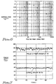
- Figures 5 and 6 show the relationship between the measured electrooptic coefficient r 33 and the poling voltage for a fixed poling temperature of 255°C and a poling time of 10 minutes and of the electrooptic coefficient r 33 vs.
- the phase shift signal is sensitive to the polarization of input laser light.
- the ratio of the signal from TE mode to one from TM mode is ⁇ 2.4:1. This measurement implies that electrooptic coefficient ratio r 33 : r 31 , is ⁇ 2.4:1, roughly consistent with the 3:1 ratio predicted from a simple symmetry model.
- the signal shows a smooth frequency response as shown in figure 7.
- the absence of strong narrow acoustic frequency resonances implies that the piezoelectric response has been damped and demonstrates that the signal is due to the electrooptic effect.
- a scaleable, manufacturing technique for producing a large second-order nonlinearity in an optical fiber is disclosed.
- the resulting electrooptically active fiber segment has an inherent high-speed rf capability with provision for velocity matching of rf and optical fields and is adaptable to periodic poling for quasi-phasematched nonlinear interactions.
- the demonstrated technique is scaleable to volume manufacturing, and is readily packaged with additional fiber components by simple splicing techniques.
- Major areas of application include: high-speed fiber modulators for telecommunications; electric field sensors for power generation and transmission systems; and extended wavelength generation by sum and difference frequency mixing.
Landscapes
- Physics & Mathematics (AREA)
- General Physics & Mathematics (AREA)
- Optics & Photonics (AREA)
- Nonlinear Science (AREA)
- Optical Modulation, Optical Deflection, Nonlinear Optics, Optical Demodulation, Optical Logic Elements (AREA)
- Optical Integrated Circuits (AREA)
Description
Claims (8)
- A method of fabricating an electrooptically active fiber segment (31), comprising the steps of:a) etching or polishing a D-shaped fiber (10) such that the surface of its flat side is close to its core;b) gluing said etched or polished D-shaped fiber to a flat substrate (11) with a conductive surface (12, 37) with ends of said fiber segment extending beyond the substrate;c) placing a portion of said fiber segment between said conductive surface (12,37) and an electrode (15,38);d) inducing or poling a second-order nonlinearity in said fiber segment;
wherein the placing step c) is further characterized by;e) depositing a layer of dielectric material (14) on said substrate, thereby forming a first dielectric layer such that said glass fiber segment is substantially covered by said dielectric layer;f) polishing the fiber/dielectric structure of step e) to provide a planar surface and close access to the fiber core on the side opposite said substrate;g) depositing a first metal layer (15) on said planar surface over said fiber, thereby forming said electrode (15,38). - The method of claim 1, in which a second metal layer (12) is deposited on the flat substrate (11) to provide said conductive surface (12, 37) before step b).
- The method of claim 1 or claim 2, wherein said inducing or poling step d) is performed by at least two of a temperature field means, an electric field means, and a UV light-emitting means.
- The method of any one of claims 1 to 3, wherein the dielectric material (14) is a polyimide.
- The method of any one of claims 1 to 4, further comprising the steps of;h) depositing a second dielectric layer (16) on top of said planar surface; andI) depositing a third metal film (17) on top of said second dielectric layer, thereby adding additional radio frequency (rf) isolation.
- An electrooptically active fiber segment (31) whenever fabricated in accordance with the method of any one of claims 1 to 5.
- An electric field sensor including an electrooptically active fiber segment (31) of claim 6, incorporating a Bragg grating (41).
- A three wave mixer including an electrooptically active fiber segment (51) of claim 6, poled in a quasi-phase matched configuration (52), optionally incorporating a Bragg grating (53,54) at either end of the said fiber segment.
Applications Claiming Priority (3)
| Application Number | Priority Date | Filing Date | Title |
|---|---|---|---|
| US08/525,960 US5617499A (en) | 1995-09-08 | 1995-09-08 | Technique for fabrication of a poled electrooptic fiber segment |
| US525960 | 1995-09-08 | ||
| PCT/US1996/014080 WO1997009644A1 (en) | 1995-09-08 | 1996-09-03 | Technique for fabrication of a poled electro-optic fiber segment |
Publications (3)
| Publication Number | Publication Date |
|---|---|
| EP0848835A1 EP0848835A1 (en) | 1998-06-24 |
| EP0848835A4 EP0848835A4 (en) | 1998-12-02 |
| EP0848835B1 true EP0848835B1 (en) | 2002-07-24 |
Family
ID=24095331
Family Applications (1)
| Application Number | Title | Priority Date | Filing Date |
|---|---|---|---|
| EP96933748A Expired - Lifetime EP0848835B1 (en) | 1995-09-08 | 1996-09-03 | Technique for fabrication of a poled electro-optic fiber segment |
Country Status (6)
| Country | Link |
|---|---|
| US (1) | US5617499A (en) |
| EP (1) | EP0848835B1 (en) |
| JP (1) | JP2002515129A (en) |
| AU (1) | AU7235796A (en) |
| DE (1) | DE69622570T2 (en) |
| WO (1) | WO1997009644A1 (en) |
Families Citing this family (29)
| Publication number | Priority date | Publication date | Assignee | Title |
|---|---|---|---|---|
| AUPM956694A0 (en) * | 1994-11-18 | 1994-12-15 | University Of Sydney, The | Inducing or enhancing electro-optic properties in optically transmissive material |
| US5768462A (en) * | 1996-03-05 | 1998-06-16 | Kvh Industries, Inc. | Grooved optical fiber for use with an electrode and a method for making same |
| DE69711545T2 (en) | 1996-06-04 | 2002-07-25 | The Board Of Trustees Of The Leland Stanford Junior University, Palo Alto | METHOD FOR TREATING OPTICAL FIBERS AND MATERIAL FOR PHASE MODULATORS AND SWITCHES |
| EP0918244A4 (en) | 1996-08-12 | 2001-10-10 | Toyota Motor Co Ltd | DIFFRACTION GRID ELEMENT, LIGHT WAVELENGTH SELECTION USING THE SAME, AND OPTICAL SIGNAL TRANSMISSION SYSTEM |
| US6097867A (en) * | 1996-09-03 | 2000-08-01 | The University Of New Mexico | Technique for fabrication of a poled electro-optic fiber segment |
| JPH1090546A (en) * | 1996-09-17 | 1998-04-10 | Toyota Motor Corp | Manufacturing method of planar waveguide and planar waveguide |
| US6233044B1 (en) | 1997-01-21 | 2001-05-15 | Steven R. J. Brueck | Methods and apparatus for integrating optical and interferometric lithography to produce complex patterns |
| KR100219712B1 (en) * | 1997-02-26 | 1999-09-01 | 윤종용 | Low Loss Active Optical Devices and Manufacturing Method Thereof |
| KR100219714B1 (en) | 1997-02-26 | 1999-09-01 | 윤종용 | Manufacturing method of low loss optical active element |
| JP4097763B2 (en) * | 1997-03-27 | 2008-06-11 | 松下電器産業株式会社 | Secondary nonlinear optical member, method for manufacturing the same, and light modulation element |
| EP0872756A1 (en) * | 1997-04-14 | 1998-10-21 | BRITISH TELECOMMUNICATIONS public limited company | Optical modulator |
| EP1000380A1 (en) | 1997-07-30 | 2000-05-17 | BRITISH TELECOMMUNICATIONS public limited company | Optical waveguide device including an electrical capacitive configuration |
| US5986749A (en) * | 1997-09-19 | 1999-11-16 | Cidra Corporation | Fiber optic sensing system |
| EP1062543A1 (en) * | 1998-02-09 | 2000-12-27 | The University of New Mexico | Tunable bragg gratings and devices employing the same |
| US6385354B1 (en) * | 1998-10-31 | 2002-05-07 | The Board Of Trustees Of The Leland Stanford Junior University | Electrostrictive fiber modulators |
| GB9903882D0 (en) * | 1999-02-19 | 1999-04-14 | Univ Southampton | Optical amplifier |
| JP2000258810A (en) * | 1999-03-08 | 2000-09-22 | Shin Etsu Chem Co Ltd | Secondary optical non-linear glass material and method of manufacturing the same |
| GB9917138D0 (en) * | 1999-07-21 | 1999-09-22 | Univ Southampton | Optical fibres and waveguides |
| AUPQ281199A0 (en) | 1999-09-14 | 1999-10-07 | University Of Sydney, The | Method and apparatus for thermal poling and optical devices |
| EP1143273B1 (en) * | 2000-03-22 | 2011-05-18 | Panasonic Corporation | Fibre optical coupling device |
| US7058245B2 (en) * | 2000-04-04 | 2006-06-06 | Waveguide Solutions, Inc. | Integrated optical circuits |
| KR100392367B1 (en) | 2000-11-06 | 2003-07-22 | 한국전자통신연구원 | Electrode for forming periodically poled optical fibers and fabrication method of periodically poled optical fibers using the same |
| US6587622B2 (en) * | 2001-12-04 | 2003-07-01 | Nortel Networks Limited | Orientation switchable optical fibres |
| RU2247414C2 (en) * | 2002-03-15 | 2005-02-27 | Федеральное государственное унитарное предприятие "Всероссийский научный центр "Государственный оптический институт им. С.И. Вавилова (ФГУП ГОИ) | A single-mode electrooptical fiber and a method of its production |
| KR100420951B1 (en) * | 2002-04-17 | 2004-03-02 | 한국전자통신연구원 | Poled fibers, a method for fabricating a poled fiber, and dispersion compensator |
| KR100518951B1 (en) * | 2003-07-12 | 2005-10-06 | 한국전자통신연구원 | Method for determining efficiency of quasi-phase matching in periodically poled structure of waveguide, periodically poled structure in waveguide and waveguide using the same |
| US9221074B2 (en) * | 2012-10-11 | 2015-12-29 | Octrolix Bv | Stress-tuned planar lightwave circuit and method therefor |
| US10241352B2 (en) | 2017-01-19 | 2019-03-26 | Lionix International Bv | Integrated-optics-based stress-optic phase modulator and method for forming |
| NL2027050B1 (en) | 2020-12-04 | 2022-07-07 | Univ Delft Tech | Fiber-Bragg grating sensor |
Family Cites Families (9)
| Publication number | Priority date | Publication date | Assignee | Title |
|---|---|---|---|---|
| JPS6014222A (en) * | 1983-07-06 | 1985-01-24 | Matsushita Electric Ind Co Ltd | Optical wavelength converting element |
| GB8902533D0 (en) * | 1989-02-04 | 1989-03-22 | Plessey Co Plc | Method for the manufacture of an electro-optic device |
| DE4005557A1 (en) * | 1990-02-22 | 1991-08-29 | Daimler Benz Ag | Fibre=optic intensity modulator - uses light conductor is of D=shaped cross=section with optically active material on its flat surface |
| US5333231A (en) * | 1991-05-02 | 1994-07-26 | Ricoh Company, Ltd. | Wavelength conversion element |
| JP2859464B2 (en) * | 1991-05-15 | 1999-02-17 | 三菱電機株式会社 | Nonlinear optical device |
| US5239407A (en) * | 1991-09-27 | 1993-08-24 | University Of New Mexico | Method and apparatus for creating large second-order nonlinearities in fused silica |
| US5247601A (en) * | 1991-09-27 | 1993-09-21 | Myers Richard A | Arrangement for producing large second-order optical nonlinearities in a waveguide structure including amorphous SiO2 |
| JPH0614222A (en) * | 1992-06-08 | 1994-01-21 | Matsushita Electric Works Ltd | Recording camera device |
| AUPM956694A0 (en) * | 1994-11-18 | 1994-12-15 | University Of Sydney, The | Inducing or enhancing electro-optic properties in optically transmissive material |
-
1995
- 1995-09-08 US US08/525,960 patent/US5617499A/en not_active Expired - Lifetime
-
1996
- 1996-09-03 DE DE69622570T patent/DE69622570T2/en not_active Expired - Lifetime
- 1996-09-03 AU AU72357/96A patent/AU7235796A/en not_active Abandoned
- 1996-09-03 EP EP96933748A patent/EP0848835B1/en not_active Expired - Lifetime
- 1996-09-03 JP JP51132097A patent/JP2002515129A/en active Pending
- 1996-09-03 WO PCT/US1996/014080 patent/WO1997009644A1/en not_active Ceased
Also Published As
| Publication number | Publication date |
|---|---|
| EP0848835A1 (en) | 1998-06-24 |
| JP2002515129A (en) | 2002-05-21 |
| DE69622570T2 (en) | 2003-03-27 |
| AU7235796A (en) | 1997-03-27 |
| DE69622570D1 (en) | 2002-08-29 |
| EP0848835A4 (en) | 1998-12-02 |
| US5617499A (en) | 1997-04-01 |
| WO1997009644A1 (en) | 1997-03-13 |
Similar Documents
| Publication | Publication Date | Title |
|---|---|---|
| US5617499A (en) | Technique for fabrication of a poled electrooptic fiber segment | |
| Long et al. | A poled electrooptic fiber | |
| Tapalian et al. | Thermooptical switches using coated microsphere resonators | |
| US6011881A (en) | Fiber-optic tunable filter | |
| US7283707B1 (en) | Evanescently coupling light between waveguides and whispering-gallery mode optical resonators | |
| US5729641A (en) | Optical device employing edge-coupled waveguide geometry | |
| US6097867A (en) | Technique for fabrication of a poled electro-optic fiber segment | |
| Pan et al. | Waveguide fabrication and high-speed in-line intensity modulation in 4-N, N-4′-dimethylamino-4′-N′-methyl-stilbazolium tosylate | |
| US5076658A (en) | Non-linear optical polymeric fiber waveguides | |
| Takagi et al. | Design and fabrication of broad-band silica-based optical waveguide couplers with asymmetric structure | |
| Long et al. | Large-signal phase retardation with a poled electrooptic fiber | |
| Bai et al. | An in-fiber coupler for whispering-gallery-mode excitation in a microsphere resonator | |
| JP4734053B2 (en) | Mounting deviation compensation method for optical waveguide components | |
| JP3573180B2 (en) | Polling method for Mach-Zehnder interferometer arm | |
| AU757486B2 (en) | Electrostrictive fiber modulators | |
| CN113204149A (en) | Optical fiber integrated optical switch, manufacturing method and optical switching method | |
| Zhu et al. | Highly sensitive balloon-like temperature fiber sensor based on a seven-core fiber | |
| US20030039447A1 (en) | Strip-loaded optical waveguide | |
| Long et al. | Electro-optic effect and second-order optical nonlinearity in poled silica fibers | |
| JP3418391B2 (en) | Method for manufacturing waveguide type optical device | |
| KR100293317B1 (en) | Electro-optic polymer optical waveguide polarization-independent light modulator and its manufacturing method | |
| Wu et al. | High-Q Thin-film Lithium Niobate Asymmetric Microring Resonator with Different Etching Depths and a Multimode Interferometer Coupler | |
| JPH04371913A (en) | Optical modulator and optical switch | |
| Li et al. | Research on Continuously Tunable Optical Delay Line based on Cascaded Micro-ring Resonators | |
| Zheng et al. | Optimal design of a high-speed polymer Mach-Zehnder interferometer electro-optic switch over 260 GHz |
Legal Events
| Date | Code | Title | Description |
|---|---|---|---|
| PUAI | Public reference made under article 153(3) epc to a published international application that has entered the european phase |
Free format text: ORIGINAL CODE: 0009012 |
|
| 17P | Request for examination filed |
Effective date: 19980328 |
|
| AK | Designated contracting states |
Kind code of ref document: A1 Designated state(s): DE FR |
|
| A4 | Supplementary search report drawn up and despatched |
Effective date: 19981020 |
|
| AK | Designated contracting states |
Kind code of ref document: A4 Designated state(s): DE FR |
|
| 17Q | First examination report despatched |
Effective date: 19991223 |
|
| RIN1 | Information on inventor provided before grant (corrected) |
Inventor name: JAIN, DR. RAVINDER K. Inventor name: LONG, XIANG-CUN Inventor name: BRUECK, STEVEN, R., J. |
|
| GRAG | Despatch of communication of intention to grant |
Free format text: ORIGINAL CODE: EPIDOS AGRA |
|
| RIC1 | Information provided on ipc code assigned before grant |
Free format text: 7G 02F 1/35 A, 7G 02B 6/12 B, 7G 02B 6/17 B |
|
| GRAG | Despatch of communication of intention to grant |
Free format text: ORIGINAL CODE: EPIDOS AGRA |
|
| GRAH | Despatch of communication of intention to grant a patent |
Free format text: ORIGINAL CODE: EPIDOS IGRA |
|
| GRAH | Despatch of communication of intention to grant a patent |
Free format text: ORIGINAL CODE: EPIDOS IGRA |
|
| GRAA | (expected) grant |
Free format text: ORIGINAL CODE: 0009210 |
|
| AK | Designated contracting states |
Kind code of ref document: B1 Designated state(s): DE FR |
|
| REF | Corresponds to: |
Ref document number: 69622570 Country of ref document: DE Date of ref document: 20020829 |
|
| ET | Fr: translation filed | ||
| PLBE | No opposition filed within time limit |
Free format text: ORIGINAL CODE: 0009261 |
|
| STAA | Information on the status of an ep patent application or granted ep patent |
Free format text: STATUS: NO OPPOSITION FILED WITHIN TIME LIMIT |
|
| 26N | No opposition filed |
Effective date: 20030425 |
|
| PGFP | Annual fee paid to national office [announced via postgrant information from national office to epo] |
Ref country code: DE Payment date: 20100930 Year of fee payment: 15 |
|
| PGFP | Annual fee paid to national office [announced via postgrant information from national office to epo] |
Ref country code: FR Payment date: 20110901 Year of fee payment: 16 |
|
| REG | Reference to a national code |
Ref country code: FR Ref legal event code: ST Effective date: 20130531 |
|
| PG25 | Lapsed in a contracting state [announced via postgrant information from national office to epo] |
Ref country code: DE Free format text: LAPSE BECAUSE OF NON-PAYMENT OF DUE FEES Effective date: 20130403 |
|
| REG | Reference to a national code |
Ref country code: DE Ref legal event code: R119 Ref document number: 69622570 Country of ref document: DE Effective date: 20130403 |
|
| PG25 | Lapsed in a contracting state [announced via postgrant information from national office to epo] |
Ref country code: FR Free format text: LAPSE BECAUSE OF NON-PAYMENT OF DUE FEES Effective date: 20121001 |