EP0848499A2 - Circuit arrangement for a memory cell in a D/A converter - Google Patents
Circuit arrangement for a memory cell in a D/A converter Download PDFInfo
- Publication number
- EP0848499A2 EP0848499A2 EP97203786A EP97203786A EP0848499A2 EP 0848499 A2 EP0848499 A2 EP 0848499A2 EP 97203786 A EP97203786 A EP 97203786A EP 97203786 A EP97203786 A EP 97203786A EP 0848499 A2 EP0848499 A2 EP 0848499A2
- Authority
- EP
- European Patent Office
- Prior art keywords
- transistor
- transistors
- current
- base
- voltage
- Prior art date
- Legal status (The legal status is an assumption and is not a legal conclusion. Google has not performed a legal analysis and makes no representation as to the accuracy of the status listed.)
- Granted
Links
Images


Classifications
-
- H—ELECTRICITY
- H03—ELECTRONIC CIRCUITRY
- H03K—PULSE TECHNIQUE
- H03K3/00—Circuits for generating electric pulses; Monostable, bistable or multistable circuits
- H03K3/02—Generators characterised by the type of circuit or by the means used for producing pulses
- H03K3/26—Generators characterised by the type of circuit or by the means used for producing pulses by the use, as active elements, of bipolar transistors with internal or external positive feedback
- H03K3/28—Generators characterised by the type of circuit or by the means used for producing pulses by the use, as active elements, of bipolar transistors with internal or external positive feedback using means other than a transformer for feedback
- H03K3/281—Generators characterised by the type of circuit or by the means used for producing pulses by the use, as active elements, of bipolar transistors with internal or external positive feedback using means other than a transformer for feedback using at least two transistors so coupled that the input of one is derived from the output of another, e.g. multivibrator
- H03K3/286—Generators characterised by the type of circuit or by the means used for producing pulses by the use, as active elements, of bipolar transistors with internal or external positive feedback using means other than a transformer for feedback using at least two transistors so coupled that the input of one is derived from the output of another, e.g. multivibrator bistable
- H03K3/288—Generators characterised by the type of circuit or by the means used for producing pulses by the use, as active elements, of bipolar transistors with internal or external positive feedback using means other than a transformer for feedback using at least two transistors so coupled that the input of one is derived from the output of another, e.g. multivibrator bistable using additional transistors in the input circuit
- H03K3/2885—Generators characterised by the type of circuit or by the means used for producing pulses by the use, as active elements, of bipolar transistors with internal or external positive feedback using means other than a transformer for feedback using at least two transistors so coupled that the input of one is derived from the output of another, e.g. multivibrator bistable using additional transistors in the input circuit the input circuit having a differential configuration
-
- H—ELECTRICITY
- H03—ELECTRONIC CIRCUITRY
- H03K—PULSE TECHNIQUE
- H03K3/00—Circuits for generating electric pulses; Monostable, bistable or multistable circuits
- H03K3/02—Generators characterised by the type of circuit or by the means used for producing pulses
- H03K3/26—Generators characterised by the type of circuit or by the means used for producing pulses by the use, as active elements, of bipolar transistors with internal or external positive feedback
- H03K3/28—Generators characterised by the type of circuit or by the means used for producing pulses by the use, as active elements, of bipolar transistors with internal or external positive feedback using means other than a transformer for feedback
- H03K3/281—Generators characterised by the type of circuit or by the means used for producing pulses by the use, as active elements, of bipolar transistors with internal or external positive feedback using means other than a transformer for feedback using at least two transistors so coupled that the input of one is derived from the output of another, e.g. multivibrator
- H03K3/286—Generators characterised by the type of circuit or by the means used for producing pulses by the use, as active elements, of bipolar transistors with internal or external positive feedback using means other than a transformer for feedback using at least two transistors so coupled that the input of one is derived from the output of another, e.g. multivibrator bistable
- H03K3/288—Generators characterised by the type of circuit or by the means used for producing pulses by the use, as active elements, of bipolar transistors with internal or external positive feedback using means other than a transformer for feedback using at least two transistors so coupled that the input of one is derived from the output of another, e.g. multivibrator bistable using additional transistors in the input circuit
-
- H—ELECTRICITY
- H03—ELECTRONIC CIRCUITRY
- H03M—CODING; DECODING; CODE CONVERSION IN GENERAL
- H03M1/00—Analogue/digital conversion; Digital/analogue conversion
- H03M1/66—Digital/analogue converters
- H03M1/74—Simultaneous conversion
- H03M1/742—Simultaneous conversion using current sources as quantisation value generators
Definitions
- the invention relates to a circuit arrangement for a memory cell of a D / A converter and in particular on a memory cell in which an analog Current is switched by a stored digital signal.
- a very common type of D / A converter has a number of stages, to which currents with current values are supplied by current generators, and depending on a binary value stored in the stage, this becomes supplied current forwarded to an output or derived or one forwarded to another output.
- An example of such a D / A converter is in 1 and comprises a number of stages L1, L2 to Ln and a number Current generators CG1, CG2 to CGn.
- Each power generator includes the Series connection of a resistor and a transistor, one end of the Resistor with a line 10 for a reference voltage, i.e. generally with Ground, and the bases of all transistors with a line 11 for an auxiliary voltage are connected.
- the resistors are dimensioned so that in the collector of Transistor of a current generator is a current with twice the value as in that previous current generator flows. These currents become a current input 12 an associated stage L1, L2 to Ln supplied, which depends on this current outputs a digital value stored therein at a current output 20, where all current outputs are connected to each other and thus a total current Is deliver.
- the binary values stored in the individual stages are previously supplied via a data input 16 and by a signal on a control line 14 enrolled in the levels.
- FIG. 2 shows a circuit arrangement for a memory cell of a D / A converter corresponding to one of the stages L1, L2 etc. in Fig. 1, which in conventional analog technology is built.
- the one current input 12 Analog current is fed to the emitters of two transistors Q11 and Q12 supplied, the bases of which are driven with different voltages, so that the supplied current is either completely led out via the output 20 or is discharged via a line 18 connected to the operating voltage.
- the Transistors Q11 and Q12 thus act as a switch, which is a flip-flop is driven, which is formed from the transistors Q1 and Q2, the are cross-coupled by the base of each of these transistors over a Resistor R1 or R2 with the collector of the other transistor connected is.
- transistors Q3 and Q4 connected in parallel and those with their collectors connected resistors R11 and R12 become the ones forming the switch Controlled transistors Q11 and Q12.
- Resistors in the base lines are always required for current distribution reasons.
- the flip-flop is supplied with current.
- Transistors Q5 and Q6 are parallel to the transistors Q1 and Q2 of the flip-flop switched, via which the binary value in the flip-flop can be set. For that is the base of transistor Q5 through a resistor R5 with the collectors of two further transistors Q7 and Q10 connected via another
- Resistor R9 with a further transistor Q9 and via a resistor R16 are connected to line 18.
- the collector of transistor Q9 is one Resistor R15 with line 18 and with the base of transistor Q6 and Collector of a transistor Q8 connected.
- the bases of transistors Q7 and Q8 are connected via a resistor R7 and R8 to the control input 14, and transistor Q10 is connected to data input 16 via a resistor R10 connected.
- transistors Q7 and Q8 are blocked and dependent transistor Q9 or Q10 is blocked by the signal at data input 16 and thus the transistor Q5 or Q6 is conducting, causing the flip-flop to close at the data input 16 applied binary value is set.
- the object of the invention is to provide a circuit arrangement for a memory cell D / A converter to specify when using an integration technique for analog Circuits is simple and has a short delay time.
- This task is essentially solved in that the emitter of the Transistors flip-flop not with the reference voltage of the whole Switching, i.e. Ground, but with a slightly higher reference voltage are connected, the minimum value of a limit voltage of the associated Electricity generator depends.
- This allows at least one cross coupling between the transistors forming the flip-flop directly, i.e. executed without resistance and the collectors of the transistors forming the flip-flop can directly are connected to the bases of the transistors forming the current switch.
- the data signal and the control signal can be set to at least one, preferably two control transistors, the collectors of which are connected directly the bases of the transistors forming the flip-flop are connected.
- Embodiments of the invention are characterized in the subclaims.
- Fig. 3 are for switching a current supplied to the current input 12 again two transistors T1 and T2 are provided, the emitters of which are to be switched Current is supplied, the collector of transistor T2 having current output 16 forms.
- the collector of transistor T1 is for the following description with the Line 18 connected to the operating voltage.
- the flip-flop is here again two cross-coupled transistors T3 and T4 are formed, in which the base of each Transistor is directly connected to the collector of the other transistor.
- the flip-flop is powered by two power sources through the Collectors of a multi-collector transistor T5 are formed, the one opposite conductivity as that of the transistors T3 and T4 of the flip-flop, i.e. is a PNP transistor in this example.
- the transistor T5 has two more Collectors on, of which via lines 22 and 24 corresponding currents for the A flip-flop of an adjacent arrangement flows. This has advantages for integration, as will be explained later.
- the emitters are the flip-flop forming transistors T3 and T4 not to ground, but via a line 28 connected to a higher reference voltage U1, which is preferably between 1 and 1.5 V is.
- U1 a higher reference voltage
- the transistors T1 and T2 of the current switch directly with the collectors of the flip-flop To connect transistors T3 and T4.
- the transistor of the in Fig. 1 shown current generator CG in both states of the flip-flop receives sufficiently high collector-emitter voltage Uce. If it is assumed that the line 11 connected to the base of the transistor in the current generator Fig.
- transistor T7 is turned on, and depending on the signal at data input 16, either transistor TS1 or TS2 is conductive and blocks transistor T3 or T4.
- the collector current of the transistor TS1 or TS2 must be about 2 to 3 times higher than the currents supplied by the corresponding collector of the transistor T5. If, for example, the transistor TS1 is conductive, the transistor T3 is blocked because the collector current of the transistor TS1 is greater than the collector current of the transistor T5.
- transistor TS1 This prevents the transistor TS1 from becoming saturated and an inadmissibly high base current being able to flow.
- the signal at the data input 16 is higher than the reference voltage U1, so that the transistor TS2 conducts.
- the potential at the collector of transistor TS2 is limited by transistor T6 connected as a diode.
- FIG. 3 shows schematically without wiring levels an example of a layout with three 3 side by side.
- the transistor T5 is on lateral PNP transistor with four separate collectors, which is the power supply takes over for two circuits each.
- Two mirror images of each other Arranged circuits are each connected to a transistor T5.
- This island I3 can basically with the corresponding islands of all other circuits are fused.
- the Transistor T1 is located together with the other transistors T1 other circuits in a separate island I4.
- This island I4 could with the Island I3 with the transistors T5, T6 and T7 are fused when the Collector of the transistor T1 to be connected to the operating voltage U2.
- an island I5 with the transistors T2 of all circuits is required.
- Two further islands I1 and I2 are for the transistors TS1 and T4 and TS2 and T3 required.
- the D / A converter is to operate differentially, i.e. the fed analog current is switched between two separate outputs 16 and 16a, the connection of the collector of the transistor T1 to the Operating voltage U2.
- This version is for e.g. Applications with Multipliers are an advantage.
- the transistor T1 must be in a separate island I4 can be arranged, as shown in Fig. 4. In this Island I4 can again use the transistors T1 of all circuits of the D / A converter to be ordered.
- the transistor T21 with the transistors T4 and TS1 and the Transistor T22 with transistors T3 and TS2 in certain conditions one common island each.
- the transistors T3 and T4 triggered parasitic currents in the collectors of transistors T21 and T22 must be reduced by p-doped strips in between, and the remaining influence must be within the accuracy requirements of the D / A converter.
- FIG. 6 Another embodiment is shown in FIG. 6. There is only one in it Control transistor TS3 is present, the base of which is connected via resistor R24 Control line 14 and its emitter via resistor R23 from the data signal 16 is controlled. Furthermore, in the connection between the collector of the Transistor T4 and the base of transistor T3 a resistor R25 arranged. On the other hand, the collectors of transistors T3 and T4 are no longer over Diodes connected to the operating voltage U2 on line 18. This Operating voltage U2 can therefore be higher than that by more than Ube Reference voltage U1 on line 28. This circuit works as follows.
- transistor TS3 is blocked and does not affect the state of the flip-flop.
- the control input 14 receives a higher signal, for example 4 V or greater, if it is assumed that the reference voltage U1 has a value of 1.5 V on the line.
- the current flow in the collector of transistor TS3 now depends on the signal at data input 16. When this signal is high, no current flows through resistor R23 and the emitter of transistor TS3.
- the collector of the transistor TS3 is at almost the reference voltage U1 or higher by Ube, ie in any case at a lower voltage than the emitter voltage and the base voltage of the transistor TS3.
- transistor TS3 becomes inversely conductive.
- a current now flows from the collector of transistor TS3 to the base of transistor T3 and through resistor R25. If it is assumed that the transistor T4 was previously conductive, the base voltage on the transistor T3 now increases to such an extent that it becomes conductive and now in turn blocks the transistor T4.
- the flip-flop is brought into a new state.
- the voltage at the control input 14 must be greater than 4 V, to take temperature influences and scatter into account. It should also be taken into account that in the case of the inverse-conducting transistor TS3, part of the current flowing into the base reaches the substrate. The remaining current flowing in the collector must then be so great that the transistor T3 can be switched on. In a practical case, the current through the resistor R24 in this state must be approximately 6 times to 10 times higher than the supply currents supplied by the collectors of the transistor T5.
- the signal at data input is 16 equals zero. Then, when the signal at the control input 14 is high, flows through the Resistor R24 a base current in the transistor TS3 and thus also a Emitter current through resistor R23. This turns transistor TS3 practically saturated, and a current flows through the resistor R25 in the Collector of TS3, which the base of transistor T3 to a lower voltage pulls. If the transistor T3 was previously conductive, it is now blocked, and transistor T4 becomes conductive. The flip-flop is now in a different state brought. When the signal at control input 14 goes low again, the Transistor TS3 is blocked and the state of the flip-flop is retained.
- This embodiment has compared to the circuits of FIG. 3 and FIG Advantage that one component is needed less, namely only one Control transistor, and the operating voltage U2 on line 18 to higher Values can be freely selected.
- the transistor T5 can thus be part of a Be PNP bank, the emitter then connected to a positive supply voltage connected.
- the implementation in the layout is like this more complex that the transistor TS3 must be arranged in a separate island.
- Transistors R23 and R24 can be arranged in the island for transistor T5 be when a voltage is selected on line 18 for the operating voltage U2 which is greater than the maximum control signal on line 14 compared to the layout shown in FIG. 4, one more island, namely six islands required, whereby the advantage of lower component costs again is reduced.
- the transistors T1 and T2 for the Current switches can also be designed as PNP transistors.
Abstract
Description
Die Erfindung bezieht sich auf eine Schaltungsanordnung für eine Speicherzelle eines D/A-Wandlers und insbesondere auf eine Speicherzelle, in der ein analoger Strom durch ein gespeichertes digitales Signal geschaltet wird.The invention relates to a circuit arrangement for a memory cell of a D / A converter and in particular on a memory cell in which an analog Current is switched by a stored digital signal.
Eine sehr häufig verwendete Art von D/A-Wandlern umfaßt eine Anzahl Stufen,
denen von Stromgeneratoren Ströme mit binär gestuften Werten zugeführt werden,
und abhängig von einem in der Stufe gespeicherten binären Wert wird dieser
zugeführte Strom an einen Ausgang weitergeleitet oder abgeleitet bzw. einem
anderen Ausgang zugeleitet. Ein Beispiel für einen solchen D/A-Wandler ist in
Fig. 1 dargestellt und umfaßt eine Anzahl Stufen L1, L2 bis Ln sowie eine Anzahl
Stromgeneratoren CG1, CG2 bis CGn. Jeder Stromgenerator umfaßt die
Reihenschaltung eines Widerstandes und eines Transistors, wobei das eine Ende des
Widerstandes mit einer Leitung 10 für eine Bezugsspannung, d.h. allgemein mit
Masse, und die Basen aller Transistoren mit einer Leitung 11 für eine Hilfsspannung
verbunden sind. Die Widerstände sind so dimensioniert, daß im Kollektor des
Transistors eines Stromgenerators ein Strom mit dem doppelten Wert wie in dem
vorhergehenden Stromgenerator fließt. Diese Ströme werden einem Stromeingang 12
einer zugehörigen Stufe L1, L2 bis Ln zugeführt, die diesen Strom abhängig von
einem darin gespeicherten digitalen Wert an einem Stromausgang 20 abgibt, wobei
alle Stromausgänge miteinander verbunden sind und somit einen Summenstrom Is
liefern. Die in den einzelnen Stufen gespeicherten binären Werte werden vorher
über einen Dateneingang 16 zugeführt und durch ein Signal auf einer Steuerleitung
14 in die Stufen eingeschrieben.A very common type of D / A converter has a number of stages,
to which currents with current values are supplied by current generators,
and depending on a binary value stored in the stage, this becomes
supplied current forwarded to an output or derived or one
forwarded to another output. An example of such a D / A converter is in
1 and comprises a number of stages L1, L2 to Ln and a number
Current generators CG1, CG2 to CGn. Each power generator includes the
Series connection of a resistor and a transistor, one end of the
Resistor with a
Wenn ein solcher D/A-Wandler in einem Halbleiter zusammen mit weiteren analogen Schaltungen integriert werden soll, wird dafür häufig ein Herstellungsprozeß verwendet, in dem nur analoge Schaltungen, jedoch keine digitalen Schaltungen sinnvoll hergestellt werden können, so daß digitale Schaltungen mit analogen Mitteln realisiert werden müssen. Dies gilt insbesondere, wenn die verwendete Integrationstechnik auch nicht die Herstellung von Schaltungen in IIL-Technik erlaubt.If such a D / A converter in a semiconductor together with others analog circuits should often be integrated Manufacturing process used in which only analog circuits, but none digital circuits can be sensibly manufactured so that digital Circuits with analog means must be realized. This is especially true if the integration technology used is not the manufacture of circuits allowed in IIL technology.
Die Fig. 2 zeigt eine Schaltungsanordnung für eine Speicherzelle eines D/A-Wandlers
entsprechend einer der Stufen L1, L2 usw. in Fig. 1, die in
konventioneller analoger Technik aufgebaut ist. Der einem Stromeingang 12
zugeführte analoge Strom wird den Emittern von zwei Transistoren Q11 und Q12
zugeführt, deren Basen mit unterschiedlichen Spannungen angesteuert werden, so
daß der zugeführte Strom entweder vollständig über den Ausgang 20 herausgeführt
oder über eine mit Betriebsspannung verbundene Leitung 18 abgeführt wird. Die
Transistoren Q11 und Q12 wirken somit als Schalter, der über ein Flipflop
angesteuert wird, das aus den Transistoren Q1 und Q2 gebildet wird, die
kreuzgekoppelt sind, indem die Basis jedes dieser Transistoren über einen
Widerstand R1 bzw. R2 mit dem Kollektor des jeweils anderen Transistors
verbunden ist.2 shows a circuit arrangement for a memory cell of a D / A converter
corresponding to one of the stages L1, L2 etc. in Fig. 1, which in
conventional analog technology is built. The one
Durch die zu den Transistoren Q1 bzw. Q2 über die Widerstände R3 und R4
parallelgeschalteten Transistoren Q3 bzw. Q4 und die mit deren Kollektoren
verbundenen Widerstände R11 und R12 werden die den Schalter bildenden
Transistoren Q11 und Q12 gesteuert. Bei parallelgeschalteten Basisanschlüssen sind
aus Stromaufteilungsgründen immer Widerstände in den Basisleitungen erforderlich.
Über die Widerstände R14 und R15, die an die Leitung 18 für die
Versorgungsspannung angeschlossen sind, wird das Flipflop mit Strom versorgt.
Parallel zu den Transistoren Q1 und Q2 des Flipflops sind Transistoren Q5 und Q6
geschaltet, über die der binäre Wert im Flipflop eingestellt werden kann. Dafür ist
die Basis des Transistors Q5 über einen Widerstand R5 mit den Kollektoren zweier
weiterer Transistoren Q7 und Q10 verbunden, die über einen weiteren Through the to the transistors Q1 and Q2 via the resistors R3 and R4
transistors Q3 and Q4 connected in parallel and those with their collectors
connected resistors R11 and R12 become the ones forming the switch
Controlled transistors Q11 and Q12. With basic connections connected in parallel
Resistors in the base lines are always required for current distribution reasons.
Via the resistors R14 and R15, which are connected to
Widerstand R9 mit einem weiteren Transistor Q9 und über einen Widerstand R16
mit der Leitung 18 verbunden sind. Der Kollektor des Transistors Q9 ist mit einem
Widerstand R15 mit der Leitung 18 sowie mit der Basis des Transistors Q6 und dem
Kollektor eines Transistors Q8 verbunden. Die Basen der Transistoren Q7 und Q8
sind über je einen Widerstand R7 und R8 mit dem Steuereingang 14 verbunden, und
der Transistor Q10 ist über einen Widerstand R10 mit dem Dateneingang 16
verbunden. Solange der Steuereingang 14 hohes Potential führt, sind die
Transistoren Q7 und Q8 leitend und damit die Transistoren Q5 und Q6 gesperrt, so
daß der Zustand des Flipflops nicht beeinflußt wird. Wenn der Steuereingang 14
niedriges Potential hat, sind die Transistoren Q7 und Q8 gesperrt, und abhängig
vom Signal am Dateneingang 16 ist der Transistor Q9 oder Q10 gesperrt und somit
der Transistor Q5 oder Q6 leitend, wodurch das Flipflop auf den am Dateneingang
16 anliegenden binären Wert eingestellt wird.Resistor R9 with a further transistor Q9 and via a resistor R16
are connected to
Nachteilig an dieser Schaltung ist, daß viele Komponenten benötigt werden und die
Integration flächenaufwendig wird, da die Transistoren in getrennten Inseln realisiert
werden müssen. Weiterhin sind die Verzögerungszeiten dieser Schaltung nicht
optimal, da beim Aktivieren des Steuereingangs 14 jeweils zwei
Transistorverzögerungszeiten, nämlich die der Transistoren Q7 und Q5 bzw. Q8 und
Q6 wirken, bis der Zustand des Flipflops mit den Transistoren Q1 und Q2 verändert
ist. Nachteilig ist weiterhin, daß während der Zeit, in der der Steuereingang ein
hohes Potential führt und somit kein Schreibvorgang erfolgt, alle Versorgungsströme
der Schaltung unverändert bleiben und dadurch der Stromverbrauch vergleichsweise
hoch ist.The disadvantage of this circuit is that many components are required and that
Integration takes up a lot of space because the transistors are implemented in separate islands
Need to become. Furthermore, the delay times of this circuit are not
optimal, because when activating the
Aufgabe der Erfindung ist es, eine Schaltungsanordnung für eine Speicherzelle eines D/A-Wandlers anzugeben, die bei Verwendung einer Integrationstechnik für analoge Schaltungen einfach aufgebaut ist und eine geringe Verzögerungszeit aufweist. The object of the invention is to provide a circuit arrangement for a memory cell D / A converter to specify when using an integration technique for analog Circuits is simple and has a short delay time.
Diese Aufgabe wird im wesentlichen dadurch gelöst, daß die Emitter der das Flipflop bildenden Transistoren nicht mit der Bezugsspannung der gesamten Schaltung, d.h. Masse, sondern mit einer etwas höheren weiteren Bezugsspannung verbunden sind, deren minimaler Wert von einer Grenzspannung des zugehörigen Stromgenerators abhängt. Dadurch kann mindestens eine Kreuzkopplung zwischen den das Flipflop bildenden Transistoren direkt, d.h. ohne Widerstand ausgeführt werden, und die Kollektoren der das Flipflop bildenden Transistoren können direkt mit den Basen der den Stromschalter bildenden Transistoren verbunden werden. Außerdem können das Datensignal und das Steuersignal auf wenigstens einen, vorzugsweise zwei Steuertransistoren geführt werden, deren Kollektoren direkt mit den Basen der das Flipflop bildenden Transistoren verbunden sind. Dadurch ist die Anzahl der benötigten Transistoren nur gering, und es werden nur sehr wenige Widerstände, im Extremfall nur ein Widerstand, benötigt, so daß die erfindungsgemäße Schaltungsanordnung nur eine geringe Integrationsfläche benötigt und wegen der geringen Anzahl der direkt gekoppelten Transistoren nur eine geringe Verzögerungszeit aufweist.This task is essentially solved in that the emitter of the Transistors flip-flop not with the reference voltage of the whole Switching, i.e. Ground, but with a slightly higher reference voltage are connected, the minimum value of a limit voltage of the associated Electricity generator depends. This allows at least one cross coupling between the transistors forming the flip-flop directly, i.e. executed without resistance and the collectors of the transistors forming the flip-flop can directly are connected to the bases of the transistors forming the current switch. In addition, the data signal and the control signal can be set to at least one, preferably two control transistors, the collectors of which are connected directly the bases of the transistors forming the flip-flop are connected. This is the The number of transistors required is low and there are very few Resistors, in extreme cases only one resistor, so that the Circuit arrangement according to the invention requires only a small integration area and because of the small number of directly coupled transistors only a small one Has delay time.
Ausgestaltungen der Erfindung sind in den Unteransprüchen gekennzeichnet.Embodiments of the invention are characterized in the subclaims.
Ausführungsbeispiele der Erfindung werden nachstehend anhand der Zeichnung
näher erläutert. Es zeigen
In Fig. 3 sind für das Umschalten eines dem Stromeingang 12 zugeführten Stroms
wieder zwei Transistoren T1 und T2 vorgesehen, deren Emitter der zu schaltende
Strom zugeführt wird, wobei der Kollektor des Transistors T2 den Stromausgang 16
bildet. Der Kollektor des Transistors T1 ist für die folgende Beschreibung mit der
Leitung 18 für die Betriebsspannung verbunden. Das Flipflop ist hier wieder durch
zwei kreuzgekoppelte Transistoren T3 und T4 gebildet, bei denen die Basis jedes
Transistors mit dem Kollektor des jeweils anderen Transistors direkt verbunden ist.
Die Stromversorgung des Flipflops erfolgt über zwei Stromquellen, die durch die
Kollektoren eines Multikollektor-Transistors T5 gebildet werden, der eine
entgegengesetzte Leitfähigkeit wie die der Transistoren T3 und T4 des Flipflops hat,
d.h. in diesem Beispiel ein PNP-Transistor ist. Der Transistor T5 weist zwei weitere
Kollektoren auf, von denen über Leitungen 22 und 24 entsprechende Ströme für das
Flipflop einer benachbarten Anordnung fließen. Dies hat Vorteile für die Integration,
wie später erläutert wird.In Fig. 3 are for switching a current supplied to the
Anders als bei der Schaltung nach Fig. 2 sind hier die Emitter der das Flipflop
bildenden Transistoren T3 und T4 nicht mit Masse, sondern über eine Leitung 28
mit einer höheren Bezugsspannung U1 verbunden, die vorzugsweise zwischen 1 und
1,5 V liegt. Auf diese Weise ist es möglich, die Basen der Transistoren T1 und T2
des Stromschalters direkt mit den Kollektoren der das Flipflop bildenden
Transistoren T3 und T4 zu verbinden. Wesentlich ist, daß der Transistor des in
Fig. 1 dargestellten Stromgenerators CG bei beiden Zuständen des Flipflops eine
ausreichend hohe Kollektor-Emitter-Spannung Uce erhält. Wenn angenommen wird,
daß die mit der Basis des Transistors im Stromgenerator verbundene Leitung 11 in
Fig. 1 eine Spannung von 1 V hat, so daß sich an dem Emitterwiderstand des
Stromgenerators eine Spannung von etwa 0,3 V ausbildet, und daß die Kollektor-Basis-Spannung
des Transistors im Stromgenerator größer Null sein soll, muß die
Bezugsspannung U1 auf der Leitung 28 an den Emittern der Transistoren T3 und T4
größer 1 V sein. Ist nun z.B. der Transistor T2 leitend, so liegt seine Basis und
damit auch die Basis des Transistors T3 um eine Basis-Emitter-Durchlaßspannung
höher als 1 V. Der Emitter des Transistors T3 und damit die Bezugsspannung U2
muß dann mindestens 1 V sein. Unter Berücksichtigung von Toleranzen wird die
Bezugsspannung U1 zweckmäßig 1,2 bis 1,5 V gewählt.In contrast to the circuit according to FIG. 2, here the emitters are the flip-flop
forming transistors T3 and T4 not to ground, but via a
Da die Emitter der Transistoren T3 und T4 an der Bezugsspannung U1 liegen, die
höher als das Massepotential ist, ist es möglich, zum Einschreiben eines binären
Wertes in das Flipflop eine einfache Differenzverstärkerschaltung mit den
Steuertransistoren TS1 und TS2 zu verwenden, deren Emitter gemeinsam über einen
Widerstand R21 mit einer Steuerleitung 26 verbunden sind. Diese Steuerleitung 26
wird gemeinsam mit den Steuerleitungen aller anderen Stufen von dem Kollektor
eines Transistors T7 angesteuert, dessen Emitter mit Masse und dessen Basis mit der
Steuerleitung 14 verbunden ist. Wenn der Transistor T7 gesperrt und damit die
Spannung auf der Steuerleitung 26 größer als die Bezugsspannung U1 ist, fließt
durch die Steuertransistoren TS1 und TS2 kein Strom, und der Zustand des Flipflops
wird nicht beeinflußt. Zum Einschreiben eines durch das Signal am Dateneingang 16
bestimmten binären Wertes wird der Transistor T7 leitend geschaltet, und abhängig
von dem Signal am Dateneingang 16 ist entweder der Transistor TS1 oder TS2
leitend und sperrt den Transistor T3 oder T4. Der Kollektorstrom des Transistors
TS1 bzw. TS2 muß dabei etwa 2 bis 3-fach höher sein als die vom entsprechenden
Kollektor des Transistors T5 gelieferten Ströme. Wenn z.B. der Transistor TS1
leitend ist, so wird der Transistor T3 gesperrt, da der Kollektorstrom des
Transistors TS1 größer ist als der Kollektorstrom des Transistors T5. Der als Diode
geschaltete Transistor T7 bewirkt, daß die Basis des Transistors T3 auf etwa die
Bezugsspannung U1 gebracht wird, da Kollektor und Basis des Transistors T7 an die
Betriebsspannung U2 angeschlossen sind, die hier den Wert
Während der Speicherphase nach dem Einschreiben, wobei der Transistor T7
gespert ist, fließt durch die Transistoren T6 und T7 nur ein sehr kleiner Leckstrom.
Dies wird dadurch erreicht, daß die Betriebsspannung U2 nur um Ube größer ist als
die Bezugsspannung U1 und damit an den Transistoren T6 und T7 nur maximal die
Spannung
Die Schaltung nach Fig. 3 ist insbesondere wegen der flächengünstigen Integration von Vorteil, da nur wenige Komponenten benötigt werden und außerdem mehrere Komponenten in einer gemeinsamen Insel integriert werden können. Fig. 4 zeigt schematisch ohne Verdrahtungsebenen ein Beispiel für ein Layout mit drei Schaltungsanordnungen nach Fig. 3 nebeneinander. Der Transistor T5 ist ein lateraler PNP-Transistor mit vier separaten Kollektoren, der die Stromversorgung für jeweils zwei Schaltungen übernimmt. Zwei spiegelbildlich aneinander angeordnete Schaltungen sind also jeweils an einen Transistor T5 angeschlossen. In der gleichen Insel I3 liegen weiterhin die als Diode geschalteten Transistoren T6 und T7 sowie der Widerstand R3. Diese Insel I3 kann grundsätzlich mit den jeweils entsprechenden Inseln aller anderen Schaltungen verschmolzen werden. Der Transistor T1 befindet sich zusammen mit den jeweils anderen Transistoren T1 der anderen Schaltungen in einer separaten Insel I4. Diese Insel I4 könnte aber mit der Insel I3 mit den Transistoren T5, T6 und T7 verschmolzen werden, wenn der Kollektor des Transistors T1 an der Betriebsspannung U2 angeschlosen werden soll. The circuit according to FIG. 3 is particularly due to the area-favorable integration an advantage because only a few components are required and also several Components can be integrated in a common island. Fig. 4 shows schematically without wiring levels an example of a layout with three 3 side by side. The transistor T5 is on lateral PNP transistor with four separate collectors, which is the power supply takes over for two circuits each. Two mirror images of each other Arranged circuits are each connected to a transistor T5. In The same island I3 are the transistors T6 and T7 and the resistor R3. This island I3 can basically with the corresponding islands of all other circuits are fused. Of the Transistor T1 is located together with the other transistors T1 other circuits in a separate island I4. This island I4 could with the Island I3 with the transistors T5, T6 and T7 are fused when the Collector of the transistor T1 to be connected to the operating voltage U2.
Weiterhin ist eine Insel I5 mit den Transistoren T2 aller Schaltungen erforderlich. Zwei weitere Inseln I1 und I2 sind für die Transistoren TS1 und T4 bzw. TS2 und T3 erforderlich.Furthermore, an island I5 with the transistors T2 of all circuits is required. Two further islands I1 and I2 are for the transistors TS1 and T4 and TS2 and T3 required.
Wenn jedoch der D/A-Wandler differentiell arbeiten soll, d.h. der zugeführte
analoge Strom wird zwischen zwei getrennten Ausgängen 16 und 16a umgeschaltet,
entfällt die Verbindung des Kollektors des Transistors T1 mit der
Betriebsspannung U2. Diese Ausführung ist für z.B. Anwendungen mit
Multiplizierern von Vorteil. In diesem Falle muß der Transistor T1 zwingend in
einer separaten Insel I4 angeordnet werden, wie in Fig. 4 dargestellt ist. In dieser
Insel I4 können aber wieder die Transistoren T1 aller Schaltungen des D/A-Wandlers
angeordnet werden.However, if the D / A converter is to operate differentially, i.e. the fed
analog current is switched between two
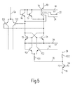
In Fig. 5 ist eine Abwandlung der Schaltung nach Fig. 3 dargestellt, bei der der
Stromschalter durch zwei PNP-Transistoren T21 und T22 realisiert ist, deren Basen
ebenfalls direkt von den Kollektoren der Transistoren T3 und T4 angesteuert
werden. Wenn angenommen wird, daß die Bezugsspannung U1 = 1,5 V ist und die
Sättigungsspannung der Transistoren T3 und T4 ca. 0 V sowie als minimale
Kollektor-Basis-Spannung UCD der Transistoren T21 und T22 0 V zugelassen wird,
dann ist die maximal mögliche Kollektorspannung an den Transistoren T21 und T22
im wesentlichen gleich U1, d.h. gleich 1,5 V. Sollen höhere Werte möglich sein,
müssen die Bezugsspannung U1 und die Betriebsspannung U2 und der Maximalwert
des Datensignals am Dateneingang 16 entsprechend erhöht werden. Im Layout
gemäß Fig. 4 kann der Transistor T21 mit den Transistoren T4 und TS1 sowie der
Transistor T22 mit den Transistoren T3 und TS2 unter gewissen Bedingungen in
jeweils eine gemeinsame Insel gelegt werden. Die von den Transistoren T3 und T4
ausgelösten parasitären Ströme in den Kollektoren der Transistoren T21 und T22
müssen dabei durch dazwischen liegende p-dotierte Streifen reduziert werden, und
der verbleibende Resteinfluß muß innerhalb der Genauigkeitsanforderungen des
D/A-Wandlers liegen. 5 shows a modification of the circuit according to FIG. 3, in which the
Current switch is realized by two PNP transistors T21 and T22, whose bases
also directly controlled by the collectors of transistors T3 and T4
will. If it is assumed that the reference voltage U1 = 1.5 V and the
Saturation voltage of transistors T3 and T4 approx. 0 V and as a minimum
Collector base voltage UCD of transistors T21 and T22 0 V is permitted,
then the maximum possible collector voltage at transistors T21 and T22
essentially equal to U1, i.e. equal to 1.5 V. Should higher values be possible,
must have the reference voltage U1 and the operating voltage U2 and the maximum value
of the data signal at the
Ein weiteres Ausführungsbeispiel ist in Fig. 6 dargestellt. Darin ist nur ein
Steuertransistor TS3 vorhanden, dessen Basis über den Widerstand R24 von der
Steuerleitung 14 und dessen Emitter über den Widerstand R23 von dem Datensignal
16 angesteuert wird. Weiterhin ist in der Verbindung zwischen dem Kollektor des
Transistors T4 und der Basis des Transistors T3 ein Widerstand R25 angeordnet.
Andererseits sind die Kollektoren der Transistoren T3 und T4 nicht mehr über
Dioden mit der Betriebsspannung U2 auf der Leitung 18 verbunden. Diese
Betriebsspannung U2 kann daher auch um mehr als Ube höher sein als die
Bezugsspannung U1 auf der Leitung 28. Diese Schaltung arbeitet wie folgt.Another embodiment is shown in FIG. 6. There is only one in it
Control transistor TS3 is present, the base of which is connected via resistor
Wenn das Signal am Steuereingang 14 niedrig ist, ist der Transistor TS3 gesperrt
und beeinflußt nicht den Zustand des Flipflops. Zum Einschreiben erhält der
Steuereingang 14 ein höheres Signal, beispielsweis 4 V oder größer, wenn
vorausgesetzt ist, daß die Bezugsspannung U1 auf der Leitung einen Wert von 1,5 V
hat. Der Stromfluß im Kollektor des Transistors TS3 hängt nun vom Signal am
Dateneingang 16 ab. Wenn dieses Signal hoch ist, fließt durch den Widerstand R23
und den Emitter des Transistors TS3 kein Strom. Der Kollektor des Transistors TS3
liegt je nach Zustand des Flipflops auf nahezu der Bezugsspannung U1 oder um Ube
höher, d.h. in jedem Fall auf einer niedrigeren Spannung als die Emitterspannung
und die Basisspannung des Transistors TS3. Wenn vorausgesetzt wird, daß das
Signal am Dateneingang 16 höher ist als das Signal am Steuereingang 14, wird der
Transistor TS3 invers leitend. Damit fließt nun ein Strom vom Kollektor des
Transistors TS3 zur Basis des Transistors T3 und durch den Widerstand R25. Wenn
angenommen wird, daß vorher der Transistor T4 leitend war, so erhöht sich nun die
Basisspannung am Transistor T3 so weit, daß dieser leitend wird und nun seinerseits
den Transistor T4 sperrt. Das Flipflop wird so in einen neuen Zustand gebracht. Die
Basis des Transistors T3 liegt nun auf einer Spannung von
Für den anderen einzuschreibenden Datenwert ist das Signal am Dateneingang 16
gleich Null. Dann fließt, wenn das Signal am Steuereingang 14 hoch ist, durch den
Widerstand R24 ein Basisstrom in den Transistor TS3 und somit auch ein
Emitterstrom durch den Widerstand R23. Dadurch wird der Transistor TS3
praktisch gesättigt leitend, und es fließt ein Strom durch den Widerstand R25 in den
Kollektor von TS3, der die Basis des Transistors T3 auf eine niedrigere Spannung
zieht. Wenn vorher der Transistor T3 leitend war, wird er nun dadurch gesperrt,
und der Transistor T4 wird leitend. Damit ist das Flipflop in einen anderen Zustand
gebracht. Wenn das Signal am Steuereingang 14 wieder niedrig wird, wird der
Transistor TS3 gesperrt, und der Zustand des Flipflops bleibt erhalten.For the other data value to be written in, the signal at data input is 16
equals zero. Then, when the signal at the
Diese Ausführungsform hat gegenüber den Schaltungen nach Fig. 3 und Fig. 5 den
Vorteil, daß eine Komponente weniger benötigt wird, nämlich nur ein
Steuertransistor, und die Betriebsspannung U2 auf der Leitung 18 zu höheren
Werten frei gewählt werden kann. Damit kann der Transistor T5 Teil einer
PNP-Bank sein, wobei der Emitter dann an eine positive Versorgungsspannung
angeschlossen ist. Andererseits ist die Realisierung im Layout in der Weise
aufwendiger, daß der Transistor TS3 in einer separaten Insel angeordnet sein muß.
Die Transistoren R23 und R24 können in der Insel für den Transistor T5 angeordnet
sein, wenn für die Betriebsspannung U2 auf der Leitung 18 eine Spannung gewählt
wird, die größer ist als das maximale Steuersignal auf der Leitung 14. Damit ist
gegenüber dem in Fig. 4 dargestellten Layout eine Insel mehr, nämlich sechs Inseln
erforderlich, wodurch der Vorteil des geringeren Komponentenaufwandes wieder
verringert wird.This embodiment has compared to the circuits of FIG. 3 and FIG
Advantage that one component is needed less, namely only one
Control transistor, and the operating voltage U2 on
In der Schaltung nach Fig. 6 können die Transistoren T1 und T2 für den Stromschalter auch wieder als PNP-Transistoren ausgeführt werden.6, the transistors T1 and T2 for the Current switches can also be designed as PNP transistors.
Claims (6)
dadurch gekennzeichnet,
characterized by
Applications Claiming Priority (2)
| Application Number | Priority Date | Filing Date | Title |
|---|---|---|---|
| DE19651921 | 1996-12-13 | ||
| DE19651921 | 1996-12-13 |
Publications (3)
| Publication Number | Publication Date |
|---|---|
| EP0848499A2 true EP0848499A2 (en) | 1998-06-17 |
| EP0848499A3 EP0848499A3 (en) | 2001-02-28 |
| EP0848499B1 EP0848499B1 (en) | 2003-05-21 |
Family
ID=7814629
Family Applications (1)
| Application Number | Title | Priority Date | Filing Date |
|---|---|---|---|
| EP97203786A Expired - Lifetime EP0848499B1 (en) | 1996-12-13 | 1997-12-03 | Circuit arrangement for a memory cell in a D/A converter |
Country Status (4)
| Country | Link |
|---|---|
| US (1) | US6005792A (en) |
| EP (1) | EP0848499B1 (en) |
| JP (1) | JP3872193B2 (en) |
| DE (1) | DE59710118D1 (en) |
Families Citing this family (1)
| Publication number | Priority date | Publication date | Assignee | Title |
|---|---|---|---|---|
| JP2003521113A (en) * | 2000-01-19 | 2003-07-08 | コーニンクレッカ フィリップス エレクトロニクス エヌ ヴィ | Reference voltage source for bandgap voltage |
Citations (3)
| Publication number | Priority date | Publication date | Assignee | Title |
|---|---|---|---|---|
| US4210830A (en) * | 1978-08-28 | 1980-07-01 | Precision Monolithics, Inc. | High speed switching circuit |
| US4383248A (en) * | 1981-12-21 | 1983-05-10 | Motorola, Inc. | Latchable fast settling digital to analog converter bit switch |
| US4563669A (en) * | 1983-01-31 | 1986-01-07 | Siemens Aktiengesellschaft | Integrated digital/analog converter |
Family Cites Families (1)
| Publication number | Priority date | Publication date | Assignee | Title |
|---|---|---|---|---|
| US5321401A (en) * | 1992-12-04 | 1994-06-14 | Texas Instruments Incorporated | Method and apparatus for digital to analog conversion with minimized distortion |
-
1997
- 1997-12-03 EP EP97203786A patent/EP0848499B1/en not_active Expired - Lifetime
- 1997-12-03 DE DE59710118T patent/DE59710118D1/en not_active Expired - Lifetime
- 1997-12-11 US US08/988,593 patent/US6005792A/en not_active Expired - Lifetime
- 1997-12-15 JP JP34506497A patent/JP3872193B2/en not_active Expired - Fee Related
Patent Citations (3)
| Publication number | Priority date | Publication date | Assignee | Title |
|---|---|---|---|---|
| US4210830A (en) * | 1978-08-28 | 1980-07-01 | Precision Monolithics, Inc. | High speed switching circuit |
| US4383248A (en) * | 1981-12-21 | 1983-05-10 | Motorola, Inc. | Latchable fast settling digital to analog converter bit switch |
| US4563669A (en) * | 1983-01-31 | 1986-01-07 | Siemens Aktiengesellschaft | Integrated digital/analog converter |
Also Published As
| Publication number | Publication date |
|---|---|
| EP0848499A3 (en) | 2001-02-28 |
| JP3872193B2 (en) | 2007-01-24 |
| JPH10200410A (en) | 1998-07-31 |
| DE59710118D1 (en) | 2003-06-26 |
| US6005792A (en) | 1999-12-21 |
| EP0848499B1 (en) | 2003-05-21 |
Similar Documents
| Publication | Publication Date | Title |
|---|---|---|
| DE2423478C3 (en) | Power source circuit | |
| DE2160432C3 (en) | Constant voltage circuit | |
| DE2207233C3 (en) | Electronic signal amplifier | |
| DE3937501A1 (en) | METHOD AND DEVICE FOR GENERATING A PRELOAD | |
| DE1762172B2 (en) | LINK SWITCH WITH POWER TRANSFER SWITCHES | |
| DE2260405A1 (en) | REFERENCE VOLTAGE GENERATOR CIRCUIT | |
| DE3419664A1 (en) | CURRENT MIRROR SWITCHING | |
| DE2429771A1 (en) | STORAGE MATRIX WITH CONTROLLABLE FOUR-LAYER SEMI-CONDUCTORS | |
| DE2416534B2 (en) | TRANSISTOR CIRCUIT FOR REVERSING THE DIRECTION OF CURRENT IN A CONSUMER | |
| DE3501274C2 (en) | ||
| DE3615383C2 (en) | A circuit for shifting the input level of a digital-to-analog converter | |
| DE2924171C2 (en) | ||
| DE1901808A1 (en) | Circuit arrangement for performing logical functions | |
| DE69532061T2 (en) | Amplifier circuit and method | |
| DE19547754C1 (en) | Control circuit for BiCMOS bus driver | |
| EP0848499B1 (en) | Circuit arrangement for a memory cell in a D/A converter | |
| DE4321483C2 (en) | Line driver switching stage in current switch technology | |
| EP0134270B1 (en) | Latched phase splitter | |
| DE1948178C3 (en) | A monolithic semiconductor circuit consisting of a large number of individual logic circuits with an integrated DC voltage stabilization semiconductor circuit | |
| DE3716577C2 (en) | Current mirror circuit of great performance | |
| DE3615382C2 (en) | Digital-to-analog converter with a bit setting and filter circuit | |
| DE3335133C2 (en) | ||
| EP0588111B1 (en) | Memory element | |
| DE1814887C3 (en) | Transistor amplifier | |
| EP0413038B1 (en) | Two-phase bipolar shift register |
Legal Events
| Date | Code | Title | Description |
|---|---|---|---|
| PUAI | Public reference made under article 153(3) epc to a published international application that has entered the european phase |
Free format text: ORIGINAL CODE: 0009012 |
|
| AK | Designated contracting states |
Kind code of ref document: A2 Designated state(s): DE FR GB IT NL |
|
| AX | Request for extension of the european patent |
Free format text: AL;LT;LV;MK;RO;SI |
|
| RAP3 | Party data changed (applicant data changed or rights of an application transferred) |
Owner name: KONINKLIJKE PHILIPS ELECTRONICS N.V. Owner name: PHILIPS PATENTVERWALTUNG GMBH |
|
| RAP3 | Party data changed (applicant data changed or rights of an application transferred) |
Owner name: KONINKLIJKE PHILIPS ELECTRONICS N.V. Owner name: PHILIPS CORPORATE INTELLECTUAL PROPERTY GMBH |
|
| PUAL | Search report despatched |
Free format text: ORIGINAL CODE: 0009013 |
|
| AK | Designated contracting states |
Kind code of ref document: A3 Designated state(s): AT BE CH DE DK ES FI FR GB GR IE IT LI LU MC NL PT SE |
|
| AX | Request for extension of the european patent |
Free format text: AL;LT;LV;MK;RO;SI |
|
| 17P | Request for examination filed |
Effective date: 20010828 |
|
| AKX | Designation fees paid |
Free format text: DE FR GB IT NL |
|
| GRAH | Despatch of communication of intention to grant a patent |
Free format text: ORIGINAL CODE: EPIDOS IGRA |
|
| RAP1 | Party data changed (applicant data changed or rights of an application transferred) |
Owner name: KONINKLIJKE PHILIPS ELECTRONICS N.V. Owner name: PHILIPS CORPORATE INTELLECTUAL PROPERTY GMBH |
|
| GRAH | Despatch of communication of intention to grant a patent |
Free format text: ORIGINAL CODE: EPIDOS IGRA |
|
| GRAA | (expected) grant |
Free format text: ORIGINAL CODE: 0009210 |
|
| RAP1 | Party data changed (applicant data changed or rights of an application transferred) |
Owner name: KONINKLIJKE PHILIPS ELECTRONICS N.V. Owner name: PHILIPS INTELLECTUAL PROPERTY & STANDARDS GMBH |
|
| AK | Designated contracting states |
Designated state(s): DE FR GB IT NL |
|
| PG25 | Lapsed in a contracting state [announced via postgrant information from national office to epo] |
Ref country code: NL Free format text: LAPSE BECAUSE OF FAILURE TO SUBMIT A TRANSLATION OF THE DESCRIPTION OR TO PAY THE FEE WITHIN THE PRESCRIBED TIME-LIMIT Effective date: 20030521 Ref country code: IT Free format text: LAPSE BECAUSE OF FAILURE TO SUBMIT A TRANSLATION OF THE DESCRIPTION OR TO PAY THE FEE WITHIN THE PRESCRIBED TIME-LIMIT;WARNING: LAPSES OF ITALIAN PATENTS WITH EFFECTIVE DATE BEFORE 2007 MAY HAVE OCCURRED AT ANY TIME BEFORE 2007. THE CORRECT EFFECTIVE DATE MAY BE DIFFERENT FROM THE ONE RECORDED. Effective date: 20030521 |
|
| REG | Reference to a national code |
Ref country code: GB Ref legal event code: FG4D Free format text: NOT ENGLISH |
|
| REF | Corresponds to: |
Ref document number: 59710118 Country of ref document: DE Date of ref document: 20030626 Kind code of ref document: P |
|
| GBT | Gb: translation of ep patent filed (gb section 77(6)(a)/1977) |
Effective date: 20030730 |
|
| NLV1 | Nl: lapsed or annulled due to failure to fulfill the requirements of art. 29p and 29m of the patents act | ||
| ET | Fr: translation filed | ||
| PLBE | No opposition filed within time limit |
Free format text: ORIGINAL CODE: 0009261 |
|
| STAA | Information on the status of an ep patent application or granted ep patent |
Free format text: STATUS: NO OPPOSITION FILED WITHIN TIME LIMIT |
|
| 26N | No opposition filed |
Effective date: 20040224 |
|
| REG | Reference to a national code |
Ref country code: GB Ref legal event code: 746 Effective date: 20040811 |
|
| REG | Reference to a national code |
Ref country code: FR Ref legal event code: D6 |
|
| REG | Reference to a national code |
Ref country code: GB Ref legal event code: 732E |
|
| REG | Reference to a national code |
Ref country code: FR Ref legal event code: TP |
|
| PGFP | Annual fee paid to national office [announced via postgrant information from national office to epo] |
Ref country code: GB Payment date: 20091202 Year of fee payment: 13 Ref country code: FR Payment date: 20091221 Year of fee payment: 13 |
|
| PGFP | Annual fee paid to national office [announced via postgrant information from national office to epo] |
Ref country code: DE Payment date: 20091126 Year of fee payment: 13 |
|
| GBPC | Gb: european patent ceased through non-payment of renewal fee |
Effective date: 20101203 |
|
| REG | Reference to a national code |
Ref country code: FR Ref legal event code: ST Effective date: 20110831 |
|
| PG25 | Lapsed in a contracting state [announced via postgrant information from national office to epo] |
Ref country code: FR Free format text: LAPSE BECAUSE OF NON-PAYMENT OF DUE FEES Effective date: 20110103 |
|
| REG | Reference to a national code |
Ref country code: DE Ref legal event code: R119 Ref document number: 59710118 Country of ref document: DE Effective date: 20110701 |
|
| PG25 | Lapsed in a contracting state [announced via postgrant information from national office to epo] |
Ref country code: GB Free format text: LAPSE BECAUSE OF NON-PAYMENT OF DUE FEES Effective date: 20101203 Ref country code: DE Free format text: LAPSE BECAUSE OF NON-PAYMENT OF DUE FEES Effective date: 20110701 |