EP0843375A1 - Nonreciprocal circuit device - Google Patents
Nonreciprocal circuit device Download PDFInfo
- Publication number
- EP0843375A1 EP0843375A1 EP97119922A EP97119922A EP0843375A1 EP 0843375 A1 EP0843375 A1 EP 0843375A1 EP 97119922 A EP97119922 A EP 97119922A EP 97119922 A EP97119922 A EP 97119922A EP 0843375 A1 EP0843375 A1 EP 0843375A1
- Authority
- EP
- European Patent Office
- Prior art keywords
- ferromagnetic body
- ferromagnetic
- circuit device
- central conductors
- nonreciprocal circuit
- Prior art date
- Legal status (The legal status is an assumption and is not a legal conclusion. Google has not performed a legal analysis and makes no representation as to the accuracy of the status listed.)
- Granted
Links
Images


Classifications
-
- H—ELECTRICITY
- H01—ELECTRIC ELEMENTS
- H01P—WAVEGUIDES; RESONATORS, LINES, OR OTHER DEVICES OF THE WAVEGUIDE TYPE
- H01P1/00—Auxiliary devices
- H01P1/32—Non-reciprocal transmission devices
- H01P1/38—Circulators
- H01P1/383—Junction circulators, e.g. Y-circulators
- H01P1/387—Strip line circulators
Definitions
- the present invention relates to a nonreciprocal circuit device for use in a mobile communications apparatus such as a portable telephone, etc., and particularly to a nonreciprocal circuit device used as a circulator or an isolator in a high frequency band such as the microwave band or the like.
- a known nonreciprocal circuit device is, for example, a device comprising a plurality of central electrodes arranged to cross each other in an electrically isolated state, microwave magnetic materials provided above and below the plurality of central electrodes, and a permanent magnet for applying a DC magnetic field to the plurality of central electrodes, i.e., a lumped-parameter nonreciprocal circuit device.
- a lumped-parameter nonreciprocal circuit device is used as, for example, a circulator or an isolator.
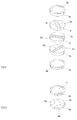
- Fig. 1 is an exploded perspective view showing an example of a conventional circulator.
- this circulator in order to decrease the size thereof, a plurality of central conductors are arranged in a ferromagnetic body 1 to cross each other in an electrically isolated state.
- the ferromagnetic body 1 has a laminated structure comprising a plurality of ferromagnetic material layers 1a to 1e.
- On the upper sides of the ferromagnetic material layers 1b, 1c and 1d are formed central conductors 2a and 2b, 2c and 2d and 2e and 2f, respectively.
- a pair of central conductors On the upper side of each of the ferromagnetic material layers 1b to 1d are arranged a pair of central conductors.
- the central conductors 2a and 2b, the central conductors 2c and 2d, and the central conductors 2e and 2f are arranged to cross each other in a laminated state, and are electrically isolated by the ferromagnetic material layers 1c and 1d.
- earth electrodes 3a and 3b On the ferromagnetic material layers 1a and 1e are formed earth electrodes 3a and 3b, respectively.
- external electrodes 4a, 4b and 4c are formed on the side thereof so as to be connected to the earth electrodes 3a and 3b in common, and each external electrode being electrically connected to the ends of one of the pairs of central conductors 2a - 2f.
- the dielectric body 5 comprises dielectric ceramic and has a capacitor provided therein for forming a matching circuit. Namely, as shown in an exploded view of Fig. 3, the dielectric body 5 has a laminated structure comprising dielectric layers 5a and 5b. On the upper side of the dielectric layer 5a are formed capacity electrodes 6a, 6b and 6c. On the upper side of the dielectric layer 5b is formed an earth electrode 7. Therefore, in each portion where the capacity electrodes 6a to 6c are overlapped with the earth electrode 7 and the earth electrode 3b through the dielectric layers 5b and 5a, respectively, a capacitor is formed.
- external electrodes 8a, 8b and 8c are formed on the side of the dielectric body 5. Each of these external electrodes 8a to 8c is electrically connected to one of the capacity electrodes or one of the earth electrodes.
- the ferromagnetic body 1 and the dielectric body 5 are contained in a terminal plate 9 having a cylindrical concave 9a at the center thereof.
- conductor patterns 10a to 10c which constitute input/output terminals
- conductive patterns 10d, 10e and 10f which are connected to the earth potential.
- the external electrodes 4a to 4c formed on the side of the ferromagnetic body 1 and the external electrodes 8a to 8c formed on the side of the dielectric body 5 are contained in the concave 9a of the terminal plate 9 and appropriately connected to the conductive patterns 10a to 10f.
- a permanent magnet 11 is provided for applying a magnetic field to a portion in the ferromagnetic body 1 where the central conductors cross each other.
- the nonreciprocal circuit device shown in Fig. 1 further comprises metallic yokes 12 and 13.
- the terminal plate 9 and the magnet 11 are held between the yokes 12 and 13.
- the yokes 12 and 13 constitute a magnetic circuit for applying a magnetic field together with the magnet 11.
- the nonreciprocal circuit device shown in Figs. 1 to 3 since the portion where the plurality of central conductors 2a, 2b to 2e and 2f cross each other in an electrically isolated state is integrally formed by using the ferromagnetic body 1, the nonreciprocal circuit device can easily be manufactured, and miniaturized.
- the ferromagnetic body 1 and the dielectric body 5 are separately fired and then joined together, the external electrodes 4a to 4c and the external electrodes 8a to 8c on the sides thereof must be electrically connected by soldering or the like. Therefore, the number of the connection points is increased, and thus, a problem occurs with respect to insufficient reliability. Also, since the ferromagnetic body 1 and the dielectric body 5 are fired separately, a plurality of firing steps must be carried out, and a troublesome assembly process is required, thereby making it difficult to reduce the manufacturing cost.
- the above problems can be possibly solved by simultaneously firing the ferromagnetic body 1 and the dielectric body 5. Namely, the above problems can be possibly solved by a method in which a green sheet for forming the ferromagnetic body 1 and a green sheet for forming the dielectric body 5 are laminated and simultaneously fired.
- firing conditions for the ferromagnetic body 1 and the dielectric body 5 are different, and thus firing under conditions suitable for one of the bodies causes the possibility that firing of the other does not sufficiently proceed. Also firing under conditions intermediate between the conditions for both bodies causes a problem in that both the ferromagnetic body 1 and the dielectric body 5 may not be properly fired.
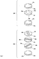
- Fig. 4 is an exploded perspective view illustrating another example of a conventional nonreciprocal circuit device.
- a plurality of central conductors and a matching circuit are arranged in the ferromagnetic body 15 shown in Fig. 4.
- the electrode structure in the ferromagnetic body 15 is shown in an exploded perspective view of Fig. 5.
- ferromagnetic layers 15a to 15e are laminated.
- ferromagnetic layers 15b to 15d are formed on the upper sides of the ferromagnetic layers 15b to 15d.
- a plurality of central conductors 16a, 16b to 16e and 16f are formed on the upper sides of the ferromagnetic layers 15b to 15d.
- ends of the central conductors 16a and 16b on the upper surface of the ferromagnetic layer 15b are electrically connected to a capacity electrode 17a.
- ends of the central conductors 16c and 16d on the upper side of the ferromagnetic layer 15c are connected to a capacity electrode 17b formed thereon, and ends of the central conductors 16e and 16f on upper side of the ferromagnetic layer 15d are electrically connected to a capacity electrode 17c formed thereon.
- earth electrodes 18a and 18b On the upper sides of the ferromagnetic layers 15a and 15e are formed earth electrodes 18a and 18b, respectively. Therefore, in the ferromagnetic material 15 formed by laminating the ferromagnetic layers 15a to 15e and integrally firing the layers, not only the plurality of central conductors 16a to 16f are arranged, but also the capacity electrodes 17a to 17c for forming a matching circuit are arranged. The capacity electrodes 17a to 17c are overlapped with the earth electrodes 18a and 18b to form capacitors.
- the ferromagnetic body 15 is inserted into a concave 9a of a terminal plate 9 with a permanent magnet 11 disposed thereon, and held between metallic yokes 12 and 13 to form a nonreciprocal circuit device.
- the nonreciprocal circuit device shown in Fig. 4 comprises the portion where the plurality of central conductors are arranged by using the ferromagnetic body 15, and the matching circuit. Therefore, the assembly step can be simplified, and the manufacturing cost can be decreased because a plurality of lines need not be used in the raw material preparing step. Also, since there is no need for joining the central conductors and the matching circuit by soldering or the like, the reliability can be improved.
- the capacitors for forming the matching circuit are formed by the ferromagnetic body 15, it is possible that a loss in the matching circuit may be increased due to the magnetic loss of the ferromagnetic body, whereby the insertion loss of the nonreciprocal circuit device may be increased.
- the present invention is able to remove the above faults of the prior art, and provide a nonreciprocal circuit device with excellent reliability which permits reduction in its size and simplification of its manufacturing process without deterioration in its properties, such as insertion loss.
- a nonreciprocal circuit device comprising a first ferromagnetic body, a plurality of central conductors which are formed in the first ferromagnetic body and which are arranged to cross each other in an electrically isolated state, a second ferromagnetic body fixed to the first ferromagnetic body, and a matching circuit formed in the second ferromagnetic body and electrically connected to the plurality of central conductors, wherein the first and second ferromagnetic bodies have different saturation magnetizations.
- the first ferromagnetic body and the second ferromagnetic body are integrally formed, the plurality of central conductors are arranged in the first ferromagnetic body, and the matching circuit is provided in the second ferromagnetic body.
- the portion where the plurality of central conductors are arranged and the portion where the matching circuit is formed both comprise ferromagnetic bodies, and thus the same line can be used in the raw material preparing step.
- the magnetic loss can be decreased both when the saturation magnetization of the second ferromagnetic body is smaller than that of the first ferromagnetic body, and when the saturation magnetization of the second ferromagnetic body is larger than that of the first ferromagnetic body.
- a magnetic circuit is preferably provided on the first ferromagnetic body in order to apply a DC magnetic field.
- the assembly step can further be simplified.
- the matching circuit comprises plural pairs of capacity electrodes and earth electrodes which are formed to hold the magnetic layers of the second ferromagnetic body therebetween.
- the pairs of capacity electrodes respectively form the capacitors each of which is electrically connected to any one of the plurality of central conductors.
- first and second ferromagnetic bodies are preferably integrated by simultaneous firing. Therefore, the step of fixing the first and second ferromagnetic bodies can be omitted, thereby increasing the reliability of the electric connection between the central conductors and the matching circuit.
- Fig. 6 is an exploded perspective view of a nonreciprocal circuit device in accordance with an embodiment of the present invention.
- the construction shown in Fig. 6 is the same as the conventional nonreciprocal circuit device shown in Fig. 4 except for the structure of a ferromagnetic body 25.
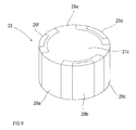
- Fig. 7 is an exploded perspective view of the ferromagnetic body 25.
- the ferromagnetic body 25 has a structure in which ferromagnetic layers 25a to 25g are laminated and integrally fired.
- the ferromagnetic layers 25a to 25d constitute a first ferromagnetic body 25A
- the ferromagnetic layers 25e to 25g constitute a second ferromagnetic body 25B.
- each central conductor extending in a given direction comprises a pair of central conductors, as described above.
- the central conductors 26a and 26b, the central conductors 26c and 26d, and the central conductors 26e and 26f are arranged so as to cross each other in the vicinity of the center. Also the central conductors 26a and 26b, the central conductors 26c and 26d, and the central conductors 26e and 26f are arranged with the ferromagnetic layers 25c and 25d, respectively, therebetween, and thus electrically isolated.
- earth electrodes 27a, 27b and 27c On the upper surfaces of the ferromagnetic layers 25a, 25e and 25g are formed earth electrodes 27a, 27b and 27c, respectively. On the upper surface of the ferromagnetic layer 25f are formed three capacity electrodes 28a, 28b and 28c. The capacity electrodes 28a to 28c are opposed to the earth electrodes 27b and 27c through the ferromagnetic layers 25f and 25g, respectively, to form three capacitors.
- the central conductors 26a to 26f, the earth electrodes 27a to 27c and the capacity electrodes 28a to 28c are formed by coating conductive paste on the upper surfaces of magnetic green sheets, laminating the green sheets, and then integrally firing the green sheets.
- the ferromagnetic body 25 comprises an integrally sintered compact.
- external electrodes 29a to 29f are formed on the side of the ferromagnetic body 25.
- the external electrodes 29a, 29c and 29e are connected to the earth electrodes 27a, 27b and 27c.
- the external electrode 29a is also connected to ends of the central conductors 26a and 26b.
- the external electrode 29c is connected to ends of the central conductors 26c and 26d.
- the external electrode 29e is electrically connected to ends of the central conductors 26e and 26f, i.e., the ends to be connected to the earth potential.
- the external electrode 29b is connected to the other ends of the central conductors 26e and 26f.
- the external electrodes 29d and 29f are connected to the other ends of the central conductors 26a and 26b and the central conductors 26c and 26d, respectively.
- the external electrodes 29b, 29c and 29f are electrically connected to the capacity electrodes 28c, 28b and 28a, respectively.
- the external electrodes 29b, 29d and 29f constitute portions to be connected to an input/output terminal, and the external electrodes 29a, 29c and 29e constitute connecting ends to be connected to the earth electrodes.
- the external electrodes 29a to 29f are formed by coating conductive paste on the ferromagnetic body 25 obtained by integral firing, and then hardening or baking the conductive paste.
- the external electrodes 29a to 29f may be completed by laminating magnetic green sheets before firing, coating conductive paste on the side of the laminate and then integrally firing it to fire the magnetic material and bake the external electrodes 29a to 29f.
- the ferromagnetic body 25 of this embodiment contains not only the plurality of central conductors 26a to 26f and the earth electrodes 27a and 27b, but also the capacity electrodes 28a to 28c and the earth electrode 27c for forming a matching circuit.
- the capacity electrodes 28a to 28c and the earth electrode 27c for forming a matching circuit.
- the portion where the matching circuit is formed also comprises the ferromagnetic material, raw materials can be prepared by using the same line, and thus the matching circuit cost can be reduced.
- the saturation magnetization of the second ferromagnetic body 25B comprising the magnetic layers 25e to 25g is lower than the saturation magnetization of the first ferromagnetic body 25A comprising the magnetic layers of the portion where the central conductors are arranged, i.e., the magnetic layers 25a to 25d. Therefore, it is possible to reduce the magnetic material loss of the matching circuit.
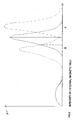
- Fig. 9 shows the characteristics of the imaginary part ( ⁇ +'') of the permeability for a positive circularly polarized wave to an external magnetic field.
- a solid line shows ⁇ +'' of the magnetic body which constitutes the central conductors
- a broken line shows ⁇ +'' of the ferromagnetic body with lower saturation magnetization which constitutes the matching circuit. Since the imaginary part of the permeability for a negative circularly polarized wave is close to zero, the magnetic material loss of the ferromagnetic material is proportional to the intensity of the imaginary part ⁇ +'' of permeability for a positive circularly polarized wave.
- a nonreciprocal circuit device is generally formed so as to operate in the region A shown in Fig. 9. Therefore, it can be found that since the saturation magnetization of the second ferromagnetic body which forms the matching circuit is made lower than the saturation magnetization of the first ferromagnetic body where the central conductors are arranged, the magnetic material loss of the matching circuit can be reduced.
- each of the first and second ferromagnetic bodies 25A and 25B comprises, for example, microwave ferrite such as yttrium iron garnet or calcium-vanadium garnet, represented by Y 3 Fe 5-z Al z O 12 or ⁇ Ca 3-y Y y ⁇ [Fe 2 ] (Fe 1.5+0.5y-z Al z V 1.5-0.5y )O 12 (0 ⁇ Z ⁇ 1.0, 0 ⁇ Y ⁇ 3.0).
- the saturation magnetization of the second ferromagnetic body 25B can be decreased by relatively increasing the amount of Al (the Z value) in the microwave ferrite.
- the saturation magnetization of the second ferromagnetic body is lower than the saturation magnetization of the first ferromagnetic body
- the saturation magnetization of the second ferromagnetic body may be larger than that of the first ferromagnetic body.
- the magnetic material loss can be decreased in a similar manner to the above embodiment, i.e., the magnetic material loss of the matching circuit can be decreased by making the saturation magnetization of the ferromagnetic body which forms the matching circuit larger than that of the first ferromagnetic body. It can thus be found that the ⁇ +'' of the second ferromagnetic body which forms the matching circuit is as shown by a one-dot chain line in Fig. 9, and the magnetic material loss is decreased in the region B.
- the saturation magnetization of either of the first and second ferromagnetic bodies may be increased. In both cases, the magnetic material loss of the matching circuit can be effectively reduced.
- the nonreciprocal circuit device of this embodiment comprises the ferromagnetic body 25 which is contained in the concave 9a of the terminal plate 9 and electrically connected to conductive patterns 10a to 10f formed on the terminal plate 9. Since the terminal plate 9 of this embodiment is the same as the terminal plate 9 shown in Fig. 1, the corresponding portions are denoted by corresponding reference numerals, and the description thereof is omitted.
- a permanent magnet 11 On the ferromagnetic body 25 is fixed a permanent magnet 11.
- the permanent magnet 11 an appropriate permanent magnet comprising ferrite or the like can be used.
- metallic yokes 12 and 13 together with the permanent magnet, apply a magnetic field to the portion where the central conductors cross each other.
- the ferromagnetic body 25 may further comprise a magnetic circuit for applying a magnetic field to the portion where the central conductors cross each other.
- a coiled conductive pattern may be integrally formed in the ferromagnetic body so that a magnetic field is generated by supplying the coiled conductive pattern with electricity.
- each central conductor formed at a given level comprises a pair of central conductors, e.g., the central conductors 26a and 26b, as shown in Fig. 7, a single central conductor extending in a given direction at a given level may be provided.
- the plurality of central conductors are formed in the first ferromagnetic body, and the matching circuit is formed in the second ferromagnetic body, dielectric materials which are fired under completely different firing conditions need not be used, and thus the firing conditions need not be greatly changed even when the first and second ferromagnetic bodies are fired separately. Also the number of the raw materials prepared can be reduced, and the manufacturing cost can thus be reduced.
- the magnetic material loss of the matching circuit can be reduced. It is thus possible to provide a small, low-priced nonreciprocal circuit device having low insertion loss.
- a magnetic circuit is integrally formed for applying a DC magnetic field to the first ferromagnetic body
- means for applying a magnetic field to the central conductors can also be integrally provided, and a smaller nonreciprocal circuit device with excellent reliability can thus be provided.
- the capacity electrodes are formed on magnetic material green sheets and then fired. It is thus possible to easily form each of the capacitors for forming the matching circuit in the second ferromagnetic body by a ceramic firing technique.
- first and second ferromagnetic bodies are integrated by simultaneous firing, there is no need for the work of fixing the first and second ferromagnetic bodies, and thus a nonreciprocal circuit device having more excellent reliability can be obtained. Also, since the first and second ferromagnetic bodies need not be fired separately, the manufacturing process can significantly be simplified, and the same line can be used in the raw material preparing step, thereby significantly decreasing the manufacturing cost.
Abstract
Description
- Fig. 1
- is an exploded perspective view illustrating an example of a conventional nonreciprocal circuit device;
- Fig. 2
- is an exploded perspective view of the ferromagnetic body shown in Fig. 1;
- Fig. 3
- is an exploded perspective view illustrating the internal structure of the dielectric body shown in Fig. 1;
- Fig. 4
- is an exploded perspective view illustrating another example of a conventional nonreciprocal circuit device;
- Fig. 5
- is an exploded perspective view illustrating the internal structure of the ferromagnetic body in the conventional nonreciprocal circuit device shown in Fig. 4;
- Fig. 6
- is an exploded perspective view illustrating a nonreciprocal circuit device in accordance with an embodiment of the present invention;
- Fig. 7
- is an exploded perspective view illustrating the ferromagnetic body used in the embodiment;
- Fig. 8
- is a perspective view illustrating the appearance of the ferromagnetic body used in the embodiment; and
- Fig. 9
- is a drawing showing the relation between an external magnetic field and the imaginary part µ+'' of the permeability for a positive circularly polarized wave, for illustrating the reason why the magnetic loss is decreased in the nonreciprocal circuit device of the embodiment.
Claims (6)
- A nonreciprocal circuit device comprising:a first ferromagnetic body (25A);a plurality of central conductors (26a, 26b, 26c, 26d, 26e, 26f) formed in the first ferromagnetic body (25A) and arranged to cross each other in an electrically isolated state;a second ferromagnetic body (25B) fixed to the first ferromagnetic body (25A); anda matching circuit (28a, 28b, 28c, 27c) formed in the second ferromagnetic body (25B) and electrically connected to the plurality of central conductors;
wherein the first and second ferromagnetic bodies (25A, 25B) have different saturation magnetizations. - A nonreciprocal circuit device according to Claim 1, wherein the saturation magnetization of the second ferromagnetic body (25B) is smaller than that of the first ferromagnetic body (25A).
- A nonreciprocal circuit device according to Claim 1, wherein the saturation magnetization of the second ferromagnetic body (25B) is larger than that of the first ferromagnetic body (25A).
- A nonreciprocal circuit device according to any one of Claims 1 to 3, further comprising a magnetic circuit (11, 12, 13) for applying a DC magnetic field to the first ferromagnetic body (25A).
- A nonreciprocal circuit device according to Claim 1, wherein the matching circuit has a plurality of pairs of capacity electrodes (28a, 28b, 28c, 27c) which are formed with magnetic material layers (25g) of the second ferromagnetic body (25B) therebetween, and each capacitor comprising a respective pair of capacity electrodes is electrically connected to a corresponding one of the plurality of central conductors (26a to 26f).
- A nonreciprocal circuit device according to any one of Claims 1 to 3, wherein the first and second ferromagnetic bodies (25A, 25B) comprise integrated and cofired magnetic material.
Applications Claiming Priority (3)
| Application Number | Priority Date | Filing Date | Title |
|---|---|---|---|
| JP08303196A JP3125693B2 (en) | 1996-11-14 | 1996-11-14 | Non-reciprocal circuit device |
| JP30319696 | 1996-11-14 | ||
| JP303196/96 | 1996-11-14 |
Publications (2)
| Publication Number | Publication Date |
|---|---|
| EP0843375A1 true EP0843375A1 (en) | 1998-05-20 |
| EP0843375B1 EP0843375B1 (en) | 2003-08-27 |
Family
ID=17918042
Family Applications (1)
| Application Number | Title | Priority Date | Filing Date |
|---|---|---|---|
| EP97119922A Expired - Lifetime EP0843375B1 (en) | 1996-11-14 | 1997-11-13 | Nonreciprocal circuit device |
Country Status (7)
| Country | Link |
|---|---|
| US (1) | US5926073A (en) |
| EP (1) | EP0843375B1 (en) |
| JP (1) | JP3125693B2 (en) |
| KR (1) | KR100278345B1 (en) |
| CN (1) | CN1114964C (en) |
| DE (1) | DE69724381T2 (en) |
| NO (1) | NO319870B1 (en) |
Cited By (5)
| Publication number | Priority date | Publication date | Assignee | Title |
|---|---|---|---|---|
| FR2806534A1 (en) * | 2000-02-25 | 2001-09-21 | Murata Manufacturing Co | NON-RECIPROCAL CIRCUIT DEVICE AND HIGH FREQUENCY CIRCUIT APPARATUS INCORPORATING THE SAME |
| EP1139486A1 (en) * | 2000-03-27 | 2001-10-04 | Hitachi Metals, Ltd. | Non-reciprocal circuit device and wireless communications equipment comprising the same |
| US7834716B2 (en) | 2007-08-22 | 2010-11-16 | Murata Manufacturing Co., Ltd. | Nonreciprocal circuit device |
| US7834717B2 (en) | 2007-08-22 | 2010-11-16 | Murata Manufacturing Co., Ltd. | Nonreciprocal circuit device |
| EP3057173A4 (en) * | 2013-10-11 | 2017-06-14 | Mitsubishi Electric Corporation | Non-reciprocal circuit |
Families Citing this family (10)
| Publication number | Priority date | Publication date | Assignee | Title |
|---|---|---|---|---|
| US6933799B1 (en) * | 1998-04-14 | 2005-08-23 | Tdk Corporation | Method of controlling intermodulation distortion of non-reciprocal device |
| US6215644B1 (en) | 1999-09-09 | 2001-04-10 | Jds Uniphase Inc. | High frequency tunable capacitors |
| US6496351B2 (en) | 1999-12-15 | 2002-12-17 | Jds Uniphase Inc. | MEMS device members having portions that contact a substrate and associated methods of operating |
| US6229684B1 (en) | 1999-12-15 | 2001-05-08 | Jds Uniphase Inc. | Variable capacitor and associated fabrication method |
| US6593833B2 (en) | 2001-04-04 | 2003-07-15 | Mcnc | Tunable microwave components utilizing ferroelectric and ferromagnetic composite dielectrics and methods for making same |
| US20030231076A1 (en) * | 2002-06-03 | 2003-12-18 | Matsushita Electric Industrial Co., Ltd. | Structure of non-reciprocal circuit element |
| JP4760981B2 (en) * | 2007-09-03 | 2011-08-31 | 株式会社村田製作所 | Non-reciprocal circuit element |
| CN101820799B (en) | 2007-10-09 | 2012-11-07 | 芭比特兰德公司 | Bedside sleeper for infants |
| KR20090111436A (en) * | 2008-04-22 | 2009-10-27 | 주식회사 이엠따블유안테나 | Ferrite structure and method for adjusting magnetic permeability of ferrite |
| US11699836B2 (en) * | 2018-06-21 | 2023-07-11 | Skyworks Solutions, Inc. | Low firing temperature dielectric materials designed to be co-fired with high bismuth garnet ferrites for miniaturized isolators and circulators |
Citations (4)
| Publication number | Priority date | Publication date | Assignee | Title |
|---|---|---|---|---|
| FR2111708A1 (en) * | 1970-10-19 | 1972-06-09 | Rca Corp | |
| JPS5767308A (en) * | 1980-10-14 | 1982-04-23 | Hitachi Metals Ltd | Lumped constant circulator and isolator |
| US4496915A (en) * | 1981-11-12 | 1985-01-29 | Trw Inc. | Microwave transmission device having gyromagnetic materials having different saturation magnetizations |
| EP0664573A1 (en) * | 1993-06-30 | 1995-07-26 | Murata Manufacturing Co., Ltd. | Non-reciprocal circuit element |
Family Cites Families (2)
| Publication number | Priority date | Publication date | Assignee | Title |
|---|---|---|---|---|
| US5786736A (en) * | 1993-06-30 | 1998-07-28 | Murata Manufacturing Co., Ltd. | Non-reciprocal circuit element |
| JP3147615B2 (en) * | 1993-10-12 | 2001-03-19 | 株式会社村田製作所 | Non-reciprocal circuit element for high frequency |
-
1996
- 1996-11-14 JP JP08303196A patent/JP3125693B2/en not_active Expired - Fee Related
-
1997
- 1997-11-13 CN CN97122285.1A patent/CN1114964C/en not_active Expired - Fee Related
- 1997-11-13 NO NO19975223A patent/NO319870B1/en not_active IP Right Cessation
- 1997-11-13 US US08/969,385 patent/US5926073A/en not_active Expired - Lifetime
- 1997-11-13 DE DE69724381T patent/DE69724381T2/en not_active Expired - Lifetime
- 1997-11-13 EP EP97119922A patent/EP0843375B1/en not_active Expired - Lifetime
- 1997-11-14 KR KR1019970059961A patent/KR100278345B1/en not_active IP Right Cessation
Patent Citations (4)
| Publication number | Priority date | Publication date | Assignee | Title |
|---|---|---|---|---|
| FR2111708A1 (en) * | 1970-10-19 | 1972-06-09 | Rca Corp | |
| JPS5767308A (en) * | 1980-10-14 | 1982-04-23 | Hitachi Metals Ltd | Lumped constant circulator and isolator |
| US4496915A (en) * | 1981-11-12 | 1985-01-29 | Trw Inc. | Microwave transmission device having gyromagnetic materials having different saturation magnetizations |
| EP0664573A1 (en) * | 1993-06-30 | 1995-07-26 | Murata Manufacturing Co., Ltd. | Non-reciprocal circuit element |
Non-Patent Citations (4)
| Title |
|---|
| C.P. HARTWIG ET AL.: "FERRITE FILM CIRCULATOR", JOURNAL OF APPLIED PHYSICS., vol. 41, no. 3, 1 March 1970 (1970-03-01), NEW YORK US, pages 1351 - 1352, XP002055955 * |
| PATENT ABSTRACTS OF JAPAN vol. 6, no. 144 (E - 122) 3 August 1982 (1982-08-03) * |
| S. LENZ ET AL.: "A NEW TYPE OF DROP-IN MICROSTRIP CIRCULATOR ON SOFT SUBSTRATE MATERIALS", 15TH EUROPEAN MICROWAVE CONFERENCE- PROCEEDINGS, 9 September 1985 (1985-09-09) - 13 September 1985 (1985-09-13), PARIS (FR), pages 802 - 807, XP002055954 * |
| WEBB D C: "DESIGN AND FABRICATION OF LOW-COST FERRITE CIRCULATORS", PROCEEDINGS OF THE 25TH. EUROPEAN MICROWAVE CONFERENCE 1995, BOLOGNA, SEPT. 4 - 7, 1995, vol. VOL. 2, no. CONF. 25, 4 September 1995 (1995-09-04), EUROPEAN MICROWAVE CONFERENCE COMMITTEE, pages 1191 - 1200, XP000681870 * |
Cited By (8)
| Publication number | Priority date | Publication date | Assignee | Title |
|---|---|---|---|---|
| FR2806534A1 (en) * | 2000-02-25 | 2001-09-21 | Murata Manufacturing Co | NON-RECIPROCAL CIRCUIT DEVICE AND HIGH FREQUENCY CIRCUIT APPARATUS INCORPORATING THE SAME |
| US6819198B2 (en) | 2000-02-25 | 2004-11-16 | Murata Manufacturing Co., Ltd. | Nonreciprocal circuit device and high-frequency circuit apparatus |
| EP1139486A1 (en) * | 2000-03-27 | 2001-10-04 | Hitachi Metals, Ltd. | Non-reciprocal circuit device and wireless communications equipment comprising the same |
| US6731183B2 (en) | 2000-03-27 | 2004-05-04 | Hitachi Metals, Ltd. | Non-reciprocal circuit device and wireless communications equipment comprising same |
| US7834716B2 (en) | 2007-08-22 | 2010-11-16 | Murata Manufacturing Co., Ltd. | Nonreciprocal circuit device |
| US7834717B2 (en) | 2007-08-22 | 2010-11-16 | Murata Manufacturing Co., Ltd. | Nonreciprocal circuit device |
| EP3057173A4 (en) * | 2013-10-11 | 2017-06-14 | Mitsubishi Electric Corporation | Non-reciprocal circuit |
| US9761922B2 (en) | 2013-10-11 | 2017-09-12 | Mitsubishi Electric Corporation | Non-reciprocal circuit |
Also Published As
| Publication number | Publication date |
|---|---|
| JPH10145111A (en) | 1998-05-29 |
| EP0843375B1 (en) | 2003-08-27 |
| DE69724381D1 (en) | 2003-10-02 |
| CN1185636A (en) | 1998-06-24 |
| NO975223D0 (en) | 1997-11-13 |
| KR19980042421A (en) | 1998-08-17 |
| NO319870B1 (en) | 2005-09-26 |
| DE69724381T2 (en) | 2004-06-24 |
| JP3125693B2 (en) | 2001-01-22 |
| NO975223L (en) | 1998-05-15 |
| KR100278345B1 (en) | 2001-02-01 |
| US5926073A (en) | 1999-07-20 |
| CN1114964C (en) | 2003-07-16 |
Similar Documents
| Publication | Publication Date | Title |
|---|---|---|
| US5926073A (en) | Nonreciprocal circuit device comprising first and second ferromagnetic bodies having different saturation magnetizations | |
| CN1123085C (en) | Dielectric resonator device | |
| CN1129974C (en) | Nonreciprocal circuit device | |
| JPS61208902A (en) | Mic type dielectric filter | |
| KR100643145B1 (en) | Concentrated Constant Irreciprocal Device | |
| EP0776060B1 (en) | Non-reciprocal circuit element | |
| EP0675561B1 (en) | Method of manufacturing microwave circulator | |
| KR20010090579A (en) | Non-reciprocal circuit device and wireless communications equipment comprising same | |
| JP3147615B2 (en) | Non-reciprocal circuit element for high frequency | |
| CN1101064C (en) | Nonreciprocal circuit element | |
| JPH0955607A (en) | Irreversible circuit element | |
| EP0682380B1 (en) | Nonreciprocal circuit element | |
| JP4517326B2 (en) | Non-reciprocal circuit device and wireless communication device using the same | |
| US6531930B2 (en) | Non-reciprocal circuit element having a grounding land between input/output patterns | |
| EP0707353A1 (en) | Non-reciprocal circuit element for microwave | |
| JP4150989B2 (en) | Non-reciprocal circuit device and manufacturing method thereof | |
| US7057471B2 (en) | Non-reciprocal device | |
| JP2860010B2 (en) | Multilayer dielectric filter | |
| US20030112579A1 (en) | Thin irreversible circuit element provided with capacitors | |
| JP3261779B2 (en) | Microwave circuit elements | |
| US6535074B2 (en) | Non-reciprocal circuit element, lumped element type isolator, and mobile communication unit | |
| EP0858122B1 (en) | Nonreciprocal circuit device | |
| JP4423583B2 (en) | Non-reciprocal circuit element | |
| JP3835631B2 (en) | Lumped constant circulator | |
| JPS6464240A (en) | Ic package |
Legal Events
| Date | Code | Title | Description |
|---|---|---|---|
| PUAI | Public reference made under article 153(3) epc to a published international application that has entered the european phase |
Free format text: ORIGINAL CODE: 0009012 |
|
| 17P | Request for examination filed |
Effective date: 19971113 |
|
| AK | Designated contracting states |
Kind code of ref document: A1 Designated state(s): DE FI FR GB SE |
|
| AX | Request for extension of the european patent |
Free format text: AL;LT;LV;MK;RO;SI |
|
| AKX | Designation fees paid |
Free format text: DE FI FR GB SE |
|
| RBV | Designated contracting states (corrected) |
Designated state(s): DE FI FR GB SE |
|
| 17Q | First examination report despatched |
Effective date: 20001106 |
|
| GRAH | Despatch of communication of intention to grant a patent |
Free format text: ORIGINAL CODE: EPIDOS IGRA |
|
| GRAS | Grant fee paid |
Free format text: ORIGINAL CODE: EPIDOSNIGR3 |
|
| GRAA | (expected) grant |
Free format text: ORIGINAL CODE: 0009210 |
|
| AK | Designated contracting states |
Designated state(s): DE FI FR GB SE |
|
| PG25 | Lapsed in a contracting state [announced via postgrant information from national office to epo] |
Ref country code: FR Free format text: LAPSE BECAUSE OF FAILURE TO SUBMIT A TRANSLATION OF THE DESCRIPTION OR TO PAY THE FEE WITHIN THE PRESCRIBED TIME-LIMIT Effective date: 20030827 Ref country code: FI Free format text: LAPSE BECAUSE OF FAILURE TO SUBMIT A TRANSLATION OF THE DESCRIPTION OR TO PAY THE FEE WITHIN THE PRESCRIBED TIME-LIMIT Effective date: 20030827 |
|
| REG | Reference to a national code |
Ref country code: GB Ref legal event code: FG4D |
|
| REF | Corresponds to: |
Ref document number: 69724381 Country of ref document: DE Date of ref document: 20031002 Kind code of ref document: P |
|
| PG25 | Lapsed in a contracting state [announced via postgrant information from national office to epo] |
Ref country code: SE Free format text: LAPSE BECAUSE OF FAILURE TO SUBMIT A TRANSLATION OF THE DESCRIPTION OR TO PAY THE FEE WITHIN THE PRESCRIBED TIME-LIMIT Effective date: 20031127 Ref country code: GB Free format text: LAPSE BECAUSE OF NON-PAYMENT OF DUE FEES Effective date: 20031127 |
|
| PLBE | No opposition filed within time limit |
Free format text: ORIGINAL CODE: 0009261 |
|
| STAA | Information on the status of an ep patent application or granted ep patent |
Free format text: STATUS: NO OPPOSITION FILED WITHIN TIME LIMIT |
|
| GBPC | Gb: european patent ceased through non-payment of renewal fee |
Effective date: 20031127 |
|
| 26N | No opposition filed |
Effective date: 20040528 |
|
| EN | Fr: translation not filed | ||
| PGFP | Annual fee paid to national office [announced via postgrant information from national office to epo] |
Ref country code: DE Payment date: 20101110 Year of fee payment: 14 |
|
| REG | Reference to a national code |
Ref country code: DE Ref legal event code: R119 Ref document number: 69724381 Country of ref document: DE Effective date: 20130601 |
|
| PG25 | Lapsed in a contracting state [announced via postgrant information from national office to epo] |
Ref country code: DE Free format text: LAPSE BECAUSE OF NON-PAYMENT OF DUE FEES Effective date: 20130601 |