EP0840438B1 - Switched reluctance motor driving circuit - Google Patents
Switched reluctance motor driving circuit Download PDFInfo
- Publication number
- EP0840438B1 EP0840438B1 EP97307568A EP97307568A EP0840438B1 EP 0840438 B1 EP0840438 B1 EP 0840438B1 EP 97307568 A EP97307568 A EP 97307568A EP 97307568 A EP97307568 A EP 97307568A EP 0840438 B1 EP0840438 B1 EP 0840438B1
- Authority
- EP
- European Patent Office
- Prior art keywords
- switched reluctance
- switching
- reluctance motor
- voltage
- circuit
- Prior art date
- Legal status (The legal status is an assumption and is not a legal conclusion. Google has not performed a legal analysis and makes no representation as to the accuracy of the status listed.)
- Expired - Lifetime
Links
Images


Classifications
-
- H—ELECTRICITY
- H02—GENERATION; CONVERSION OR DISTRIBUTION OF ELECTRIC POWER
- H02P—CONTROL OR REGULATION OF ELECTRIC MOTORS, ELECTRIC GENERATORS OR DYNAMO-ELECTRIC CONVERTERS; CONTROLLING TRANSFORMERS, REACTORS OR CHOKE COILS
- H02P25/00—Arrangements or methods for the control of AC motors characterised by the kind of AC motor or by structural details
- H02P25/02—Arrangements or methods for the control of AC motors characterised by the kind of AC motor or by structural details characterised by the kind of motor
- H02P25/08—Reluctance motors
-
- H—ELECTRICITY
- H02—GENERATION; CONVERSION OR DISTRIBUTION OF ELECTRIC POWER
- H02P—CONTROL OR REGULATION OF ELECTRIC MOTORS, ELECTRIC GENERATORS OR DYNAMO-ELECTRIC CONVERTERS; CONTROLLING TRANSFORMERS, REACTORS OR CHOKE COILS
- H02P7/00—Arrangements for regulating or controlling the speed or torque of electric DC motors
- H02P7/06—Arrangements for regulating or controlling the speed or torque of electric DC motors for regulating or controlling an individual dc dynamo-electric motor by varying field or armature current
- H02P7/18—Arrangements for regulating or controlling the speed or torque of electric DC motors for regulating or controlling an individual dc dynamo-electric motor by varying field or armature current by master control with auxiliary power
- H02P7/24—Arrangements for regulating or controlling the speed or torque of electric DC motors for regulating or controlling an individual dc dynamo-electric motor by varying field or armature current by master control with auxiliary power using discharge tubes or semiconductor devices
- H02P7/28—Arrangements for regulating or controlling the speed or torque of electric DC motors for regulating or controlling an individual dc dynamo-electric motor by varying field or armature current by master control with auxiliary power using discharge tubes or semiconductor devices using semiconductor devices
- H02P7/285—Arrangements for regulating or controlling the speed or torque of electric DC motors for regulating or controlling an individual dc dynamo-electric motor by varying field or armature current by master control with auxiliary power using discharge tubes or semiconductor devices using semiconductor devices controlling armature supply only
- H02P7/29—Arrangements for regulating or controlling the speed or torque of electric DC motors for regulating or controlling an individual dc dynamo-electric motor by varying field or armature current by master control with auxiliary power using discharge tubes or semiconductor devices using semiconductor devices controlling armature supply only using pulse modulation
-
- H—ELECTRICITY
- H02—GENERATION; CONVERSION OR DISTRIBUTION OF ELECTRIC POWER
- H02P—CONTROL OR REGULATION OF ELECTRIC MOTORS, ELECTRIC GENERATORS OR DYNAMO-ELECTRIC CONVERTERS; CONTROLLING TRANSFORMERS, REACTORS OR CHOKE COILS
- H02P7/00—Arrangements for regulating or controlling the speed or torque of electric DC motors
- H02P7/06—Arrangements for regulating or controlling the speed or torque of electric DC motors for regulating or controlling an individual dc dynamo-electric motor by varying field or armature current
- H02P7/18—Arrangements for regulating or controlling the speed or torque of electric DC motors for regulating or controlling an individual dc dynamo-electric motor by varying field or armature current by master control with auxiliary power
- H02P7/24—Arrangements for regulating or controlling the speed or torque of electric DC motors for regulating or controlling an individual dc dynamo-electric motor by varying field or armature current by master control with auxiliary power using discharge tubes or semiconductor devices
- H02P7/28—Arrangements for regulating or controlling the speed or torque of electric DC motors for regulating or controlling an individual dc dynamo-electric motor by varying field or armature current by master control with auxiliary power using discharge tubes or semiconductor devices using semiconductor devices
- H02P7/285—Arrangements for regulating or controlling the speed or torque of electric DC motors for regulating or controlling an individual dc dynamo-electric motor by varying field or armature current by master control with auxiliary power using discharge tubes or semiconductor devices using semiconductor devices controlling armature supply only
- H02P7/292—Arrangements for regulating or controlling the speed or torque of electric DC motors for regulating or controlling an individual dc dynamo-electric motor by varying field or armature current by master control with auxiliary power using discharge tubes or semiconductor devices using semiconductor devices controlling armature supply only using static converters, e.g. AC to DC
Definitions
- the present invention relates to a driving circuit for a switched reluctance motor, comprising a switching circuit arranged to selectively pass currents through the stator coils of a switched reluctance motor in dependence on the position of the rotor of the motor being driven.
- a switched reluctance motor (switched reluctance motor) has a stator 2 and a rotor 4.
- the stator 2 has A-, B- and C-phase coils 6, 8, 10 wound on + A and -A poles, +B and -B poles, and +C and -C poles, respectively.
- a driving circuit for such a switched reluctance motor comprises a smoothing capacitor C for providing a dc voltage, first to sixth switching elements Q1, ...,Q6 for applying electric current to the phase coils 6, 8, 10, and six diodes D1 to D6 for protecting the switching elements Q1, ..., Q6 from the back electromotive force created when the switching elements Q1, ..., Q6 are turned off.
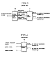
- a conventional switched reluctance motor speed control apparatus for controlling the driving circuit consists of a signal controlling stage 12 and a pulse width modulation stage 14.
- the signal controlling stage 12 For the switched reluctance motor speed control apparatus as shown in Figure 3, the signal controlling stage 12 generates a frequency control signal, a pulse width control signal, and a duty-cycle control signal.
- the frequency control signal corresponds to a rotor positional signal supplied by an A-phase position sensor (not shown), or an A-phase position signal.
- the pulse width modulation stage 14 generates a chopping signal, whose pulse width is modulated in response to three control signals output from the signal controlling stage 12, and applies it to the gate terminal of the first switching element Q1.
- the pulse width modulating stage 14 also applies the A-phase position signal to gate of the second switching element Q2.
- FIG. 4 An alternative example of a conventional speed control apparatus intended to generate a chopping signal for purpose of controlling of switched reluctance motor speed is shown in Figure 4.
- a microprocessor 16 which receives A-phase position signals from an A-phase position sensor, a speed detection sensor, and a torque sensor (not shown) and generates a chopping signal whose pulse width is modulated in frequency, pulse width and duty-cycle on the basis of the received signals and applied it to the gate of the first switching element Q1.
- the microprocessor 16 also applies the A-phase position signal to gate of the second switching element Q2.
- the first switching element Q1 is switched in response to the chopping signal during the turning-on of the switching element Q2 by the A-phase position signal, which allows the chopping of the electric current flowing in the A-phase coil 6, resulting in restriction of the increase in current and thus regulation of the current in the A-phase coil 6.
- the + A and -A poles of the stator 2 on which the A-phase coil is wound generate a magnetic force proportional to the regulated current IA by the chopping of the current waveform as described above, and rotate the rotor 4 by attracting the magnetic poles of the rotor 4 adjacent the + A- and -A poles of the stator 2, followed by the switching operations of the third to sixth switching elements Q3 to Q6 according to the respective positional signals of the B and C phases associated with the rotor 4. Then, the switching operations apply the chopped currents to the B and C phases 8, 10, which causes generation of the magnetic force proportional to the current of the chopped waveforms in the order phase A, phase B and phase C, resulting in the continuous spinning of the rotor 4.
- the switched reluctance motor speed control may be made by increasing or decreasing the electric current flowing in the phase coils 6, 8, 10 through the adjustment of the frequency, the pulse width and the duty cycle of the chopped signal in compliance with desired switched reluctance motor speed.
- a driving circuit is characterised by power supply means for applying a variable dc voltage to the switching section so as to vary the magnitude of the currents passed through the motor's stator coils and thereby control the speed of a motor being driven by the circuit.
- the power supply means composes an ac input, a rectifier and switching means for adjusting the proportion of an ac signal, applied to the ac input, that is applied to the rectifier.
- the switching means comprises an inductor, a variable resistance and a capacitor connected in series across the ac input, a triac in series with the rectifier and the ac input, and a diac connected between a terminal of the capacitor and the gate of the triac such that the diac conducts when the capacitor is charged to a predetermined level.
- a circuit according to the present invention includes a rotor position sensor for sensing the rotor position of the switched reluctance motor.
- the switching circuit comprises a plurality of switching elements and each switching element is controlled by a respective control signal solely dependent on sensed rotor position.
- the switching elements are arranged in pairs, each pair being arranged for having a stator coil of the switched reluctance motor connected in series therebetween.
- a speed control apparatus for a switched reluctance motor includes a thresholding stage 20, an ac chopping stage 30, and a rectifying stage 40.
- the thresholding stage 20 receives a commercial mains ac voltage.
- the ac chopping stage 30 controls proportion of the mains ac voltage cycle applied to the rectifying stage 40 in dependence on the thresholding stage 20.
- the rectifying stage 40 fully rectifies the chopped ac voltage to obtain a dc voltage, and then provides it to a driving circuit for the switched reluctance motor.
- the thresholding stage 20 includes a inductor L1, a resistor R1, a resistor R2 and a variable resistor VR in parallel, and a capacitor C.
- the inductor L1, the resistors R1, R2 and VR, and the capacitor are connected to form a LRC series-resonant circuit.
- the ac chopping stage 30 consists of a resistor R3, a diac DA and a triac TA.
- the diac DA generates trigger pulses for switching the triac TA to control the proportion of the ac mains cycle applied to the rectifying stage 40.
- the rectifying stage 40 consists of a diode bridge BD and a smoothing capacitor C2.
- the diode bridge BD is used to full-wave rectify the chopped ac mains, and the smoothing capacitor C2 is used to remove ripple components contained in the resulting dc voltage for application to the driving circuit 50.
- the driving circuit 50 includes six switching elements Q1, ..., Q6 for applying the dc voltage to each of phase coils 52, 54, 56, with reference to the rotor position signal of each phase input from the position sensor, and six diodes D1, ..., D6 for protecting the switching elements Q1, ..., Q6 from the back EMF created when the respective switching elements Q1, ..., Q6 are turned off.
- the impedance of the resonance frequency generating stage 20 is varied accordingly. More specifically, the capacitor C1 is charged towards the ac voltage via the three resistors R1, R2, VR and the reactance L1, and is then discharged in every cycle of the ac mains. The charging rate of the capacitor C1is varied by varying the value of the variable resistor VR. The diac DR conducts when the voltage across the capacitor C1 is outside a voltage range extending either side of 0V.
- the diac DR When the diac DR conducts, it applies a signal to the gate of the triac TR causing the triac TR to conduct. Consequently, the mains ac ( Figure 8) is chopped as shown in Figure 9. It can be seen that the triac TR remains non-conductive for the period 'a' at the start of each half-cycle, i.e. while the capacitor C1 is charging to the voltage at which the diac DR conducts. The chopped ac voltage appears across the diode bridge BD and is rectified thereby.
- the average ac voltage is given by:- where, V ave is the average ac voltage level, V 0 is the peak ac voltage, and a is chopping control angle.
- the rectified voltage from the diode bridge 40 is smoothed by the smoothing capacitor C2. Ignoring the voltage drop across the diodes of the diode bridge BD, the smoothed dc voltage is V ave.
- the dc voltage is applied to the driving circuit 50 and the switching elements Q1 - Q6 are switched in response to the rotor position signals for each phase which are applied to the appropriate gates of the switching elements Q1 - Q6, thereby applying the dc voltage to each of phase coils 52, 54, 56 in the order A, B, C.
- Coils 52, 54, 56 create magnetic force of an intensity propotional to the current flowing therethrough. This magnetic force attracts the adjacent magnetic pole of the rotor (see Figure 1) to cause the rotor to rotate. The speed of the rotor is dependent on the intensity of the magnetic force generated at coils 52, 54, 56.
Landscapes
- Engineering & Computer Science (AREA)
- Power Engineering (AREA)
- Control Of Electric Motors In General (AREA)
Description
- The present invention relates to a driving circuit for a switched reluctance motor, comprising a switching circuit arranged to selectively pass currents through the stator coils of a switched reluctance motor in dependence on the position of the rotor of the motor being driven.
- Referring to Figure 1, a switched reluctance motor (switched reluctance motor) has a
stator 2 and arotor 4. Thestator 2 has A-, B- and C-phase coils - Referring to Figure 2, a driving circuit for such a switched reluctance motor comprises a smoothing capacitor C for providing a dc voltage, first to sixth switching elements Q1, ...,Q6 for applying electric current to the
phase coils - Referring to Figure 3, a conventional switched reluctance motor speed control apparatus for controlling the driving circuit consists of a
signal controlling stage 12 and a pulsewidth modulation stage 14. - For the switched reluctance motor speed control apparatus as shown in Figure 3, the
signal controlling stage 12 generates a frequency control signal, a pulse width control signal, and a duty-cycle control signal. The frequency control signal corresponds to a rotor positional signal supplied by an A-phase position sensor (not shown), or an A-phase position signal. The pulsewidth modulation stage 14 generates a chopping signal, whose pulse width is modulated in response to three control signals output from thesignal controlling stage 12, and applies it to the gate terminal of the first switching element Q1. The pulsewidth modulating stage 14 also applies the A-phase position signal to gate of the second switching element Q2. - An alternative example of a conventional speed control apparatus intended to generate a chopping signal for purpose of controlling of switched reluctance motor speed is shown in Figure 4. Further prior art uses a
microprocessor 16 which receives A-phase position signals from an A-phase position sensor, a speed detection sensor, and a torque sensor (not shown) and generates a chopping signal whose pulse width is modulated in frequency, pulse width and duty-cycle on the basis of the received signals and applied it to the gate of the first switching element Q1. Themicroprocessor 16 also applies the A-phase position signal to gate of the second switching element Q2. - If the chopping signal from the pulse
width modulation stage 14 and the A-phase position signal are applied respectively to the first and second switching elements Q1, Q2, these elements Q1, Q2 are switched in response thereto, thereby supplying power to theA-phase coil 6. At this time, the voltage across and the current flowing in theA-phase coil 6 are as shown in Figure 5. - The first switching element Q1 is switched in response to the chopping signal during the turning-on of the switching element Q2 by the A-phase position signal, which allows the chopping of the electric current flowing in the
A-phase coil 6, resulting in restriction of the increase in current and thus regulation of the current in theA-phase coil 6. - The + A and -A poles of the
stator 2 on which the A-phase coil is wound generate a magnetic force proportional to the regulated current IA by the chopping of the current waveform as described above, and rotate therotor 4 by attracting the magnetic poles of therotor 4 adjacent the + A- and -A poles of thestator 2, followed by the switching operations of the third to sixth switching elements Q3 to Q6 according to the respective positional signals of the B and C phases associated with therotor 4. Then, the switching operations apply the chopped currents to the B andC phases rotor 4. - Due to the fact that the speed of the
rotor 4 depends upon the intensity of the generated magnetic force, the switched reluctance motor speed control may be made by increasing or decreasing the electric current flowing in thephase coils - However, if the switched reluctance motor is rotated at high speed (e.g. 3000 rpm), the periods of the rotor positional signals, which are generated from the position sensors for each phase, become extremely short. This causes the pulse
width modulation stage 14 to generate a chopping signal whose frequency exceeds the switching speeds of the first, third and fifth switching elements Q1, Q3, Q5, so that switching cannot promptly be performed in response to the chopping signal. Thus, a problem arises in that inaccurate control of the current in each phase coil of thestator 2 results in worse control of the motor speed. - It is an aim of the present invention to overcome the afore-mentioned problem.
- A driving circuit according to the present invention is characterised by power supply means for applying a variable dc voltage to the switching section so as to vary the magnitude of the currents passed through the motor's stator coils and thereby control the speed of a motor being driven by the circuit.
- Preferably, the power supply means composes an ac input, a rectifier and switching means for adjusting the proportion of an ac signal, applied to the ac input, that is applied to the rectifier.
- Preferably, the switching means comprises an inductor, a variable resistance and a capacitor connected in series across the ac input, a triac in series with the rectifier and the ac input, and a diac connected between a terminal of the capacitor and the gate of the triac such that the diac conducts when the capacitor is charged to a predetermined level.
- Preferably, a circuit according to the present invention includes a rotor position sensor for sensing the rotor position of the switched reluctance motor. More preferably, the switching circuit comprises a plurality of switching elements and each switching element is controlled by a respective control signal solely dependent on sensed rotor position. Still more preferably, the switching elements are arranged in pairs, each pair being arranged for having a stator coil of the switched reluctance motor connected in series therebetween.
- An embodiment of the present invention will now be described, by way of example, with reference to Figures 6 to 10 of the accompanying drawings, in which:
- Figure 1 illustrates the construction of a conventional switched reluctance motor;
- Figure 2 is a circuit diagram of a driving circuit for the conventional switched reluctance motor of Figure 1;
- Figure 3 is a block diagram of a conventional switched reluctance motor speed control apparatus;
- Figure 4 is a block diagram of another conventional switched reluctance motor speed control apparatus;
- Figure 5 illustrates the controlled voltage and current waveforms for a stator coil;
- Figure 6 is a block diagram of a switched reluctance motor speed control apparatus in accordance with the present invention;
- Figure 7 is a circuit diagram of a driving circuit according to the present invention;
- Figure 8 illustrates the voltage waveform of a mains supply;
- Figure 9 illustrates the waveform of the phase-controlled ac voltage produced by the ac chopping stage of Figure 7; and
- Figure 10 illustrates the current and voltage waveforms for a stator coil, controlled by speed control apparatus according to the present invention.
-
- Referring to Figure 6, a speed control apparatus for a switched reluctance motor includes a
thresholding stage 20, anac chopping stage 30, and a rectifyingstage 40. - The
thresholding stage 20 receives a commercial mains ac voltage. Theac chopping stage 30 controls proportion of the mains ac voltage cycle applied to the rectifyingstage 40 in dependence on thethresholding stage 20. - The rectifying
stage 40 fully rectifies the chopped ac voltage to obtain a dc voltage, and then provides it to a driving circuit for the switched reluctance motor. - Referring to Figure 7. the
thresholding stage 20 includes a inductor L1, a resistor R1, a resistor R2 and a variable resistor VR in parallel, and a capacitor C. The inductor L1, the resistors R1, R2 and VR, and the capacitor are connected to form a LRC series-resonant circuit. - The ac chopping
stage 30 consists of a resistor R3, a diac DA and a triac TA. The diac DA generates trigger pulses for switching the triac TA to control the proportion of the ac mains cycle applied to the rectifyingstage 40. - The rectifying
stage 40 consists of a diode bridge BD and a smoothing capacitor C2. The diode bridge BD is used to full-wave rectify the chopped ac mains, and the smoothing capacitor C2 is used to remove ripple components contained in the resulting dc voltage for application to thedriving circuit 50. - The
driving circuit 50 includes six switching elements Q1, ..., Q6 for applying the dc voltage to each ofphase coils - The operation of the circuit shown in Figure 7 will now be described with reference to Figures 6 to 10.
- When a user adjusts the variable resistor VR of the
thresholding stage 20 to obtain a desired motor speed, the impedance of the resonancefrequency generating stage 20 is varied accordingly. More specifically, the capacitor C1 is charged towards the ac voltage via the three resistors R1, R2, VR and the reactance L1, and is then discharged in every cycle of the ac mains. The charging rate of the capacitor C1is varied by varying the value of the variable resistor VR. The diac DR conducts when the voltage across the capacitor C1 is outside a voltage range extending either side of 0V. - When the diac DR conducts, it applies a signal to the gate of the triac TR causing the triac TR to conduct. Consequently, the mains ac (Figure 8) is chopped as shown in Figure 9. It can be seen that the triac TR remains non-conductive for the period 'a' at the start of each half-cycle, i.e. while the capacitor C1 is charging to the voltage at which the diac DR conducts. The chopped ac voltage appears across the diode bridge BD and is rectified thereby.
- As a result of the chopping, the average value of ac voltage applied to the diode bridge BD is reduced. The average ac voltage is given by:-where, Vave is the average ac voltage level, V0 is the peak ac voltage, and a is chopping control angle.

- The rectified voltage from the
diode bridge 40 is smoothed by the smoothing capacitor C2. Ignoring the voltage drop across the diodes of the diode bridge BD, the smoothed dc voltage is Vave. - The dc voltage is applied to the
driving circuit 50 and the switching elements Q1 - Q6 are switched in response to the rotor position signals for each phase which are applied to the appropriate gates of the switching elements Q1 - Q6, thereby applying the dc voltage to each ofphase coils - The waveforms of the voltages and currents applied to each coil of each phase are shown in Figure 10.
Coils coils
Claims (5)
- A driving circuit for a switched reluctance motor, comprising a switching circuit (50) arranged to selectively pass currents through the stator coils of a switched reluctance motor in dependence on the position of the rotor of the motor being driven,
characterised by power supply means (20, 30, 40) for applying a variable dc voltage to the switching section so as to vary the magnitude of said currents and thereby control the speed of a motor being driven by the circuit. - A circuit according to claim 1, wherein the power supply means comprises an ac input, a rectifier (40) and switching means (20, 30) for adjusting the proportion of an ac signal, applied to the ac input, that is applied to the rectifier.
- A circuit according to claim 2, wherein the switching means comprises an inductor (L1), a variable resistance (R1, R2, VR) and a capacitor (C1) connected in series across the ac input, a triac in series with the rectifier and the ac input, and a diac connected between a terminal of the capacitor and the gate of the triac such that the diac conducts when the capacitor is charged to a predetermined level.
- A circuit according to any preceding claim, including a rotor position sensor for sensing the rotor position of the switched reluctance motor, wherein the switching circuit comprises a plurality of switching elements (Q1, ..., Q6) and each switching element is controlled by a respective control signal solely dependent on sensed rotor position.
- A circuit according to claim 4, wherein the switching elements are arranged in pairs, each pair being arranged for having a stator coil of the switched reluctance motor connected in series therebetween.
Applications Claiming Priority (2)
| Application Number | Priority Date | Filing Date | Title |
|---|---|---|---|
| KR1019960051767A KR100210083B1 (en) | 1996-11-04 | 1996-11-04 | Speed control apparatus of a switched reluctance motor |
| KR9651767 | 1996-11-04 |
Publications (3)
| Publication Number | Publication Date |
|---|---|
| EP0840438A2 EP0840438A2 (en) | 1998-05-06 |
| EP0840438A3 EP0840438A3 (en) | 1998-10-14 |
| EP0840438B1 true EP0840438B1 (en) | 2004-11-17 |
Family
ID=19480670
Family Applications (1)
| Application Number | Title | Priority Date | Filing Date |
|---|---|---|---|
| EP97307568A Expired - Lifetime EP0840438B1 (en) | 1996-11-04 | 1997-09-26 | Switched reluctance motor driving circuit |
Country Status (6)
| Country | Link |
|---|---|
| US (1) | US5821723A (en) |
| EP (1) | EP0840438B1 (en) |
| JP (1) | JPH10146082A (en) |
| KR (1) | KR100210083B1 (en) |
| CN (1) | CN1055809C (en) |
| DE (1) | DE69731594T2 (en) |
Families Citing this family (13)
| Publication number | Priority date | Publication date | Assignee | Title |
|---|---|---|---|---|
| JPH11103594A (en) * | 1997-09-29 | 1999-04-13 | Meidensha Corp | Drive circuit of switched reluctance motor |
| US6566839B2 (en) * | 2001-06-28 | 2003-05-20 | Pelco | Switched capacitor motor driver |
| US6873130B2 (en) * | 2001-07-12 | 2005-03-29 | Delaware Capital Formation | Method and apparatus for maintaining force of a variable reluctance motor |
| DE102005051646A1 (en) * | 2005-10-26 | 2007-05-10 | Otto Bock Healthcare Ip Gmbh & Co. Kg | Procedure for checking the setting of a prosthetic knee joint |
| CN101317326B (en) * | 2006-10-25 | 2011-08-03 | Lg电子株式会社 | Apparatus and method for driving two-phase SRM electric motor |
| WO2008050919A1 (en) * | 2006-10-25 | 2008-05-02 | Lg Electronics Inc. | Apparatus and method for driving 2-phase srm |
| WO2009099342A2 (en) * | 2008-02-08 | 2009-08-13 | Restech Limited | Electromagnetic field energy recycling |
| US8525450B2 (en) * | 2010-03-29 | 2013-09-03 | Regal Beloit America, Inc. | Power factor correction drive circuit topologies and control for switched reluctance machines |
| CN102931901B (en) * | 2012-10-31 | 2015-10-28 | 奇瑞汽车股份有限公司 | A kind of switched reluctance machines power-generating control system and control method thereof |
| US9413163B2 (en) | 2014-06-19 | 2016-08-09 | Texas Instruments Incorporated | Motor fault detector |
| KR101677598B1 (en) | 2014-12-11 | 2016-11-21 | 한국산업기술대학교산학협력단 | Controller for driving a switched reluctance motor having low noise and the method thereof |
| EP3101805B1 (en) * | 2015-06-01 | 2019-04-03 | Aros Electronics AB | Dc bus ripple reduction |
| US10516322B2 (en) * | 2016-05-19 | 2019-12-24 | Arm Ltd. | Method and apparatus for maintenance of electric motor |
Family Cites Families (11)
| Publication number | Priority date | Publication date | Assignee | Title |
|---|---|---|---|---|
| US3663877A (en) * | 1970-04-02 | 1972-05-16 | Ampex | Brushless dc motor including tachometer commutation circuit |
| US3643140A (en) * | 1970-08-07 | 1972-02-15 | Armec Corp | Dc energized timing motor utilizing a resonant member to maintain constant speed |
| US4321662A (en) * | 1979-06-29 | 1982-03-23 | Nippon Gakki Seizo Kabushiki Kaisha | Power supply circuit for electrical apparatus |
| US4297626A (en) * | 1980-02-07 | 1981-10-27 | David Chiang | Method of determining operating currents for stepping motor |
| US4584512A (en) * | 1980-02-27 | 1986-04-22 | Pritchard Eric K | Microstepping drives with waveform tuning and microprocessor control |
| US4353016A (en) * | 1981-04-22 | 1982-10-05 | Minnesota Mining And Manufacturing Company | Linear motor control system for brushless DC motor |
| US4511834A (en) * | 1982-12-23 | 1985-04-16 | Borg-Warner Corporation | Control and stabilizing system for damperless synchronous motor |
| GB2157089A (en) * | 1984-03-26 | 1985-10-16 | Ching Chuen Chan | Single-phase reluctance motor |
| US4584506A (en) * | 1984-11-23 | 1986-04-22 | Polestar Magnetronics Inc. | Reluctance motor with electronically controlled stator windings |
| US5559685A (en) * | 1994-10-12 | 1996-09-24 | Electronic Power Conditioning, Inc. | Voltage clamped parallel resonant converter with controllable duty cycle |
| US5689164A (en) * | 1995-12-08 | 1997-11-18 | Kabushiki Kaisha Toyoda Jidoshokki Seisakusho | Resonant power electronic control of switched reluctance motor |
-
1996
- 1996-11-04 KR KR1019960051767A patent/KR100210083B1/en not_active IP Right Cessation
-
1997
- 1997-08-12 US US08/912,990 patent/US5821723A/en not_active Expired - Fee Related
- 1997-09-01 CN CN97117555A patent/CN1055809C/en not_active Expired - Fee Related
- 1997-09-17 JP JP9252510A patent/JPH10146082A/en active Pending
- 1997-09-26 EP EP97307568A patent/EP0840438B1/en not_active Expired - Lifetime
- 1997-09-26 DE DE69731594T patent/DE69731594T2/en not_active Expired - Fee Related
Also Published As
| Publication number | Publication date |
|---|---|
| CN1055809C (en) | 2000-08-23 |
| JPH10146082A (en) | 1998-05-29 |
| DE69731594D1 (en) | 2004-12-23 |
| KR19980033924A (en) | 1998-08-05 |
| CN1181657A (en) | 1998-05-13 |
| EP0840438A3 (en) | 1998-10-14 |
| DE69731594T2 (en) | 2005-03-31 |
| EP0840438A2 (en) | 1998-05-06 |
| US5821723A (en) | 1998-10-13 |
| KR100210083B1 (en) | 1999-07-15 |
Similar Documents
| Publication | Publication Date | Title |
|---|---|---|
| EP0840438B1 (en) | Switched reluctance motor driving circuit | |
| US5825597A (en) | System and method for detection and control of circulating currents in a motor | |
| EP0881760B1 (en) | Single phase motor drive | |
| JP3634443B2 (en) | Inductive load control circuit | |
| US6051942A (en) | Method and apparatus for controlling a switched reluctance machine | |
| CA1228640A (en) | Current control method and circuit for electronically- commutated motors | |
| US20010048278A1 (en) | Cross coupled motor gate drive | |
| GB2314703A (en) | Driving circuit for a switched reluctance motor | |
| CA2108343A1 (en) | Electronic power regulator for an automotive alternator | |
| JPH0124031B2 (en) | ||
| KR20010014903A (en) | Control of line harmonics | |
| JP4226224B2 (en) | Inverter device | |
| US5220258A (en) | Drive circuit for a brushless direct-current motor | |
| US5598073A (en) | Drive circuit for a brushless direct-current motor | |
| EP0769843A1 (en) | A method and apparatus for controlling static electronic components for phase switching in a three-phase brushless electric motor | |
| GB2323725A (en) | Control circuit for a switched reluctance motor | |
| JP3734583B2 (en) | Power supply | |
| US4864212A (en) | Energy economizing AC power system | |
| JPH07312898A (en) | Three-phase electric inverter of variable-speed motor and its driving method | |
| US5990655A (en) | Method of operating an inverter for powering an induction motor | |
| Natarajan et al. | Universal Motor with On-Off Controller for Washing Machine Application | |
| KR100239508B1 (en) | Speed control apparatus of motor and method thereof | |
| EP0872012A1 (en) | A device for control of the speed of a series motor | |
| JP2639985B2 (en) | Control method of single-phase induction motor | |
| JP4558862B2 (en) | Drive system and method for inverter system |
Legal Events
| Date | Code | Title | Description |
|---|---|---|---|
| PUAI | Public reference made under article 153(3) epc to a published international application that has entered the european phase |
Free format text: ORIGINAL CODE: 0009012 |
|
| AK | Designated contracting states |
Kind code of ref document: A2 Designated state(s): DE FR GB |
|
| AX | Request for extension of the european patent |
Free format text: AL;LT;LV;RO;SI |
|
| PUAL | Search report despatched |
Free format text: ORIGINAL CODE: 0009013 |
|
| AK | Designated contracting states |
Kind code of ref document: A3 Designated state(s): AT BE CH DE DK ES FI FR GB GR IE IT LI LU MC NL PT SE |
|
| AX | Request for extension of the european patent |
Free format text: AL;LT;LV;RO;SI |
|
| 17P | Request for examination filed |
Effective date: 19990311 |
|
| AKX | Designation fees paid |
Free format text: DE FR GB |
|
| 17Q | First examination report despatched |
Effective date: 20030401 |
|
| GRAP | Despatch of communication of intention to grant a patent |
Free format text: ORIGINAL CODE: EPIDOSNIGR1 |
|
| GRAS | Grant fee paid |
Free format text: ORIGINAL CODE: EPIDOSNIGR3 |
|
| GRAA | (expected) grant |
Free format text: ORIGINAL CODE: 0009210 |
|
| RAP1 | Party data changed (applicant data changed or rights of an application transferred) |
Owner name: SAMSUNG ELECTRONICS CO., LTD. |
|
| AK | Designated contracting states |
Kind code of ref document: B1 Designated state(s): DE FR GB |
|
| REG | Reference to a national code |
Ref country code: GB Ref legal event code: FG4D |
|
| REF | Corresponds to: |
Ref document number: 69731594 Country of ref document: DE Date of ref document: 20041223 Kind code of ref document: P |
|
| PLBE | No opposition filed within time limit |
Free format text: ORIGINAL CODE: 0009261 |
|
| STAA | Information on the status of an ep patent application or granted ep patent |
Free format text: STATUS: NO OPPOSITION FILED WITHIN TIME LIMIT |
|
| ET | Fr: translation filed | ||
| 26N | No opposition filed |
Effective date: 20050818 |
|
| PGFP | Annual fee paid to national office [announced via postgrant information from national office to epo] |
Ref country code: DE Payment date: 20070920 Year of fee payment: 11 |
|
| PGFP | Annual fee paid to national office [announced via postgrant information from national office to epo] |
Ref country code: GB Payment date: 20070926 Year of fee payment: 11 |
|
| PGFP | Annual fee paid to national office [announced via postgrant information from national office to epo] |
Ref country code: FR Payment date: 20070914 Year of fee payment: 11 |
|
| GBPC | Gb: european patent ceased through non-payment of renewal fee |
Effective date: 20080926 |
|
| REG | Reference to a national code |
Ref country code: FR Ref legal event code: ST Effective date: 20090529 |
|
| PG25 | Lapsed in a contracting state [announced via postgrant information from national office to epo] |
Ref country code: DE Free format text: LAPSE BECAUSE OF NON-PAYMENT OF DUE FEES Effective date: 20090401 |
|
| PG25 | Lapsed in a contracting state [announced via postgrant information from national office to epo] |
Ref country code: FR Free format text: LAPSE BECAUSE OF NON-PAYMENT OF DUE FEES Effective date: 20080930 |
|
| PG25 | Lapsed in a contracting state [announced via postgrant information from national office to epo] |
Ref country code: GB Free format text: LAPSE BECAUSE OF NON-PAYMENT OF DUE FEES Effective date: 20080926 |