EP0838840B1 - Pulsed plate plasma implantation method and apparatus - Google Patents
Pulsed plate plasma implantation method and apparatus Download PDFInfo
- Publication number
- EP0838840B1 EP0838840B1 EP97307902A EP97307902A EP0838840B1 EP 0838840 B1 EP0838840 B1 EP 0838840B1 EP 97307902 A EP97307902 A EP 97307902A EP 97307902 A EP97307902 A EP 97307902A EP 0838840 B1 EP0838840 B1 EP 0838840B1
- Authority
- EP
- European Patent Office
- Prior art keywords
- treatment
- workpiece support
- treatment chamber
- workpieces
- chamber
- Prior art date
- Legal status (The legal status is an assumption and is not a legal conclusion. Google has not performed a legal analysis and makes no representation as to the accuracy of the status listed.)
- Expired - Lifetime
Links
- 238000000034 method Methods 0.000 title claims description 24
- 238000002513 implantation Methods 0.000 title description 22
- 150000002500 ions Chemical class 0.000 claims description 36
- 239000000463 material Substances 0.000 claims description 8
- 239000002245 particle Substances 0.000 claims description 8
- 229910052757 nitrogen Inorganic materials 0.000 claims description 6
- 230000005855 radiation Effects 0.000 claims description 5
- 239000011810 insulating material Substances 0.000 claims description 2
- 239000004020 conductor Substances 0.000 claims 1
- 230000036470 plasma concentration Effects 0.000 claims 1
- 239000007789 gas Substances 0.000 description 24
- 235000012431 wafers Nutrition 0.000 description 24
- 238000005468 ion implantation Methods 0.000 description 13
- XUIMIQQOPSSXEZ-UHFFFAOYSA-N Silicon Chemical compound [Si] XUIMIQQOPSSXEZ-UHFFFAOYSA-N 0.000 description 9
- 229910052710 silicon Inorganic materials 0.000 description 9
- 239000010703 silicon Substances 0.000 description 9
- IJGRMHOSHXDMSA-UHFFFAOYSA-N Atomic nitrogen Chemical compound N#N IJGRMHOSHXDMSA-UHFFFAOYSA-N 0.000 description 6
- 238000010884 ion-beam technique Methods 0.000 description 5
- ZOXJGFHDIHLPTG-UHFFFAOYSA-N Boron Chemical compound [B] ZOXJGFHDIHLPTG-UHFFFAOYSA-N 0.000 description 4
- 229910052796 boron Inorganic materials 0.000 description 4
- 239000007787 solid Substances 0.000 description 4
- XAGFODPZIPBFFR-UHFFFAOYSA-N aluminium Chemical compound [Al] XAGFODPZIPBFFR-UHFFFAOYSA-N 0.000 description 3
- 229910052782 aluminium Inorganic materials 0.000 description 3
- 238000011109 contamination Methods 0.000 description 3
- 230000005684 electric field Effects 0.000 description 3
- WTEOIRVLGSZEPR-UHFFFAOYSA-N boron trifluoride Chemical compound FB(F)F WTEOIRVLGSZEPR-UHFFFAOYSA-N 0.000 description 2
- 238000006243 chemical reaction Methods 0.000 description 2
- 229910001873 dinitrogen Inorganic materials 0.000 description 2
- 239000007943 implant Substances 0.000 description 2
- 230000003993 interaction Effects 0.000 description 2
- 238000010849 ion bombardment Methods 0.000 description 2
- 238000004519 manufacturing process Methods 0.000 description 2
- 239000010453 quartz Substances 0.000 description 2
- VYPSYNLAJGMNEJ-UHFFFAOYSA-N silicon dioxide Inorganic materials O=[Si]=O VYPSYNLAJGMNEJ-UHFFFAOYSA-N 0.000 description 2
- 239000000758 substrate Substances 0.000 description 2
- 229910021417 amorphous silicon Inorganic materials 0.000 description 1
- 238000004380 ashing Methods 0.000 description 1
- 239000011248 coating agent Substances 0.000 description 1
- 238000000576 coating method Methods 0.000 description 1
- 230000003247 decreasing effect Effects 0.000 description 1
- 238000009792 diffusion process Methods 0.000 description 1
- 239000002019 doping agent Substances 0.000 description 1
- 230000008030 elimination Effects 0.000 description 1
- 238000003379 elimination reaction Methods 0.000 description 1
- 239000011521 glass Substances 0.000 description 1
- 230000003116 impacting effect Effects 0.000 description 1
- 239000012212 insulator Substances 0.000 description 1
- 230000005865 ionizing radiation Effects 0.000 description 1
- 238000012423 maintenance Methods 0.000 description 1
- 230000007935 neutral effect Effects 0.000 description 1
- 238000002161 passivation Methods 0.000 description 1
- 229920002120 photoresistant polymer Polymers 0.000 description 1
- 238000001020 plasma etching Methods 0.000 description 1
- 229910021420 polycrystalline silicon Inorganic materials 0.000 description 1
- 229920005591 polysilicon Polymers 0.000 description 1
- 230000000750 progressive effect Effects 0.000 description 1
- 238000004151 rapid thermal annealing Methods 0.000 description 1
- 238000005215 recombination Methods 0.000 description 1
- 230000006798 recombination Effects 0.000 description 1
- 230000001105 regulatory effect Effects 0.000 description 1
- 230000003252 repetitive effect Effects 0.000 description 1
- 239000000523 sample Substances 0.000 description 1
- 239000004065 semiconductor Substances 0.000 description 1
- 238000004544 sputter deposition Methods 0.000 description 1
Images

Classifications
-
- H—ELECTRICITY
- H01—ELECTRIC ELEMENTS
- H01J—ELECTRIC DISCHARGE TUBES OR DISCHARGE LAMPS
- H01J37/00—Discharge tubes with provision for introducing objects or material to be exposed to the discharge, e.g. for the purpose of examination or processing thereof
- H01J37/32—Gas-filled discharge tubes
- H01J37/32009—Arrangements for generation of plasma specially adapted for examination or treatment of objects, e.g. plasma sources
- H01J37/32412—Plasma immersion ion implantation
-
- C—CHEMISTRY; METALLURGY
- C23—COATING METALLIC MATERIAL; COATING MATERIAL WITH METALLIC MATERIAL; CHEMICAL SURFACE TREATMENT; DIFFUSION TREATMENT OF METALLIC MATERIAL; COATING BY VACUUM EVAPORATION, BY SPUTTERING, BY ION IMPLANTATION OR BY CHEMICAL VAPOUR DEPOSITION, IN GENERAL; INHIBITING CORROSION OF METALLIC MATERIAL OR INCRUSTATION IN GENERAL
- C23C—COATING METALLIC MATERIAL; COATING MATERIAL WITH METALLIC MATERIAL; SURFACE TREATMENT OF METALLIC MATERIAL BY DIFFUSION INTO THE SURFACE, BY CHEMICAL CONVERSION OR SUBSTITUTION; COATING BY VACUUM EVAPORATION, BY SPUTTERING, BY ION IMPLANTATION OR BY CHEMICAL VAPOUR DEPOSITION, IN GENERAL
- C23C14/00—Coating by vacuum evaporation, by sputtering or by ion implantation of the coating forming material
- C23C14/22—Coating by vacuum evaporation, by sputtering or by ion implantation of the coating forming material characterised by the process of coating
- C23C14/48—Ion implantation
Definitions
- the present invention concerns a workpiece treatment system that immerses a workpiece to be treated into a plasma of particles that are accelerated to impact the workpiece.
- One such system immerses one or more workpieces into a plasma containing positively charged ions that are subsequently accelerated toward the surface of silicon wafers to dope the wafers with a controlled concentration of the ions.
- ion implantation systems employ an ion source that includes a source chamber spaced from an implantation chamber where one or more workpieces are treated by ions from the source.
- An exit opening in the source chamber allows ions to exit the source so they can be shaped, analyzed, and accelerated to form an ion beam.
- the ion beam is directed along an evacuated beam path to the ion implantation chamber where the ion beam strikes one or more workpieces, typically circular wafers that have been placed within the implantation chamber.
- the energy of the ion beam is sufficient to cause ions which strike the wafers to penetrate those wafers in the implantation chamber.
- the wafers are silicon wafers and the ions are used to "dope" the wafers to create a semiconductor material.
- Selective implantation with the use of masks and passivation layers allows an integrated circuit to be fabricated with such a prior art implanter.
- United States Patent 4,764,394 to Conrad entitled “Method and Apparatus for Plasma-Source Ion Implantation” discloses an ion implantation system for treating a target by means of ionic bombardment. Ion implantation into surfaces of a three dimensional target is achieved by forming an ionized plasma about the target within an enclosing chamber. Once the plasma is set up in a region surrounding the target, ions from the plasma are driven into the target object from all sides without need to manipulate the target. This implantation is accomplished by application of repetitive pulses of high voltage, typically 20. kilovolts or higher, that cause the ions to be driven into exposed surfaces of the target.
- a technique discussed in the '394 patent for setting up the plasma is to introduce a neutral gas into the region of the target and then ionize the gas with ionizing radiation.
- the system disclosed in the '394 patent to Conrad sets up, by using a separate ion source, an ion plasma in a region surrounding a workpiece and then selectively pulses with negative voltage an electrode that supports the workpiece to attract the positive ions in the plasma to the workpiece.
- Structure and method constructed in accordance with the present invention accomplish both plasma creation and workpiece treatment with one sequence of energization pulses.
- US-A-5 354 381 and EP-A-0 596 496 disclose implantation apparatuses wherein the wafer is mounted on an electrode and negative pulses are applied to the electrode to create a plasma. The ions produced are then accelerated toward and implanted in the wafer.
- Embodiments of the present invention concern treatment of a workpiece by particle bombardment of the workpiece.
- An implantation chamber is provided that has a chamber interior.
- a conductive workpiece support acts as one electrode and positions one or more workpieces within the chamber interior.
- the chamber has a conductive wall portion that bounds the chamber interior.
- One or more workpieces are inserted into the implantation chamber and placed onto the conductive support so that treatment surfaces of the one or more workpieces face an interior region of the implantation chamber.
- a workpiece treatment material in the form of neutrally charged gas molecules is injected by an injector into the implantation chamber so that the gas occupies a region of the implantation chamber in close proximity to the one or more workpieces supported by the conductive support.
- a biasing voltage is applied between the conductive workpiece support, which forms one electrode, and the injector, which forms a second electrode.
- the biasing voltage is most preferably a sequence of electric pulses for relatively biasing the first and second electrodes to both ionize the gas molecules injected into the chamber and accelerate charged particles resulting from this ionization toward the treatment surfaces of the one or more workpieces.
- Flat panel displays are fabricated from a substrate of glass or the like having a coating of either a polysilicon or amorphous silicon applied to one surface. The coated substrate is inserted into the ion implantation chamber and treated by ion bombardment.
- Embodiments of the present invention have certain advantages over prior art ion implanters having an ion source spaced from an implantation station by relatively lengthy evacuated ion beam paths.
- the cost of manufacturing an ion implanter constructed in accordance with the invention should be less due to elimination of the plasma sources and the power supplies for such a source.
- the size of the process chamber can be reduced since the gap between the electrodes that create the plasma within the chamber can be made relatively. small.
- the cost of operation of such an implanter may be reduced since the size of the system, the power consumption and the maintenance are simpler to perform.
- the contamination of the implanter may be reduced as the plasma is confined between the two plates.
- the ability to treat large cross section workpieces such as flat panel displays is enhanced since only the size of electrodes need be increased to increase the size of the workpiece that can be treated. Uniformity of implantation is also very good and variations of about or less than 1% can be achieved.
- Use of the disclosed techniques for setting up a plasma is not limited to ion implantation.
- the disclosed techniques can also be used for plasma etching or ashing. If the polarity of the pulsing applied to the first and second electrodes is reversed, the workpiece can be treated with electrons, which in certain instances such as treatment of photoresists can be useful. In general, positive or negative voltages can be applied to either one of the first and second electrodes and the other electrode can be kept at a reference, typically ground potential.
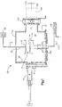
- FIG 1 is an overview schematic of an ion implantation system 10 that includes a process chamber 12 into which generally planar workpieces 14 are inserted for ion treatment of those workpieces.
- the system depicted in Figure 1 includes a loadlock 20 for inserting individual wafers into the process chamber 12 one at a time.
- the use of a loadlock allows the process chamber 12 to be maintained at a reduced pressure (in relation to atmospheric pressure) as workpieces are placed into and withdrawn from the chamber 12 by means of a valve 21 that is opened and closed as workpieces are inserted into and retrieved from the process chamber 12.
- the process chamber 12 depicted in Figure 1 has inner walls 22 that define a chamber interior 24 into which a workpiece 14 has been inserted.
- the workpiece 14 is placed onto a generally planar conductive platen or support 30.
- the platen 30 may have any suitable dimensions depending, for example, on the size of the workpiece to be supported by the platen 30.
- a gas delivery manifold 32 Spaced above the workpiece platen is a gas delivery manifold 32 that injects an ionizable gas to a region 34 between the manifold and the workpiece 14.
- This region 34 above the workpiece is a region wherein an ion plasma is created during operation of the implantation system 10.
- Gas molecules not ionized and implanted are withdrawn from the chamber through exit openings 35.
- the exit openings 35 are formed beneath the platen 30.
- a gas supply 36 outside the chamber delivers an ionizable gas through an inlet 37 passing through a chamber wall into the manifold which defines multiple diverging passageways leading from the inlet 37 to an array of.openings 40 ( Figures 2A and 2B) facing the workpiece 14.
- Good treatment uniformity is obtained by keeping the gas density in the region 34 between the manifold and the workpiece 14 as uniform as possible.
- a preferred manifold 32 is generally circular in plan and includes an array of openings 40 to maintain the gas concentration as uniform as possible around the outer perimeter of the manifold.
- the workpieces 14 are placed onto the platen 30 spaced inwardly from the edge of the generally circular platen 30 to avoid potentially nonuniform regions of the plasma. Uniform implantation may also be ensured by suitable design of the shape of the edges of the platen 30 as the first electrode and the manifold 32 as the second electrode to control the electrical field strength at the edges of the electrodes.
- the gas molecules are ionized (stripped of one or more electrons) and the positively charged atoms are accelerated toward the workpiece by a sequence of negative voltage pulses that are applied to the conductive platen 30 ( Figure 2A) while the manifold 32 is maintained at a ground potential.
- the polarity of voltages applied to the platen 30 and manifold 32 could be reversed, resulting in electrons accelerated to impact the workpiece.
- a single workpiece is shown supported on the platen 30, but multiple workpieces could also be simultaneously implanted.
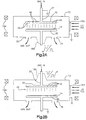
- Figures 2A and 2B illustrate four different relative biasing arrangements used for creating a concentration of workpiece treatment material in the region 34 above the workpiece 14.
- the manifold 32 and chamber walls are grounded.
- negative voltage pulses N applied to the conductive support platen 30 cause ions to be created by the relatively high electric field in the region 34 and accelerated toward the platen.
- the support platen 30 is grounded and the voltage pulses are applied to the manifold 32.
- positive voltage pulses P accelerate positively charged ions toward the workpiece 14.
- a modulator circuit 100 located outside the chamber 12 applies voltage pulses across the platen 30 as one electrode and the manifold 32 as another electrode to relatively bias the conductive platen 30 and the conductive manifold 32. Any one of a number of commercially acceptable voltage sources are suitable for supplying voltage pulses.
- a preferred modulator circuit 100 includes a voltage source controlled by relatively high power solid state switches that provides a sequence of pulses 112 that both ionize the gas molecules injected into the chamber and accelerate the ionized gas molecules toward implantation surfaces of the one or more workpieces 14.
- the repetition rate and pulse duration of the pulses 112 are chosen to assure that a glow discharge is developed and a plasma is formed and maintained in the region 34 by the pulses applied to the two electrodes 30, 32.
- the plasma density can decay in a time on the order of milliseconds due to recombination and diffusion after the ionization pulse is removed.
- a pulse rate of thousands per second or greater is necessary. However, at lower pulse rates, the ionization and implantation are still occurring during each pulse but provide a lower implantation rate.
- the platen 30 and the manifold 32 for one embodiment are formed of aluminum coated by silicon. Lining at least a portion of the chamber walls 22 and/or the non-working area of the platen 30 with a suitable insulating material, such as quartz for example, also helps to reduce contamination as well as power consumption.
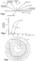
- Figure 3 illustrates possible reactions occurring at a treatment surface 120 of a workpiece 14 as ions 130 from the ion plasma region 34 strike the surface 120.
- the possible ion-surface interactions illustrated in Figure 3 give rise to both inelastic (production of photons, X-rays, secondary electrons, as well as ion implantation) and elastic (sputtering and reflected particles) reactions.
- An incident ion 130 can be trapped in a solid lattice of the workpiece 14 and this is ion implantation.
- the ion energy is mainly determined by the sheath voltage of the plasma, which in turn is dictated by the pulse voltage supplied by the modulator 100.
- the trapping probability is also affected by gas pressure, since ions may lose part of their energy due to collisions with gas molecules before they reach the surface 120.
- a vacuum pump 140 maintains the chamber interior at a reduced pressure that is regulated by a valve 142 inserted between the chamber 12 and the pump 140.
- the same pump 140 can alternatively be coupled to the gas exit openings 35.
- Silicon wafers have been implanted with a nitrogen dopant material in accordance with preferred embodiments of the present invention.
- Nitrogen gas is fed from the source 36 into the chamber 12 through an aluminum manifold 32 which delivers the nitrogen gas through several passageways extending through the manifold 32 which open outwardly into the chamber interior.
- the entire chamber 12 shown in Figure 2A is grounded except the wafer support 30 which supports silicon wafers that are inserted into the chamber via the load lock 20.
- an insulator 150 separates the walls of the chamber from the support 30. Side walls and the bottom of the chamber are protected by quartz hardware.
- Nitrogen plasma is generated by negatively pulsing the wafer support 30 with, for example, a pulse width of five microseconds at a pulse repetition rate of 2000 pulses per second.
- the threshold pulse voltage at which a glow discharge is developed depends on the type of gas introduced into the chamber 12, the gas pressure, and the spacing of the electrodes 30, 32 which determines the electric field strength achieved for a given amplitude of voltage pulse.
- the pulse voltage needed to create the required ionization can also be affected by other external inputs to the region 34.
- These inputs are shown in Figure 2A and 2B to include a radiation source 152 which directs UV or other suitable radiation through a window 153 in the chamber sidewall.
- Helmholtz coils 154 are positioned relative to the region 34 to set up a magnetic field in the region 34.
- the coils 154 may be positioned inside or outside the chamber 12 relative to the region 34.
- permanent magnets may be used to set up the magnetic field in the region 34.
- the plasma is set up within the chamber at a voltage of -3.6 kv with respect to the grounded chamber walls.
- a plasma is initiated at a reduced voltage of -1.8 kv.
- FIG. 5 illustrates a boron doping profile (concentration in atoms per cubic centimeter as a function of distance from the surface of the wafer) by using boron-triflouride pulsed plate plasma implantation.
- Figure 6 is a depiction of the doping. uniformity that was achieved while doping these 15 cm (six inch) silicon wafers with boron followed by rapid thermal annealing. The figure 6 depiction is the map of the sheet resistance measured with-a 4 point probe, which is similar to a topographical map. Instead of equal lines of elevation, figure 6 shows equal lines of sheet resistance.
- An average sheet resistance is shown with the solid bold line.
- the generally concentric lines radially inward and outward.from the solid bold line indicate progressive sheet resistances above and below the average.
- the overall deviation from the mean or average sheet resistance across the surface of the wafer 14 is about 1%.
Landscapes
- Chemical & Material Sciences (AREA)
- Engineering & Computer Science (AREA)
- Chemical Kinetics & Catalysis (AREA)
- Materials Engineering (AREA)
- Mechanical Engineering (AREA)
- Metallurgy (AREA)
- Organic Chemistry (AREA)
- Physics & Mathematics (AREA)
- Plasma & Fusion (AREA)
- Analytical Chemistry (AREA)
- Physical Vapour Deposition (AREA)
- Plasma Technology (AREA)
Description
- The present invention concerns a workpiece treatment system that immerses a workpiece to be treated into a plasma of particles that are accelerated to impact the workpiece. One such system immerses one or more workpieces into a plasma containing positively charged ions that are subsequently accelerated toward the surface of silicon wafers to dope the wafers with a controlled concentration of the ions.
- Commercially available ion implantation systems employ an ion source that includes a source chamber spaced from an implantation chamber where one or more workpieces are treated by ions from the source. An exit opening in the source chamber allows ions to exit the source so they can be shaped, analyzed, and accelerated to form an ion beam. The ion beam is directed along an evacuated beam path to the ion implantation chamber where the ion beam strikes one or more workpieces, typically circular wafers that have been placed within the implantation chamber. The energy of the ion beam is sufficient to cause ions which strike the wafers to penetrate those wafers in the implantation chamber. In a typical application of such a system the wafers are silicon wafers and the ions are used to "dope" the wafers to create a semiconductor material. Selective implantation with the use of masks and passivation layers allows an integrated circuit to be fabricated with such a prior art implanter.
- United States Patent 4,764,394 to Conrad entitled "Method and Apparatus for Plasma-Source Ion Implantation" discloses an ion implantation system for treating a target by means of ionic bombardment. Ion implantation into surfaces of a three dimensional target is achieved by forming an ionized plasma about the target within an enclosing chamber. Once the plasma is set up in a region surrounding the target, ions from the plasma are driven into the target object from all sides without need to manipulate the target. This implantation is accomplished by application of repetitive pulses of high voltage, typically 20. kilovolts or higher, that cause the ions to be driven into exposed surfaces of the target. A technique discussed in the '394 patent for setting up the plasma is to introduce a neutral gas into the region of the target and then ionize the gas with ionizing radiation.
- The system disclosed in the '394 patent to Conrad sets up, by using a separate ion source, an ion plasma in a region surrounding a workpiece and then selectively pulses with negative voltage an electrode that supports the workpiece to attract the positive ions in the plasma to the workpiece. Structure and method constructed in accordance with the present invention accomplish both plasma creation and workpiece treatment with one sequence of energization pulses.
- US-A-5 354 381 and EP-A-0 596 496 disclose implantation apparatuses wherein the wafer is mounted on an electrode and negative pulses are applied to the electrode to create a plasma. The ions produced are then accelerated toward and implanted in the wafer.
- Aspects of the invention are set out in the accompanying claims.
- Embodiments of the present invention concern treatment of a workpiece by particle bombardment of the workpiece. An implantation chamber is provided that has a chamber interior. A conductive workpiece support acts as one electrode and positions one or more workpieces within the chamber interior. The chamber has a conductive wall portion that bounds the chamber interior.
- One or more workpieces are inserted into the implantation chamber and placed onto the conductive support so that treatment surfaces of the one or more workpieces face an interior region of the implantation chamber. A workpiece treatment material in the form of neutrally charged gas molecules is injected by an injector into the implantation chamber so that the gas occupies a region of the implantation chamber in close proximity to the one or more workpieces supported by the conductive support.
- A biasing voltage is applied between the conductive workpiece support, which forms one electrode, and the injector, which forms a second electrode. The biasing voltage is most preferably a sequence of electric pulses for relatively biasing the first and second electrodes to both ionize the gas molecules injected into the chamber and accelerate charged particles resulting from this ionization toward the treatment surfaces of the one or more workpieces.
- Our specific use of embodiments of the invention is in implanting controlled concentrations of ions into silicon wafers to dope the wafers. Experience has shown that suitable concentrations of implantation dose can be achieved with suitable ion doping materials.
- It is believed that embodiments of the present invention have particular application in implanting a flat panel display or the like wherein a large surface area workpiece is treated by ion bombardment. Flat panel displays are fabricated from a substrate of glass or the like having a coating of either a polysilicon or amorphous silicon applied to one surface. The coated substrate is inserted into the ion implantation chamber and treated by ion bombardment.
- Embodiments of the present invention have certain advantages over prior art ion implanters having an ion source spaced from an implantation station by relatively lengthy evacuated ion beam paths. The cost of manufacturing an ion implanter constructed in accordance with the invention should be less due to elimination of the plasma sources and the power supplies for such a source. The size of the process chamber can be reduced since the gap between the electrodes that create the plasma within the chamber can be made relatively. small. The cost of operation of such an implanter may be reduced since the size of the system, the power consumption and the maintenance are simpler to perform. For two closely adjacent plates of a suitable material, such as aluminum coated by silicon for example, the contamination of the implanter may be reduced as the plasma is confined between the two plates. The ability to treat large cross section workpieces such as flat panel displays is enhanced since only the size of electrodes need be increased to increase the size of the workpiece that can be treated. Uniformity of implantation is also very good and variations of about or less than 1% can be achieved.
- Use of the disclosed techniques for setting up a plasma is not limited to ion implantation. The disclosed techniques can also be used for plasma etching or ashing. If the polarity of the pulsing applied to the first and second electrodes is reversed, the workpiece can be treated with electrons, which in certain instances such as treatment of photoresists can be useful. In general, positive or negative voltages can be applied to either one of the first and second electrodes and the other electrode can be kept at a reference, typically ground potential.
- These and other objects, advantages, and features of the invention will be better understood from the accompanying detailed description of a preferred embodiment of the invention when reviewed in conjunction with the accompanying drawings.
-
- Figure 1 is a schematic of an ion implantation system constructed in accordance with a preferred embodiment of the present invention;
- Figures 2A and 2B are enlarged schematic representations of a process chamber containing a cathode and an anode for setting up a plasma within the process chamber;
- Figure 3 is a schematic depiction showing alternate possible interactions between ions impacting a surface of a. workpiece;
- Figure 4 is a graph showing the probability of ion implantation as a function of ion energy and mass when the ion impacts a workpiece;
- Figure 5 is a graph showing ion implantation concentration as a function of depth beneath the wafer surface for an implantation of a 15cm (six inch) diameter wafer conducted with boron derived from boron triflouride gas molecules; and
- Figure 6 is a graph showing doping uniformity for the 15cm (six inch) wafer that was implanted with boron.
- Figure 1 is an overview schematic of an
ion implantation system 10 that includes aprocess chamber 12 into which generallyplanar workpieces 14 are inserted for ion treatment of those workpieces. The system depicted in Figure 1 includes aloadlock 20 for inserting individual wafers into theprocess chamber 12 one at a time. The use of a loadlock allows theprocess chamber 12 to be maintained at a reduced pressure (in relation to atmospheric pressure) as workpieces are placed into and withdrawn from thechamber 12 by means of avalve 21 that is opened and closed as workpieces are inserted into and retrieved from theprocess chamber 12. - The
process chamber 12 depicted in Figure 1 hasinner walls 22 that define achamber interior 24 into which aworkpiece 14 has been inserted. Theworkpiece 14 is placed onto a generally planar conductive platen or support 30. Theplaten 30 may have any suitable dimensions depending, for example, on the size of the workpiece to be supported by theplaten 30. - Spaced above the workpiece platen is a
gas delivery manifold 32 that injects an ionizable gas to aregion 34 between the manifold and theworkpiece 14. Thisregion 34 above the workpiece is a region wherein an ion plasma is created during operation of theimplantation system 10. Gas molecules not ionized and implanted are withdrawn from the chamber throughexit openings 35. For one embodiment, as illustrated in Figures 2A and 2B, theexit openings 35 are formed beneath theplaten 30. - A
gas supply 36 outside the chamber delivers an ionizable gas through aninlet 37 passing through a chamber wall into the manifold which defines multiple diverging passageways leading from theinlet 37 to an array of.openings 40 (Figures 2A and 2B) facing theworkpiece 14. Good treatment uniformity is obtained by keeping the gas density in theregion 34 between the manifold and theworkpiece 14 as uniform as possible. Apreferred manifold 32 is generally circular in plan and includes an array ofopenings 40 to maintain the gas concentration as uniform as possible around the outer perimeter of the manifold. In this regard, theworkpieces 14 are placed onto theplaten 30 spaced inwardly from the edge of the generallycircular platen 30 to avoid potentially nonuniform regions of the plasma. Uniform implantation may also be ensured by suitable design of the shape of the edges of theplaten 30 as the first electrode and the manifold 32 as the second electrode to control the electrical field strength at the edges of the electrodes. - Once the gas enters the
plasma region 34 the gas molecules are ionized (stripped of one or more electrons) and the positively charged atoms are accelerated toward the workpiece by a sequence of negative voltage pulses that are applied to the conductive platen 30 (Figure 2A) while the manifold 32 is maintained at a ground potential. In certain applications the polarity of voltages applied to theplaten 30 andmanifold 32 could be reversed, resulting in electrons accelerated to impact the workpiece. In the disclosed embodiment a single workpiece is shown supported on theplaten 30, but multiple workpieces could also be simultaneously implanted. - Figures 2A and 2B illustrate four different relative biasing arrangements used for creating a concentration of workpiece treatment material in the
region 34 above theworkpiece 14. In Figure 2A the manifold 32 and chamber walls are grounded. In this configuration negative voltage pulses N applied to theconductive support platen 30 cause ions to be created by the relatively high electric field in theregion 34 and accelerated toward the platen. In the Figure 2B embodiment, thesupport platen 30 is grounded and the voltage pulses are applied to themanifold 32. In this arrangement positive voltage pulses P accelerate positively charged ions toward theworkpiece 14. - A
modulator circuit 100 located outside thechamber 12 applies voltage pulses across theplaten 30 as one electrode and the manifold 32 as another electrode to relatively bias theconductive platen 30 and theconductive manifold 32. Any one of a number of commercially acceptable voltage sources are suitable for supplying voltage pulses. - A
preferred modulator circuit 100 includes a voltage source controlled by relatively high power solid state switches that provides a sequence ofpulses 112 that both ionize the gas molecules injected into the chamber and accelerate the ionized gas molecules toward implantation surfaces of the one ormore workpieces 14. The repetition rate and pulse duration of thepulses 112 are chosen to assure that a glow discharge is developed and a plasma is formed and maintained in theregion 34 by the pulses applied to the twoelectrodes - To help reduce contamination, the
platen 30 and the manifold 32 for one embodiment are formed of aluminum coated by silicon. Lining at least a portion of thechamber walls 22 and/or the non-working area of theplaten 30 with a suitable insulating material, such as quartz for example, also helps to reduce contamination as well as power consumption. - Figure 3 illustrates possible reactions occurring at a
treatment surface 120 of aworkpiece 14 asions 130 from theion plasma region 34 strike thesurface 120. The possible ion-surface interactions illustrated in Figure 3 give rise to both inelastic (production of photons, X-rays, secondary electrons, as well as ion implantation) and elastic (sputtering and reflected particles) reactions. Anincident ion 130 can be trapped in a solid lattice of theworkpiece 14 and this is ion implantation. A trapping probability n is depicted in the graph of Figure 4 and as expected, increases with increasing ion energy E and decreasing ion mass m. At higher energies (E > 10 keV) the trapping probability n = 1, regardless of ion mass. The ion energy is mainly determined by the sheath voltage of the plasma, which in turn is dictated by the pulse voltage supplied by themodulator 100. The trapping probability is also affected by gas pressure, since ions may lose part of their energy due to collisions with gas molecules before they reach thesurface 120. - Use of a
loadlock 20 for inserting theworkpiece 14 into the chamber allows the interior of thechamber 12 to remain evacuated between implants. Avacuum pump 140 maintains the chamber interior at a reduced pressure that is regulated by avalve 142 inserted between thechamber 12 and thepump 140. Thesame pump 140 can alternatively be coupled to thegas exit openings 35. - Silicon wafers have been implanted with a nitrogen dopant material in accordance with preferred embodiments of the present invention. Nitrogen gas is fed from the
source 36 into thechamber 12 through analuminum manifold 32 which delivers the nitrogen gas through several passageways extending through the manifold 32 which open outwardly into the chamber interior. Theentire chamber 12 shown in Figure 2A is grounded except thewafer support 30 which supports silicon wafers that are inserted into the chamber via theload lock 20. To allow thesupport 30 to be pulsed, aninsulator 150 separates the walls of the chamber from thesupport 30. Side walls and the bottom of the chamber are protected by quartz hardware. Nitrogen plasma is generated by negatively pulsing thewafer support 30 with, for example, a pulse width of five microseconds at a pulse repetition rate of 2000 pulses per second. - The threshold pulse voltage at which a glow discharge is developed depends on the type of gas introduced into the
chamber 12, the gas pressure, and the spacing of theelectrodes - The pulse voltage needed to create the required ionization can also be affected by other external inputs to the
region 34. These inputs are shown in Figure 2A and 2B to include aradiation source 152 which directs UV or other suitable radiation through awindow 153 in the chamber sidewall. Helmholtz coils 154 are positioned relative to theregion 34 to set up a magnetic field in theregion 34. Thecoils 154 may be positioned inside or outside thechamber 12 relative to theregion 34. For another embodiment, permanent magnets may be used to set up the magnetic field in theregion 34. of - Experience of embodiments of the present invention indicates that without a magnetic field, the plasma is set up within the chamber at a voltage of -3.6 kv with respect to the grounded chamber walls. With the same spacing between electrodes and a magnetic field of 40 gauss generated by the Helmholtz coils 154, a plasma is initiated at a reduced voltage of -1.8 kv. The dose rate is related to gas pressure and pulse conditions. With implant conditions of V = -5 kv having a pulse width of 4 microseconds and a pulse rate of 5000 Hz, dose rates from 4 x 1013 cm-2·sec-1 to 2 x 1015 cm-2·sec-1 were obtained depending on the gas pressure.
- Doping using preferred embodiments of the present invention has been conducted on 15 cm (six inch) diameter silicon wafers with good uniformity. Figure 5 illustrates a boron doping profile (concentration in atoms per cubic centimeter as a function of distance from the surface of the wafer) by using boron-triflouride pulsed plate plasma implantation. Figure 6 is a depiction of the doping. uniformity that was achieved while doping these 15 cm (six inch) silicon wafers with boron followed by rapid thermal annealing. The figure 6 depiction is the map of the sheet resistance measured with-a 4 point probe, which is similar to a topographical map. Instead of equal lines of elevation, figure 6 shows equal lines of sheet resistance. An average sheet resistance is shown with the solid bold line. The generally concentric lines radially inward and outward.from the solid bold line indicate progressive sheet resistances above and below the average. The overall deviation from the mean or average sheet resistance across the surface of the
wafer 14 is about 1%.
Claims (20)
- A method of treating one or more workpieces (14) comprising the steps of:(a) inserting one or more workpieces (14) into an interior (24) of a treatment chamber (12) and supporting the one or more workpieces (14) on a conductive workpiece support (30) such that a treatment surface (120) of the one or more workpieces (14) faces a treatment region (34) in the interior (24) of the treatment chamber (12), the treatment chamber (12) having a conductive wall portion (32) that bounds the interior (24) of the treatment chamber (12);(b) injecting a treatment material comprising neutrally charged gas molecules into the treatment chamber (12) with an injector (32) such that the gas molecules occupy the treatment region (34); and(c) applying voltage pulses (112, N, P) to ionize the gas molecules injected into the treatment chamber (12) and to accelerate resulting charged particles to impact the treatment surface (120) of the one or more workpieces (14) characterised in that the method comprises the further step of:repeatedly relatively biasing the conductive workpiece support (30) and the injector (32) to ionize the gas molecules to accelerate the resulting charged particles.
- The method of claim 1, comprising the step of providing a magnetic field in the treatment region (34) of the treatment chamber (12).
- The method of claim 1, wherein the repeatedly relatively biasing step (c) comprises the step of repeatedly negatively biasing the conductive workpiece support (30) with respect to the injector (32) to ionize the gas molecules injected into the treatment chamber (12) and to accelerate resulting positively charged ions to impact the treatment surface (120) of the one or more workpieces (14).
- The method of claim 1, wherein the repeatedly relatively biasing step (c) comprises the step of repeatedly positively biasing the conductive workpiece support (30) with respect to the injector (32) to ionize the gas molecules injected into the treatment chamber (12) and to accelerate resulting electrons to impact the treatment surface (120) of the one or more workpieces (14).
- The method of claim 1, wherein the repeatedly relatively biasing step (c) comprises the step of applying voltage pulses (112, N) to the conductive workpiece support (30) while maintaining the injector (32) at a reference electric potential.
- The method of claim 1, wherein the repeatedly relatively biasing step (c) comprises the step of applying voltage pulses (P) to the injector (32) while maintaining the conductive workpiece support (30) at a reference electric potential.
- The method of any preceding claim, comprising the step of providing radiation in the treatment region (34) of the treatment chamber (12).
- The method of any preceding claim, wherein the voltage pulses (112, N, P) applied to bias the conductive workpiece support (30) and the injector (32) have a pulse rate, width, and magnitude sufficient to maintain a relatively constant level of ion plasma concentration in the interior (24) of the treatment chamber (12).
- The method of claim 8, wherein the voltage pulses (112, N, P) are on the order of microseconds in duration and have a pulse repetition rate on the order of thousands of hertz.
- An apparatus (10) for treating one or more workpieces (14) comprising:(a) a treatment chamber (12) defining a chamber interior (24);(b) a conductive workpiece support (30) for supporting one or more workpieces (14) in the chamber interior (24) of the treatment chamber (12);(c) an injector (32) for injecting a treatment material comprising gas molecules into the treatment chamber (12) such that the gas molecules occupy a treatment region (34) proximal to one or more workpieces (14) supported by the conductive workpiece support (30); and(d) control circuitry (100) comprising a voltage source for providing a sequence of voltage pulses (112, N, P) that both ionize the gas molecules injected into the treatment chamber (12) and accelerate resulting charged particles to impact a treatment surface (120) of the one or more workpieces (14), characterised in that
the control circuitry (100) repeatedly relatively biases the conductive workpiece support (30) and the injector (32) to ionize the gas molecules and to accelerate the resulting charged particles. - The apparatus of claim 10, further comprising a magnet (154) for setting up a magnetic field in the treatment region (34) of the treatment chamber (12).
- The apparatus of claim 10 or claim 11, wherein the control circuitry (100) repeatedly negatively biases the conductive workpiece support (30) with respect to the injector (32) to ionize the gas molecules injected into the treatment chamber (12) and to accelerate resulting positively charged ions to impact the treatment surface (120) of the one or more workpieces (14).
- The apparatus of claim 10 or claim 11, wherein the control circuitry (100) repeatedly positively biases the conductive workpiece support (30) with respect to the injector (32) to ionize the gas molecules injected into the treatment chamber (12) and to accelerate resulting electrons to impact the treatment surface (120) of the one or more workpieces (14).
- The apparatus of any one of claims 10 to 13, wherein the voltage source applies voltage pulses (112, N) to the conductive workpiece support (30) and wherein the control circuitry (100) maintains the injector (32) at a reference electric potential.
- The apparatus of any one of claims 10 to 13, wherein the voltage source applies voltage pulses (P) to the injector (32) and wherein the control circuitry (100) maintains the conductive workpiece support (30) at a reference electric potential.
- The apparatus of any one of claims 10 to 15, wherein the conductive workpiece support (30) is supported by an insulating portion (150) of the treatment chamber (12).
- The apparatus of any one of claims 10 to 16, wherein the injector (32) comprises a manifold (32) for delivering the gas molecules into the chamber interior (24).
- The apparatus of claim 17, wherein the manifold (32) comprises a conductive material and is supported by an insulating portion (150) of the treatment chamber (12), and wherein the voltage source applies voltage pulses (P) to the conductive manifold (32) to relatively bias the conductive manifold (32) with respect to the conductive workpiece support (30).
- The apparatus of any one of claims 10 to 18, wherein at least a portion of the chamber interior (24) and a non-working area of the conductive workpiece support (30) is lined with an insulating material.
- The apparatus of any one of claims 10 to 19, comprising a radiation source (152) for providing radiation in the treatment region (34) of the treatment chamber (12).
Applications Claiming Priority (3)
| Application Number | Priority Date | Filing Date | Title |
|---|---|---|---|
| US728000 | 1996-10-10 | ||
| US08/728,000 US5654043A (en) | 1996-10-10 | 1996-10-10 | Pulsed plate plasma implantation system and method |
| CA002225063A CA2225063A1 (en) | 1996-10-10 | 1998-01-27 | Pulsed plate plasma implantation system |
Publications (3)
| Publication Number | Publication Date |
|---|---|
| EP0838840A2 EP0838840A2 (en) | 1998-04-29 |
| EP0838840A3 EP0838840A3 (en) | 1999-06-23 |
| EP0838840B1 true EP0838840B1 (en) | 2006-05-31 |
Family
ID=31716438
Family Applications (1)
| Application Number | Title | Priority Date | Filing Date |
|---|---|---|---|
| EP97307902A Expired - Lifetime EP0838840B1 (en) | 1996-10-10 | 1997-10-07 | Pulsed plate plasma implantation method and apparatus |
Country Status (5)
| Country | Link |
|---|---|
| US (1) | US5654043A (en) |
| EP (1) | EP0838840B1 (en) |
| JP (1) | JP4178330B2 (en) |
| CN (1) | CN1080145C (en) |
| CA (1) | CA2225063A1 (en) |
Families Citing this family (84)
| Publication number | Priority date | Publication date | Assignee | Title |
|---|---|---|---|---|
| US5653811A (en) | 1995-07-19 | 1997-08-05 | Chan; Chung | System for the plasma treatment of large area substrates |
| CA2205817C (en) * | 1996-05-24 | 2004-04-06 | Sekisui Chemical Co., Ltd. | Treatment method in glow-discharge plasma and apparatus thereof |
| US5654043A (en) * | 1996-10-10 | 1997-08-05 | Eaton Corporation | Pulsed plate plasma implantation system and method |
| DE19702294A1 (en) * | 1997-01-23 | 1998-07-30 | Rossendorf Forschzent | Modulator for plasma immersion ion implantation |
| WO1999020086A2 (en) * | 1997-09-24 | 1999-04-22 | The Regents Of The University Of California | Process for forming adherent coatings using plasma processing |
| EP1044289B1 (en) * | 1997-12-15 | 2002-03-27 | Volkswagen Aktiengesellschaft | Plasma boronizing |
| JP3027968B2 (en) * | 1998-01-29 | 2000-04-04 | 日新電機株式会社 | Film forming equipment |
| US6217724B1 (en) * | 1998-02-11 | 2001-04-17 | Silicon General Corporation | Coated platen design for plasma immersion ion implantation |
| US6274459B1 (en) | 1998-02-17 | 2001-08-14 | Silicon Genesis Corporation | Method for non mass selected ion implant profile control |
| US6101971A (en) * | 1998-05-13 | 2000-08-15 | Axcelis Technologies, Inc. | Ion implantation control using charge collection, optical emission spectroscopy and mass analysis |
| US6020592A (en) * | 1998-08-03 | 2000-02-01 | Varian Semiconductor Equipment Associates, Inc. | Dose monitor for plasma doping system |
| US6300643B1 (en) * | 1998-08-03 | 2001-10-09 | Varian Semiconductor Equipment Associates, Inc. | Dose monitor for plasma doping system |
| US6050218A (en) * | 1998-09-28 | 2000-04-18 | Eaton Corporation | Dosimetry cup charge collection in plasma immersion ion implantation |
| US6076238A (en) * | 1999-04-13 | 2000-06-20 | 3M Innovative Properties Company | Mechanical fastener |
| US6458723B1 (en) | 1999-06-24 | 2002-10-01 | Silicon Genesis Corporation | High temperature implant apparatus |
| US6237527B1 (en) | 1999-08-06 | 2001-05-29 | Axcelis Technologies, Inc. | System for improving energy purity and implant consistency, and for minimizing charge accumulation of an implanted substrate |
| KR20020019596A (en) * | 1999-08-06 | 2002-03-12 | 브라이언 알. 바흐맨 | System and method for providing implant dose uniformity across the surface of a substrate |
| US6504159B1 (en) | 1999-09-14 | 2003-01-07 | International Business Machines Corporation | SOI plasma source ion implantation |
| US6182604B1 (en) | 1999-10-27 | 2001-02-06 | Varian Semiconductor Equipment Associates, Inc. | Hollow cathode for plasma doping system |
| US6335536B1 (en) | 1999-10-27 | 2002-01-01 | Varian Semiconductor Equipment Associates, Inc. | Method and apparatus for low voltage plasma doping using dual pulses |
| US6458430B1 (en) * | 1999-12-22 | 2002-10-01 | Axcelis Technologies, Inc. | Pretreatment process for plasma immersion ion implantation |
| JP4334723B2 (en) * | 2000-03-21 | 2009-09-30 | 新明和工業株式会社 | Ion plating film forming apparatus and ion plating film forming method. |
| US6305316B1 (en) * | 2000-07-20 | 2001-10-23 | Axcelis Technologies, Inc. | Integrated power oscillator RF source of plasma immersion ion implantation system |
| US7223676B2 (en) * | 2002-06-05 | 2007-05-29 | Applied Materials, Inc. | Very low temperature CVD process with independently variable conformality, stress and composition of the CVD layer |
| US7294563B2 (en) | 2000-08-10 | 2007-11-13 | Applied Materials, Inc. | Semiconductor on insulator vertical transistor fabrication and doping process |
| US6939434B2 (en) * | 2000-08-11 | 2005-09-06 | Applied Materials, Inc. | Externally excited torroidal plasma source with magnetic control of ion distribution |
| US6893907B2 (en) | 2002-06-05 | 2005-05-17 | Applied Materials, Inc. | Fabrication of silicon-on-insulator structure using plasma immersion ion implantation |
| US7166524B2 (en) * | 2000-08-11 | 2007-01-23 | Applied Materials, Inc. | Method for ion implanting insulator material to reduce dielectric constant |
| US7288491B2 (en) | 2000-08-11 | 2007-10-30 | Applied Materials, Inc. | Plasma immersion ion implantation process |
| US7479456B2 (en) | 2004-08-26 | 2009-01-20 | Applied Materials, Inc. | Gasless high voltage high contact force wafer contact-cooling electrostatic chuck |
| US7303982B2 (en) * | 2000-08-11 | 2007-12-04 | Applied Materials, Inc. | Plasma immersion ion implantation process using an inductively coupled plasma source having low dissociation and low minimum plasma voltage |
| US7037813B2 (en) * | 2000-08-11 | 2006-05-02 | Applied Materials, Inc. | Plasma immersion ion implantation process using a capacitively coupled plasma source having low dissociation and low minimum plasma voltage |
| US7183177B2 (en) * | 2000-08-11 | 2007-02-27 | Applied Materials, Inc. | Silicon-on-insulator wafer transfer method using surface activation plasma immersion ion implantation for wafer-to-wafer adhesion enhancement |
| US7465478B2 (en) | 2000-08-11 | 2008-12-16 | Applied Materials, Inc. | Plasma immersion ion implantation process |
| US7430984B2 (en) * | 2000-08-11 | 2008-10-07 | Applied Materials, Inc. | Method to drive spatially separate resonant structure with spatially distinct plasma secondaries using a single generator and switching elements |
| US7137354B2 (en) * | 2000-08-11 | 2006-11-21 | Applied Materials, Inc. | Plasma immersion ion implantation apparatus including a plasma source having low dissociation and low minimum plasma voltage |
| US7094316B1 (en) | 2000-08-11 | 2006-08-22 | Applied Materials, Inc. | Externally excited torroidal plasma source |
| US7320734B2 (en) * | 2000-08-11 | 2008-01-22 | Applied Materials, Inc. | Plasma immersion ion implantation system including a plasma source having low dissociation and low minimum plasma voltage |
| US7094670B2 (en) | 2000-08-11 | 2006-08-22 | Applied Materials, Inc. | Plasma immersion ion implantation process |
| KR20030031183A (en) * | 2000-09-15 | 2003-04-18 | 맷슨 써멀 프로덕츠 게엠베하 | Apparatus and method for reducing contamination on thermally processed semiconductor substrates |
| US7309997B1 (en) | 2000-09-15 | 2007-12-18 | Varian Semiconductor Equipment Associates, Inc. | Monitor system and method for semiconductor processes |
| AU2001282327A1 (en) * | 2000-09-18 | 2002-04-02 | Axcelis Technologies, Inc. | System and method for controlling sputtering and deposition effects in a plasma immersion implantation device |
| TWI312645B (en) * | 2002-07-11 | 2009-07-21 | Panasonic Corporatio | Method and apparatus for plasma doping |
| US20040016402A1 (en) * | 2002-07-26 | 2004-01-29 | Walther Steven R. | Methods and apparatus for monitoring plasma parameters in plasma doping systems |
| US7263991B2 (en) * | 2002-10-01 | 2007-09-04 | Weber-Stephen Products Co. | Outdoor gas fireplace |
| US20050027028A1 (en) * | 2003-07-31 | 2005-02-03 | Kelly Stephen M. | Polymer networks, methods of fabricating and devices |
| US7244474B2 (en) | 2004-03-26 | 2007-07-17 | Applied Materials, Inc. | Chemical vapor deposition plasma process using an ion shower grid |
| US7291360B2 (en) | 2004-03-26 | 2007-11-06 | Applied Materials, Inc. | Chemical vapor deposition plasma process using plural ion shower grids |
| US20050211547A1 (en) * | 2004-03-26 | 2005-09-29 | Applied Materials, Inc. | Reactive sputter deposition plasma reactor and process using plural ion shower grids |
| US7695590B2 (en) | 2004-03-26 | 2010-04-13 | Applied Materials, Inc. | Chemical vapor deposition plasma reactor having plural ion shower grids |
| US20050260354A1 (en) * | 2004-05-20 | 2005-11-24 | Varian Semiconductor Equipment Associates, Inc. | In-situ process chamber preparation methods for plasma ion implantation systems |
| US7878145B2 (en) * | 2004-06-02 | 2011-02-01 | Varian Semiconductor Equipment Associates, Inc. | Monitoring plasma ion implantation systems for fault detection and process control |
| US20050287307A1 (en) * | 2004-06-23 | 2005-12-29 | Varian Semiconductor Equipment Associates, Inc. | Etch and deposition control for plasma implantation |
| US7741621B2 (en) * | 2004-07-14 | 2010-06-22 | City University Of Hong Kong | Apparatus and method for focused electric field enhanced plasma-based ion implantation |
| US8058156B2 (en) | 2004-07-20 | 2011-11-15 | Applied Materials, Inc. | Plasma immersion ion implantation reactor having multiple ion shower grids |
| US7767561B2 (en) | 2004-07-20 | 2010-08-03 | Applied Materials, Inc. | Plasma immersion ion implantation reactor having an ion shower grid |
| US20060043531A1 (en) * | 2004-08-27 | 2006-03-02 | Varian Semiconductor Equipment Associates, Inc. | Reduction of source and drain parasitic capacitance in CMOS devices |
| US7666464B2 (en) * | 2004-10-23 | 2010-02-23 | Applied Materials, Inc. | RF measurement feedback control and diagnostics for a plasma immersion ion implantation reactor |
| US7428915B2 (en) * | 2005-04-26 | 2008-09-30 | Applied Materials, Inc. | O-ringless tandem throttle valve for a plasma reactor chamber |
| US20060260545A1 (en) * | 2005-05-17 | 2006-11-23 | Kartik Ramaswamy | Low temperature absorption layer deposition and high speed optical annealing system |
| US7422775B2 (en) * | 2005-05-17 | 2008-09-09 | Applied Materials, Inc. | Process for low temperature plasma deposition of an optical absorption layer and high speed optical annealing |
| US7109098B1 (en) | 2005-05-17 | 2006-09-19 | Applied Materials, Inc. | Semiconductor junction formation process including low temperature plasma deposition of an optical absorption layer and high speed optical annealing |
| US7312162B2 (en) * | 2005-05-17 | 2007-12-25 | Applied Materials, Inc. | Low temperature plasma deposition process for carbon layer deposition |
| US7312148B2 (en) * | 2005-08-08 | 2007-12-25 | Applied Materials, Inc. | Copper barrier reflow process employing high speed optical annealing |
| US7429532B2 (en) * | 2005-08-08 | 2008-09-30 | Applied Materials, Inc. | Semiconductor substrate process using an optically writable carbon-containing mask |
| US7335611B2 (en) * | 2005-08-08 | 2008-02-26 | Applied Materials, Inc. | Copper conductor annealing process employing high speed optical annealing with a low temperature-deposited optical absorber layer |
| US7323401B2 (en) * | 2005-08-08 | 2008-01-29 | Applied Materials, Inc. | Semiconductor substrate process using a low temperature deposited carbon-containing hard mask |
| US8642135B2 (en) * | 2005-09-01 | 2014-02-04 | Micron Technology, Inc. | Systems and methods for plasma doping microfeature workpieces |
| KR100635786B1 (en) * | 2005-10-05 | 2006-10-18 | 삼성전자주식회사 | Plasma doping method and plasma doping apparatus for performing the same |
| JP4143684B2 (en) * | 2006-10-03 | 2008-09-03 | 松下電器産業株式会社 | Plasma doping method and apparatus |
| KR20090106617A (en) * | 2007-01-19 | 2009-10-09 | 어플라이드 머티어리얼스, 인코포레이티드 | Plasma impregnation chamber |
| DE102008028542B4 (en) * | 2008-06-16 | 2012-07-12 | Fraunhofer-Gesellschaft zur Förderung der angewandten Forschung e.V. | Method and apparatus for depositing a layer on a substrate by means of a plasma-enhanced chemical reaction |
| CN101922046B (en) * | 2010-09-01 | 2012-07-04 | 中国科学院微电子研究所 | A plasma immersion injection device |
| US9842725B2 (en) | 2013-01-31 | 2017-12-12 | Lam Research Corporation | Using modeling to determine ion energy associated with a plasma system |
| US10157729B2 (en) | 2012-02-22 | 2018-12-18 | Lam Research Corporation | Soft pulsing |
| US10128090B2 (en) | 2012-02-22 | 2018-11-13 | Lam Research Corporation | RF impedance model based fault detection |
| US9197196B2 (en) | 2012-02-22 | 2015-11-24 | Lam Research Corporation | State-based adjustment of power and frequency |
| US9114666B2 (en) | 2012-02-22 | 2015-08-25 | Lam Research Corporation | Methods and apparatus for controlling plasma in a plasma processing system |
| US9462672B2 (en) | 2012-02-22 | 2016-10-04 | Lam Research Corporation | Adjustment of power and frequency based on three or more states |
| US9594105B2 (en) | 2014-01-10 | 2017-03-14 | Lam Research Corporation | Cable power loss determination for virtual metrology |
| US10950421B2 (en) | 2014-04-21 | 2021-03-16 | Lam Research Corporation | Using modeling for identifying a location of a fault in an RF transmission system for a plasma system |
| KR102145205B1 (en) * | 2014-04-25 | 2020-08-19 | 삼성전자주식회사 | Method of manufaucturing semiconductor device and method of maintaining deposition apparatus |
| US9761459B2 (en) | 2015-08-05 | 2017-09-12 | Lam Research Corporation | Systems and methods for reverse pulsing |
| CN113832442B (en) * | 2021-09-23 | 2024-06-25 | 哈尔滨工业大学 | Plasma source ion implanter with preparation room for linear or cross transfer of workpiece |
Family Cites Families (9)
| Publication number | Priority date | Publication date | Assignee | Title |
|---|---|---|---|---|
| DE3118785A1 (en) * | 1981-05-12 | 1982-12-02 | Siemens AG, 1000 Berlin und 8000 München | METHOD AND DEVICE FOR DOPING SEMICONDUCTOR MATERIAL |
| US4764394A (en) * | 1987-01-20 | 1988-08-16 | Wisconsin Alumni Research Foundation | Method and apparatus for plasma source ion implantation |
| EP0296496A3 (en) * | 1987-06-23 | 1991-03-06 | Design Technology Corporation | Method and apparatus for automatic handling and preparation of sandwiches |
| WO1993018201A1 (en) * | 1992-03-02 | 1993-09-16 | Varian Associates, Inc. | Plasma implantation process and equipment |
| US5330800A (en) * | 1992-11-04 | 1994-07-19 | Hughes Aircraft Company | High impedance plasma ion implantation method and apparatus |
| US5289010A (en) * | 1992-12-08 | 1994-02-22 | Wisconsin Alumni Research Foundation | Ion purification for plasma ion implantation |
| US5354381A (en) * | 1993-05-07 | 1994-10-11 | Varian Associates, Inc. | Plasma immersion ion implantation (PI3) apparatus |
| US5558718A (en) * | 1994-04-08 | 1996-09-24 | The Regents, University Of California | Pulsed source ion implantation apparatus and method |
| US5654043A (en) * | 1996-10-10 | 1997-08-05 | Eaton Corporation | Pulsed plate plasma implantation system and method |
-
1996
- 1996-10-10 US US08/728,000 patent/US5654043A/en not_active Expired - Lifetime
-
1997
- 1997-10-07 EP EP97307902A patent/EP0838840B1/en not_active Expired - Lifetime
- 1997-10-09 CN CN97120685A patent/CN1080145C/en not_active Expired - Fee Related
- 1997-10-13 JP JP27856497A patent/JP4178330B2/en not_active Expired - Fee Related
-
1998
- 1998-01-27 CA CA002225063A patent/CA2225063A1/en not_active Abandoned
Also Published As
| Publication number | Publication date |
|---|---|
| EP0838840A2 (en) | 1998-04-29 |
| CN1193555A (en) | 1998-09-23 |
| CN1080145C (en) | 2002-03-06 |
| CA2225063A1 (en) | 1999-07-27 |
| US5654043A (en) | 1997-08-05 |
| JPH10121240A (en) | 1998-05-12 |
| JP4178330B2 (en) | 2008-11-12 |
| EP0838840A3 (en) | 1999-06-23 |
Similar Documents
| Publication | Publication Date | Title |
|---|---|---|
| US5654043A (en) | Pulsed plate plasma implantation system and method | |
| US5911832A (en) | Plasma immersion implantation with pulsed anode | |
| US6050218A (en) | Dosimetry cup charge collection in plasma immersion ion implantation | |
| US6237527B1 (en) | System for improving energy purity and implant consistency, and for minimizing charge accumulation of an implanted substrate | |
| US6500496B1 (en) | Hollow cathode for plasma doping system | |
| KR100876049B1 (en) | Methods and apparatus for plasma doping and ion implantation in integrated processing systems | |
| US7132672B2 (en) | Faraday dose and uniformity monitor for plasma based ion implantation | |
| US6632482B1 (en) | Plasma immersion ion implantation process | |
| US20060121704A1 (en) | Plasma ion implantation system with axial electrostatic confinement | |
| US6723998B2 (en) | Faraday system for ion implanters | |
| KR100388594B1 (en) | Ion beam processing apparatus | |
| US20130287963A1 (en) | Plasma Potential Modulated ION Implantation Apparatus | |
| JP2008028360A (en) | Ion implantation equipment using plasma | |
| US6504159B1 (en) | SOI plasma source ion implantation | |
| KR101034422B1 (en) | Method and apparatus for plasma doping with anode pulse | |
| US20070069157A1 (en) | Methods and apparatus for plasma implantation with improved dopant profile | |
| US8461558B2 (en) | System and method for ion implantation with dual purpose mask | |
| CA2249157C (en) | Uniform distribution monoenergetic ion implantation | |
| JPH08165563A (en) | Electron beam annealing equipment | |
| KR19980032745A (en) | Pulse Plate Plasma Ion Implantation System | |
| JPH01152721A (en) | Doping with impurity |
Legal Events
| Date | Code | Title | Description |
|---|---|---|---|
| PUAI | Public reference made under article 153(3) epc to a published international application that has entered the european phase |
Free format text: ORIGINAL CODE: 0009012 |
|
| AK | Designated contracting states |
Kind code of ref document: A2 Designated state(s): DE ES FR GB IT NL |
|
| AX | Request for extension of the european patent |
Free format text: AL;LT;LV;RO;SI |
|
| PUAL | Search report despatched |
Free format text: ORIGINAL CODE: 0009013 |
|
| AK | Designated contracting states |
Kind code of ref document: A3 Designated state(s): AT BE CH DE DK ES FI FR GB GR IE IT LI LU MC NL PT SE |
|
| AX | Request for extension of the european patent |
Free format text: AL;LT;LV;RO;SI |
|
| RIC1 | Information provided on ipc code assigned before grant |
Free format text: 6H 01J 37/32 A, 6C 23C 14/48 B, 6C 30B 31/22 B, 6H 01J 37/317 B |
|
| 17P | Request for examination filed |
Effective date: 19990922 |
|
| AKX | Designation fees paid |
Free format text: DE ES FR GB IT NL |
|
| RAP1 | Party data changed (applicant data changed or rights of an application transferred) |
Owner name: AXCELIS TECHNOLOGIES, INC. |
|
| 17Q | First examination report despatched |
Effective date: 20030516 |
|
| GRAP | Despatch of communication of intention to grant a patent |
Free format text: ORIGINAL CODE: EPIDOSNIGR1 |
|
| GRAS | Grant fee paid |
Free format text: ORIGINAL CODE: EPIDOSNIGR3 |
|
| GRAA | (expected) grant |
Free format text: ORIGINAL CODE: 0009210 |
|
| AK | Designated contracting states |
Kind code of ref document: B1 Designated state(s): DE ES FR GB IT NL |
|
| PG25 | Lapsed in a contracting state [announced via postgrant information from national office to epo] |
Ref country code: NL Free format text: LAPSE BECAUSE OF FAILURE TO SUBMIT A TRANSLATION OF THE DESCRIPTION OR TO PAY THE FEE WITHIN THE PRESCRIBED TIME-LIMIT Effective date: 20060531 Ref country code: IT Free format text: LAPSE BECAUSE OF FAILURE TO SUBMIT A TRANSLATION OF THE DESCRIPTION OR TO PAY THE FEE WITHIN THE PRESCRIBED TIME-LIMIT;WARNING: LAPSES OF ITALIAN PATENTS WITH EFFECTIVE DATE BEFORE 2007 MAY HAVE OCCURRED AT ANY TIME BEFORE 2007. THE CORRECT EFFECTIVE DATE MAY BE DIFFERENT FROM THE ONE RECORDED. Effective date: 20060531 |
|
| REG | Reference to a national code |
Ref country code: GB Ref legal event code: FG4D |
|
| REF | Corresponds to: |
Ref document number: 69735986 Country of ref document: DE Date of ref document: 20060706 Kind code of ref document: P |
|
| PG25 | Lapsed in a contracting state [announced via postgrant information from national office to epo] |
Ref country code: DE Free format text: LAPSE BECAUSE OF FAILURE TO SUBMIT A TRANSLATION OF THE DESCRIPTION OR TO PAY THE FEE WITHIN THE PRESCRIBED TIME-LIMIT Effective date: 20060901 |
|
| PG25 | Lapsed in a contracting state [announced via postgrant information from national office to epo] |
Ref country code: ES Free format text: LAPSE BECAUSE OF FAILURE TO SUBMIT A TRANSLATION OF THE DESCRIPTION OR TO PAY THE FEE WITHIN THE PRESCRIBED TIME-LIMIT Effective date: 20060911 |
|
| PGFP | Annual fee paid to national office [announced via postgrant information from national office to epo] |
Ref country code: GB Payment date: 20060915 Year of fee payment: 10 |
|
| NLV1 | Nl: lapsed or annulled due to failure to fulfill the requirements of art. 29p and 29m of the patents act | ||
| PLBE | No opposition filed within time limit |
Free format text: ORIGINAL CODE: 0009261 |
|
| STAA | Information on the status of an ep patent application or granted ep patent |
Free format text: STATUS: NO OPPOSITION FILED WITHIN TIME LIMIT |
|
| EN | Fr: translation not filed | ||
| 26N | No opposition filed |
Effective date: 20070301 |
|
| PG25 | Lapsed in a contracting state [announced via postgrant information from national office to epo] |
Ref country code: FR Free format text: LAPSE BECAUSE OF FAILURE TO SUBMIT A TRANSLATION OF THE DESCRIPTION OR TO PAY THE FEE WITHIN THE PRESCRIBED TIME-LIMIT Effective date: 20070309 |
|
| GBPC | Gb: european patent ceased through non-payment of renewal fee |
Effective date: 20071007 |
|
| PG25 | Lapsed in a contracting state [announced via postgrant information from national office to epo] |
Ref country code: GB Free format text: LAPSE BECAUSE OF NON-PAYMENT OF DUE FEES Effective date: 20071007 Ref country code: FR Free format text: LAPSE BECAUSE OF FAILURE TO SUBMIT A TRANSLATION OF THE DESCRIPTION OR TO PAY THE FEE WITHIN THE PRESCRIBED TIME-LIMIT Effective date: 20060531 |