EP0837518A2 - Dielectric filter - Google Patents
Dielectric filter Download PDFInfo
- Publication number
- EP0837518A2 EP0837518A2 EP97308223A EP97308223A EP0837518A2 EP 0837518 A2 EP0837518 A2 EP 0837518A2 EP 97308223 A EP97308223 A EP 97308223A EP 97308223 A EP97308223 A EP 97308223A EP 0837518 A2 EP0837518 A2 EP 0837518A2
- Authority
- EP
- European Patent Office
- Prior art keywords
- resonators
- ceramic block
- dielectric ceramic
- dielectric
- dielectric filter
- Prior art date
- Legal status (The legal status is an assumption and is not a legal conclusion. Google has not performed a legal analysis and makes no representation as to the accuracy of the status listed.)
- Granted
Links
Images


Classifications
-
- H—ELECTRICITY
- H01—ELECTRIC ELEMENTS
- H01P—WAVEGUIDES; RESONATORS, LINES, OR OTHER DEVICES OF THE WAVEGUIDE TYPE
- H01P1/00—Auxiliary devices
- H01P1/20—Frequency-selective devices, e.g. filters
- H01P1/201—Filters for transverse electromagnetic waves
- H01P1/205—Comb or interdigital filters; Cascaded coaxial cavities
Definitions
- the present invention relates to a dielectric filter comprising a plurality of dielectric resonators arranged in parallel with each other.
- dielectric filters of the type comprising a rectangularly parallelepipedic dielectric ceramic block, three or more than three resonators provided by boring so many through holes in the dielectric ceramic block and coating the peripheral walls thereof with an inner conductor and an outer conductor covering the outer peripheral surface of the dielectric ceramic block, excepting one end surface of the dielectric ceramic block which forms an open circuit end on which one opening ends of the through holes are positioned.
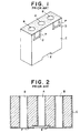
- FIGS. 1 and 2 of the accompanying drawings show a conventional dielectric filter of the above identified type with three resonators A and B, wherein a pair of input/output pads P are provided on a lateral side surface of the dielectric ceramic block, arranged at locations close to the open circuit end surface of the dielectric ceramic block and facing the respective outer resonators B and capacitively coupled to the respective outer resonatora B, each of said input/output pads P being separated from the outer conductor C by an insulating zone D surrounding it.
- Such conventional dielectric filter is disclosed in US Patent No. 5,146,193.
- each of the resonators A and B is normally made to have a length equal to 1/4 or a quarter of the specified resonant frequency
- the above arrangement of input/output pads P disposed vis-a-vis the respective outer resonators B at locations close to the open circuit end surface gives rise to a problem that the resonant frequency of the outer resonators B is increased due to the provision of the input/output pads P separated from the outer conductor C by respective insulating zones D and the partial removal of the outer conductor and consequently the resonant frequency of the outer resonators comes to disagree with that of the central resonator A at the cost of filtering performance.
- FIG. 2 of Japanese Patent Kokai No. 62-104201 discloses one example of this frequency compensating method.
- a conductive film F is formed on the short circuit end surface of the dielectric ceramic block in such known dielectric filter and connected to the edges of the other opening ends of the resonators on the short circuit end surface.
- the conductive film F is typically prepared by a screen printing which is adapted to mass production.
- the screen printing technique cannot feasibly be used and the conductive film F has to be formed by applying a conductive material to that side by means of a brush at the cost of manufacturing efficiency. In short, such a configuration is not adapted to mass production.
- a dielectric filter comprising a dielectric ceramic block, three or more than three resonators formed by boring so many through holes in the dielectric ceramic block and coating the peripheral walls thereof with an inner conductor, an outer conductor covering a specific area of the outer peripheral surface of the dielectric ceramic block excepting one end surface of the dielectric ceramic block which forms an open circuit end surface on which one opening ends of the through holes are positioned, and a pair of input/output pads formed on a lateral side surface of the dielectric ceramic block, arranged at locations close to the open circuit end surface of the dielectric ceramic block and facing the respective outermost resonators and capacitively coupled to the respective outermost resonators, each of said input/output pads being separated from the outer conductor by an insulating zone surrounding it, characterized in that additional conductors are provided on the open circuit end surface of said dielectric ceramic block, which extend from edges of the one opening ends of the outermost resonators for increasing the resonant length of each of the
- Each of the additional conductors may be outwardly extended along an axis across all the resonators.
- each additional conductor may be extended in one or two directions perpendicular to the axis across the resonators.
- Each of the additional conductors may have a width substantially equal to the diameter of the respective through holes.
- the outermost resonators are made to have a length slighter longer than the length corresponding to their proper resonant frequency in order to show a low initial resonant frequency. Then, the effect of the upward shift of the resonant frequency of the outermost resonators caused by the input/output pads that are formed close to the open circuit end surface of the dielectric ceramic block and separated from the outer conductor by respective insulating zones is offset by the low initial resonant frequency so that a dielectric filter having a proper resonant frequency will be realized.
- FIGS. 3 and 4 illustrate a first embodiment of a dielectric filter according to the present invention, which is a three stage type dielectric filter la comprising a dielectric ceramic block 2 on which three resonators 3a and 3b are provided.
- the dielectric ceramic block 2 of the dielectric filter 1a is rectangularly parallelepipedic having six outer surfaces 2a, 2b, 2c, 2d, 2e and 2f, and made of a titanium oxide type ceramic material.
- the resonators 3a and 3b are arranged in parallel with each other between the lateral side surfaces 2c and 2d of the block 2. They are formed by covering the peripheral walls of through holes 4a and 4b provided on the dielectric ceramic block 2 with respective inner conductors 5.
- the outer surfaces 2b, 2c, 2d, 2e and 2f of the dielectric ceramic block 2 are coated with an outer conductor 6 except the outer surface 2a which forms an open circuit end surface on which the corresponding opening ends of the through holes 4a and 4b are positioned.
- the outer conductor 6 operates as a shield electrode.
- Each of the resonators 3a and 3b has a length substantially equal to 1/4 or a quarter of the specified resonant frequency for an intended dielectric filter.
- a pair of input/output pads 7 are formed on the lateral side surface 2f of the dielectric ceramic block 2, arranged at locations close to the open circuit end surface 2a of the dielectric ceramic block 2 and facing the respective outer resonators 3b and capacitively coupled to the respective outer resonators 3b.
- Each of said input/ output pads 7 is separated from the outer conductor 6 by an insulating zone 8 surrounding it.
- the input/output pads 7 will be electrically connected to an electric path on a printed circuit board not shown.
- the input/ output pads 7 formed on the lateral side surface 2f of the dielectric ceramic block 2 at locations facing the respective outer resonators 3b raise the resonant frequency of the resonators 3b. Since the conductor lengths defined respectively by the through holes 4a and 4b of the resonators 3a and 3b are identical with each other, the provision of the input/output pads 7 makes the resonant frequency of the resonators 3b higher than that of the central resonator 3a. Consequently, such a dielectric filter does not provide a satisfactory filtering effect.
- frequency adjusting or compensating conductors 9 are provided on the open circuit end surface 2a of the dielectric ceramic block 2, which are extended from the inner conductors 5 of the respective outer resonators 3b to increase the effective resonant length of the outer resonators 3b.
- each conductor 9 is outwardly extended along the axis across the three resonators 3a and 3b and has a width substantially equal to the diameter of the respective through holes 4b.
- This arrangement is advantageous to produce an intended dielectric filter because each of the additional conductors 9 may be easily produced without requiring very high accuracy in the positioning thereof.
- the extension lenght of each conductor 9 may be determined in dependence on the design for an intended dielectric filter.
- the effect of raising the resonant frequency of the outer resonators 3b by the input/output pads 7 arranged on a lateral side surface 2f of the dielectric ceramic block 2 at locations close to the open circuit end surface 2a of the block 2 and facing the respective outer resonators 3b can be offset by the above arrangement of the extended conductors 9 for increasing the effective resonant length and hence lowering the resonant frequency of the outer resonators 3b in advance to achieve a resonant frequency substantially equal to 1/4 to the dielectric filter and the resonant frequencies of the resonators can be made substantially agree with each other.
- FIG. 5 illustrates a dielectric filter 1b according to another embodiment of the present invention.
- the frequency adjusting or compensating conductors 9 are formed by extending the respective outer resonators sideways in two directions, that is the conductors 9 are provided so that they are extended along two directions perpendicular to the axis across the three resonators 3a and 3b.
- the conductors 9 may be provided to be extended only in one direction perpendicular to the axis across the three resonators 3a and 3b.
- resonators 3a and 3b of the above embodiments have a circular cross section, they may alternatively have a cross section that is square or of some other geometric form.
- any of the embodiments of dielectric filter according to the invention comprising a pair of input/output pads arranged on a lateral side surface of the dielectric ceramic block at locations close to the open circuit end surface and facing the respective outer resonators, each of said input/output pads being separated from the outer conductor by an insulating zone surrounding it, the effect of raising the resonant frequency of the outer resonators by the provision of the input/output pads can be offset by the provision of extended conductors for increasing the effective resonant length and hence lowering the resonant frequency of the outer resonators in advance.
- such a dielectric filter can minimize the adverse effect of the input/output pads and the resonant frequencies of the resonators can be made substantially agree with each other.
Landscapes
- Physics & Mathematics (AREA)
- Electromagnetism (AREA)
- Control Of Motors That Do Not Use Commutators (AREA)
Abstract
Description
Claims (4)
- A dielectric filter comprising a dielectric ceramic block (2), three or more than three resonators (3a, 3b) formed by boring so many through holes (4a, 4b) in the dielectric ceramic block (2) and coating the peripheral walls thereof with an inner conductor (5), an outer conductor (6) covering a specific area (2b, 2c, 2d, 2e, 2f) of the outer peripheral surface (2a, 2b, 2c, 2d, 2e, 2f) of the dielectric ceramic block (2) excepting one end surface (2a) of the dielectric ceramic block (2) which forms an open circuit end on which one opening ends of the through holes (4a, 4b) are positioned, and a pair of input/output pads (7) formed on a lateral side surface (2f) of the dielectric ceramic block (2), arranged at locations close to the open circuit end surface (2a) of the dielectric ceramic block (2) and facing the respective outermost resonators (3b) and capacitively coupled to the respective outermost resonators (3b), each of said input/output pads (7) being separated from the outer conductor (6) by an insulating zone (8) surrounding it,
characterized in that additional conductors (9) are provided on the open circuit end suface (2a) of said dielectric ceramic block (2), which extend from edges of the one opening ends of the outermost resonators (3b) for increasing the resonant length of each of the outermost resonators (3b). - A dielectric filter as claimed in claim 1,
characterized in that said each additional conductor (9) is outwardly extended along an axis across all the resonators (3a, 3b). - A dielectric filter as claimed in claim 1,
characterized in that said each additional conductor (9) is extended in two directions perpendicular to an axis across the resonators (3a, 3b). - A dielectric filter as claimed in any one of claim 1 to 3, characterized in that said each additional conductor (9) has a width substantially equal to the diameter of the respective through holes (4b).
Applications Claiming Priority (3)
| Application Number | Priority Date | Filing Date | Title |
|---|---|---|---|
| JP8297518A JPH10126105A (en) | 1996-10-18 | 1996-10-18 | Dielectric filter |
| JP29751896 | 1996-10-18 | ||
| JP297518/96 | 1996-10-18 |
Publications (3)
| Publication Number | Publication Date |
|---|---|
| EP0837518A2 true EP0837518A2 (en) | 1998-04-22 |
| EP0837518A3 EP0837518A3 (en) | 1999-03-03 |
| EP0837518B1 EP0837518B1 (en) | 2002-11-20 |
Family
ID=17847565
Family Applications (1)
| Application Number | Title | Priority Date | Filing Date |
|---|---|---|---|
| EP97308223A Expired - Lifetime EP0837518B1 (en) | 1996-10-18 | 1997-10-16 | Dielectric filter |
Country Status (4)
| Country | Link |
|---|---|
| US (1) | US5936491A (en) |
| EP (1) | EP0837518B1 (en) |
| JP (1) | JPH10126105A (en) |
| DE (1) | DE69717233T2 (en) |
Families Citing this family (1)
| Publication number | Priority date | Publication date | Assignee | Title |
|---|---|---|---|---|
| JP6812670B2 (en) | 2016-06-17 | 2021-01-13 | Tdk株式会社 | Dielectric filter |
Citations (3)
| Publication number | Priority date | Publication date | Assignee | Title |
|---|---|---|---|---|
| JPS6052102A (en) * | 1983-09-01 | 1985-03-25 | Oki Electric Ind Co Ltd | Dielectric resonator and method for adjusting resonance frequency of dielectric resonator |
| JPS60152102A (en) * | 1984-01-19 | 1985-08-10 | Murata Mfg Co Ltd | Distributed constant type filter |
| US5525946A (en) * | 1993-09-16 | 1996-06-11 | Murata Manufacturing Co., Ltd. | Dielectric resonator apparatus comprising a plurality of one-half wavelength dielectric coaxial resonators having open-circuit gaps at ends thereof |
Family Cites Families (8)
| Publication number | Priority date | Publication date | Assignee | Title |
|---|---|---|---|---|
| JPS60254802A (en) * | 1984-05-30 | 1985-12-16 | Murata Mfg Co Ltd | Distributed constant type filter |
| US4768003A (en) * | 1984-09-28 | 1988-08-30 | Oki Electric Industry Co., Inc. | Microwave filter |
| JPS62104201A (en) * | 1985-10-30 | 1987-05-14 | Fujitsu Ltd | Dielectric filter |
| JPS63171100A (en) * | 1987-01-09 | 1988-07-14 | Mitsubishi Pencil Co Ltd | Production of diaphragm for total carbonaceous speaker |
| US4745379A (en) * | 1987-02-25 | 1988-05-17 | Rockwell International Corp. | Launcher-less and lumped capacitor-less ceramic comb-line filters |
| JPH0713284Y2 (en) * | 1987-09-21 | 1995-03-29 | 株式会社村田製作所 | Resonant frequency adjustment structure for integrally molded dielectric filter |
| US5146193A (en) * | 1991-02-25 | 1992-09-08 | Motorola, Inc. | Monolithic ceramic filter or duplexer having surface mount corrections and transmission zeroes |
| US5218329A (en) * | 1992-03-25 | 1993-06-08 | Motorola, Inc. | Low profile ceramic filter with self aligning shield |
-
1996
- 1996-10-18 JP JP8297518A patent/JPH10126105A/en active Pending
-
1997
- 1997-10-16 DE DE69717233T patent/DE69717233T2/en not_active Expired - Fee Related
- 1997-10-16 EP EP97308223A patent/EP0837518B1/en not_active Expired - Lifetime
- 1997-10-17 US US08/953,233 patent/US5936491A/en not_active Expired - Fee Related
Patent Citations (3)
| Publication number | Priority date | Publication date | Assignee | Title |
|---|---|---|---|---|
| JPS6052102A (en) * | 1983-09-01 | 1985-03-25 | Oki Electric Ind Co Ltd | Dielectric resonator and method for adjusting resonance frequency of dielectric resonator |
| JPS60152102A (en) * | 1984-01-19 | 1985-08-10 | Murata Mfg Co Ltd | Distributed constant type filter |
| US5525946A (en) * | 1993-09-16 | 1996-06-11 | Murata Manufacturing Co., Ltd. | Dielectric resonator apparatus comprising a plurality of one-half wavelength dielectric coaxial resonators having open-circuit gaps at ends thereof |
Non-Patent Citations (2)
| Title |
|---|
| PATENT ABSTRACTS OF JAPAN vol. 9, no. 181 (E-331), 26 July 1985 & JP 60 052102 A (OKI DENKI KOGYO KK), 25 March 1985 * |
| PATENT ABSTRACTS OF JAPAN vol. 9, no. 318 (E-366), 13 December 1985 & JP 60 152102 A (MURATA SEISAKUSHO : KK), 10 August 1985 * |
Also Published As
| Publication number | Publication date |
|---|---|
| JPH10126105A (en) | 1998-05-15 |
| US5936491A (en) | 1999-08-10 |
| EP0837518A3 (en) | 1999-03-03 |
| DE69717233D1 (en) | 2003-01-02 |
| DE69717233T2 (en) | 2003-08-28 |
| EP0837518B1 (en) | 2002-11-20 |
Similar Documents
| Publication | Publication Date | Title |
|---|---|---|
| JP3239552B2 (en) | Dielectric resonator device | |
| US5926078A (en) | Dielectric filter including various means of adjusting the coupling between resonators | |
| US20010040490A1 (en) | Transmission line and transmission line resonator | |
| JPH04352305A (en) | Method of adjusting three layer structured spiral inductor | |
| EP0809315A1 (en) | Dielectric filter | |
| JP2003298313A (en) | Dielectric electronic component such as dielectric filter or dielectric duplers, etc., and coupling quantity adjusting method for the dielectric electronic component | |
| US5696473A (en) | Dielectric filter having a non-right angle stepped end surface | |
| US5945895A (en) | Resonant frequency compensated dielectric filter | |
| EP0837518B1 (en) | Dielectric filter | |
| JP3450926B2 (en) | Dielectric filter and method of adjusting frequency bandwidth thereof | |
| EP0635897B1 (en) | Dielectric filter | |
| US5291162A (en) | Method of adjusting frequency response in a microwave strip-line filter device | |
| US5939959A (en) | Dielectric filter with elevated inner regions adjacent resonator openings | |
| EP0798803B1 (en) | Dielectric filter | |
| JP2661007B2 (en) | Dielectric filter and pass band adjustment method thereof | |
| JPS63283201A (en) | Integrally molded type high frequency filter | |
| JP3213987B2 (en) | Dielectric resonator and method for adjusting characteristics thereof | |
| EP0827232B1 (en) | Dielectric filter | |
| JPH08321702A (en) | Dielectric filter and adjustment method for its frequency band with | |
| JP2725904B2 (en) | Frequency Adjustment Method of Microwave Stripline Filter | |
| JPH06164206A (en) | Dielectric filter and combination structure of dielectric filter and circuit board | |
| KR100213374B1 (en) | Small dielectric filter | |
| JP2003298310A (en) | Dielectric filter | |
| JPH09321503A (en) | Dielectric filter | |
| JPH06140807A (en) | Dielectric filter |
Legal Events
| Date | Code | Title | Description |
|---|---|---|---|
| PUAI | Public reference made under article 153(3) epc to a published international application that has entered the european phase |
Free format text: ORIGINAL CODE: 0009012 |
|
| AK | Designated contracting states |
Kind code of ref document: A2 Designated state(s): DE FR GB |
|
| PUAL | Search report despatched |
Free format text: ORIGINAL CODE: 0009013 |
|
| AK | Designated contracting states |
Kind code of ref document: A3 Designated state(s): AT BE CH DE DK ES FI FR GB GR IE IT LI LU MC NL PT SE |
|
| 17P | Request for examination filed |
Effective date: 19990715 |
|
| AKX | Designation fees paid |
Free format text: DE FR GB |
|
| GRAG | Despatch of communication of intention to grant |
Free format text: ORIGINAL CODE: EPIDOS AGRA |
|
| 17Q | First examination report despatched |
Effective date: 20020214 |
|
| GRAG | Despatch of communication of intention to grant |
Free format text: ORIGINAL CODE: EPIDOS AGRA |
|
| GRAH | Despatch of communication of intention to grant a patent |
Free format text: ORIGINAL CODE: EPIDOS IGRA |
|
| GRAH | Despatch of communication of intention to grant a patent |
Free format text: ORIGINAL CODE: EPIDOS IGRA |
|
| GRAA | (expected) grant |
Free format text: ORIGINAL CODE: 0009210 |
|
| AK | Designated contracting states |
Kind code of ref document: B1 Designated state(s): DE FR GB |
|
| REG | Reference to a national code |
Ref country code: GB Ref legal event code: FG4D |
|
| REF | Corresponds to: |
Ref document number: 69717233 Country of ref document: DE Date of ref document: 20030102 |
|
| ET | Fr: translation filed | ||
| PLBE | No opposition filed within time limit |
Free format text: ORIGINAL CODE: 0009261 |
|
| STAA | Information on the status of an ep patent application or granted ep patent |
Free format text: STATUS: NO OPPOSITION FILED WITHIN TIME LIMIT |
|
| 26N | No opposition filed |
Effective date: 20030821 |
|
| PGFP | Annual fee paid to national office [announced via postgrant information from national office to epo] |
Ref country code: DE Payment date: 20071011 Year of fee payment: 11 |
|
| PGFP | Annual fee paid to national office [announced via postgrant information from national office to epo] |
Ref country code: GB Payment date: 20071010 Year of fee payment: 11 Ref country code: FR Payment date: 20071009 Year of fee payment: 11 |
|
| GBPC | Gb: european patent ceased through non-payment of renewal fee |
Effective date: 20081016 |
|
| REG | Reference to a national code |
Ref country code: FR Ref legal event code: ST Effective date: 20090630 |
|
| PG25 | Lapsed in a contracting state [announced via postgrant information from national office to epo] |
Ref country code: DE Free format text: LAPSE BECAUSE OF NON-PAYMENT OF DUE FEES Effective date: 20090501 |
|
| PG25 | Lapsed in a contracting state [announced via postgrant information from national office to epo] |
Ref country code: FR Free format text: LAPSE BECAUSE OF NON-PAYMENT OF DUE FEES Effective date: 20081031 |
|
| PG25 | Lapsed in a contracting state [announced via postgrant information from national office to epo] |
Ref country code: GB Free format text: LAPSE BECAUSE OF NON-PAYMENT OF DUE FEES Effective date: 20081016 |