EP0836246B1 - Système de détrompage pour connecteur électrique - Google Patents
Système de détrompage pour connecteur électrique Download PDFInfo
- Publication number
- EP0836246B1 EP0836246B1 EP96116390A EP96116390A EP0836246B1 EP 0836246 B1 EP0836246 B1 EP 0836246B1 EP 96116390 A EP96116390 A EP 96116390A EP 96116390 A EP96116390 A EP 96116390A EP 0836246 B1 EP0836246 B1 EP 0836246B1
- Authority
- EP
- European Patent Office
- Prior art keywords
- keying
- frame
- cable plug
- sidewalls
- housing
- Prior art date
- Legal status (The legal status is an assumption and is not a legal conclusion. Google has not performed a legal analysis and makes no representation as to the accuracy of the status listed.)
- Expired - Lifetime
Links
Images


Classifications
-
- H—ELECTRICITY
- H01—ELECTRIC ELEMENTS
- H01R—ELECTRICALLY-CONDUCTIVE CONNECTIONS; STRUCTURAL ASSOCIATIONS OF A PLURALITY OF MUTUALLY-INSULATED ELECTRICAL CONNECTING ELEMENTS; COUPLING DEVICES; CURRENT COLLECTORS
- H01R13/00—Details of coupling devices of the kinds covered by groups H01R12/70 or H01R24/00 - H01R33/00
- H01R13/64—Means for preventing incorrect coupling
-
- H—ELECTRICITY
- H01—ELECTRIC ELEMENTS
- H01R—ELECTRICALLY-CONDUCTIVE CONNECTIONS; STRUCTURAL ASSOCIATIONS OF A PLURALITY OF MUTUALLY-INSULATED ELECTRICAL CONNECTING ELEMENTS; COUPLING DEVICES; CURRENT COLLECTORS
- H01R13/00—Details of coupling devices of the kinds covered by groups H01R12/70 or H01R24/00 - H01R33/00
- H01R13/648—Protective earth or shield arrangements on coupling devices, e.g. anti-static shielding
- H01R13/658—High frequency shielding arrangements, e.g. against EMI [Electro-Magnetic Interference] or EMP [Electro-Magnetic Pulse]
-
- H—ELECTRICITY
- H01—ELECTRIC ELEMENTS
- H01R—ELECTRICALLY-CONDUCTIVE CONNECTIONS; STRUCTURAL ASSOCIATIONS OF A PLURALITY OF MUTUALLY-INSULATED ELECTRICAL CONNECTING ELEMENTS; COUPLING DEVICES; CURRENT COLLECTORS
- H01R12/00—Structural associations of a plurality of mutually-insulated electrical connecting elements, specially adapted for printed circuits, e.g. printed circuit boards [PCB], flat or ribbon cables, or like generally planar structures, e.g. terminal strips, terminal blocks; Coupling devices specially adapted for printed circuits, flat or ribbon cables, or like generally planar structures; Terminals specially adapted for contact with, or insertion into, printed circuits, flat or ribbon cables, or like generally planar structures
- H01R12/70—Coupling devices
- H01R12/7005—Guiding, mounting, polarizing or locking means; Extractors
Definitions
- This invention generally relates to the art of electrical connectors and, particularly, to an electrical connector keying system according to the preamble of claim 1.
- a shielded electrical connector assembly is known from EP-A-0,624,928 which has the features of the preamble to claim 1.
- a cable connector is shown including an outer shielding housing having a pair of grooves each on the top and bottom sides of the connector body. The grooves in the pairs have different distances, and these distances correspond to the distances between pairs of grounding ribs in a conductive housing which defines receptacle means. The grooves and the ribs form a polarizing feature for the cable connector which therefore can be inserted into the receptacle means only in one orientation.
- a keying system may require that a given plug connector be inserted only into a particular receptacle, while preventing other plug connectors from being inserted into that receptacle.
- Such keying systems are akin to polarizing systems which require one connector to be mated in only a given orientation to ensure that mating terminals are properly engaged.
- Such keying systems often include selected arrays of keying protrusions movable into keying recesses only if the array or arrangement of keying protrusions match the arrangement of keying recesses.
- One of the problems with any such keying system is the expenses involved.
- a connector keying system is known from US-A-4,832,625.
- the plug housing molded of thermoplastic resin contains a plurality of keying projections extending outwardly and being connected to the housing through flexible hinges and frangible webs.
- the receptacle housing is molded of thermoplastic material and includes key-receiving grooves which have respective latent blocking members assigned thereto.
- the keying projections of the plug can be deflected and made ineffective.
- this blocking member can be moved into the respective groove and block same. In this manner, different configurations of projections and grooves can be established so that only selected pairs of plugs and receptacles can be mated with one another whereas others are excluded. See also as an example document EP-A-0 595 304.
- An object, therefore, of the invention is to provide a new and improved keying system in an electrical connector arrangement.
- the invention is defined in claim 1.
- the present invention is directed to solving these problems in a unique system which greatly reduces the costs of manufacture.
- the invention is disclosed in a cable or connector plug which includes a housing that can be standard for all connectors, with only a face plate of the housing having to be changed to change the keying system.
- the keying system is disclosed in a shielded transmission system which includes a stamped and formed conductive receptacle having a plurality of unbent keying tabs which simply can be bent to achieve a plurality of different keying arrangements. Alternatively, prebent tabs can be cut also to achieve different keying configurations.
- the keying system is disclosed in a grounding shroud assembly for receiving a cable plug.
- the cable plug includes a housing having at least one keying recess at a selected location on a side thereof.
- a grounding shroud assembly includes a conductive frame having a base and at least a pair of sidewalls extending from the base and defining a receptacle for receiving the cable plug. At least one of the sidewalls has at least one keying protrusion for extending into the keying recess.
- a conductive spring is disposed about the conductive frame and the at least one of the sidewalls.
- the frame is stamped and formed of metal material
- the keying protrusion comprises a tab bent inwardly of the at least one sidewall.
- the sidewall includes a plurality of stamped unbent tabs, whereby any one or more of the tabs can be bent inwardly to form one or more of the keying protrusions.
- the conductive spring is generally U-shaped
- the conductive frame is generally U-shaped and nested within the U-shaped spring.
- the invention contemplates a unique system wherein the housing of the cable plug includes a plurality of keying grooves on at least one side thereof.
- a face plate is mounted on the housing and includes at least one notch in alignment with a respective one of the keying grooves to define the keying recess. Other of the keying grooves in the housing are blocked by the face plate. Therefore, the face plate can be interchanged without changing the entire housing, to accommodate different arrays of keying protrusions. This saves considerable manufacturing and inventory costs.
- novel concepts of the invention are not limited to a grounding shroud assembly for receiving a cable plug.
- the invention is equally applicable for a wide range of electrical connector arrangements or systems.
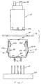
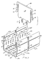
- the invention is embodied in a grounding shroud assembly, generally designated 12.
- the assembly is shown in Figure 1 for mounting in an opening 14 in a panel 16 and for receiving a cable plug, generally designated 18, on one side of the panel and contact pins 20 from a printed circuit board 22 on the opposite side of the panel.
- FIG. 2 shows grounding shroud assembly 12 mounted in opening 14 in panel 16. The assembly also is shown in Figure 2 mounted on printed circuit board 22 with contact pins 20 projecting into the shroud assembly. Cable plug 18 is insertable into the shroud assembly in the direction of arrow "A".
- printed circuit board 22 is of a generally conventional configuration, with conventional contact pins 20 projecting therefrom.
- Panel 16 is fabricated of conductive material and is part of a shielding casing for protecting components, such as electrical components on the printed circuit board, against electrical emissions and radiations.
- cable plug 18 also is of a conventional construction with an outer shield and mounts a plurality of female terminals for receiving contact pins 20. The female terminals are terminated to conductors within shielded or coaxial cables 24.
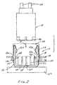
- grounding shroud assembly 12 includes two main components, namely a frame, generally designated 26, and one or more springs, generally designated 28.
- the shroud assembly shown herein is designed for receiving a pair of cable plugs and, therefore, a divider plate (described hereinafter) is used to divide frame 26 into two distinct receptacles for the two plugs.
- a divider plate (described hereinafter) is used to divide frame 26 into two distinct receptacles for the two plugs.
- two separate springs 28 are employed.
- frame 26 of grounding shroud assembly 12 is generally U-shaped and includes a base or bottom wall 30 and a pair of sidewalls 32 extending upwardly from the base.
- the frame is stamped and formed of conductive sheet metal material, such as brass, and base 30 and sidewalls 32 define a receptacle therebetween for receiving one or more of the cable plugs 18.
- Frame 26 also includes a plurality of apertures 34, 36 and 38 therethrough for receiving contact pins 20 from printed circuit board 22.
- Apertures 34 are generally rectangular and freely receive ground pins from the printed circuit board.
- Apertures 36 are circular and also freely receive ground pins from the printed circuit board.
- Apertures 38 are circular and larger than apertures 36 and receive signal contact pins from the printed circuit board.
- Frame 26 further includes slots 40 in sidewalls 32, along with notches 42 in the upper edges of the sidewalls.
- the slots and notches are provided for mounting a conductive divider plate, as described hereinafter.
- Tabs 44 project longitudinally outwardly from opposite ends of sidewalls 32, and base 30 includes notches 46 at opposite ends thereof.
- Tabs 44 are provided for mounting conductive end plates, as described hereinafter.
- Notches 46 facilitate mounting springs 28.
- keying tabs 48 are formed out of sidewalls 32 and are bent inwardly of the frame. Unbent keying tabs 48a also are shown in Figures 3 and 4. The keying tabs operate with keying means on cable plugs 18, as described hereinafter.
- each spring 28 is stamped and formed of conductive spring metal, such as beryllium copper, and includes a base 50 and a pair of upstanding sidewalls 52 extending from the base for embracing the generally U-shaped frame 26.
- Sidewalls 52 have protrusions in the form of integral outwardly bowed portions 52a for engaging inner edges of opening 14 in panel 16 to mount the grounding shroud assembly in the panel as shown in Figure 2.
- the spring also includes integral, inwardly bowed portions 52b which extend around and into the inside of sidewalls 32 of frame 26 for frictionally and electrically engaging the outer shield of the cable plug 18.
- Each spring 28 of grounding shroud assembly 12 includes a plurality of apertures 54, 56 and 58 through base 50 of the spring.
- Apertures 54 are H-shaped to define a pair of opposing tabs 54a which deform and grip the ground contact pins which extend therethrough. This functions to mount the grounding shroud assembly onto printed circuit board 22 as shown in Figure 2.
- Apertures 56 are circular and freely receive the remainder of the ground pins from the printed circuit board. All of the apertures for receiving the ground pins are not H-shaped in order to avoid excessive mounting forces.
- Apertures 58 freely receive the signal contact pins from the printed circuit board.
- H-shaped apertures 54 in base 50 of spring 28 register with rectangular apertures 34 in base 30 of frame 26; smaller round apertures 56 in the spring(s) register with smaller round apertures 36 in the frame and larger round apertures 58 in the spring register with larger round apertures 38 in the frame.
- a tab 60 projects outwardly from base 50 at the end of each spring 28, for purposes to be described hereinafter.
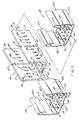
- U-shaped conductive springs 28 are mounted on U-shaped conductive frame 26 by sliding the springs onto opposite ends of the frame in the direction of arrows "B" in Figure 3.
- Figure 6 shows the two springs fully mounted on and embracing the frame. Once in their fully mounted positions, tabs 60 at the ends of bases 50 of the springs are bent into notches 46 in base 30 of the frame.
- Figures 6A and 6B show contact pins from the printed circuit board inserted into the apertures in the base of the spring and the base of frame of grounding shroud assembly 12. More particularly, contact pin 20A in Figures 6A and 6B designates a ground pin inserted through H-shaped aperture 54 in the spring and through rectangular aperture 34 in the frame. Opposing tabs 54a grip the ground pin to effectively mount the grounding shroud assembly onto the printed circuit board. Contact pin 20B in Figures 6A and 6B represents another ground pin from the printed circuit board which extends freely through small round aperture 56 in the spring and small round aperture 36 in the frame.
- Contact pin 20C in Figures 6A and 6B represents a signal pin from the printed circuit board extending freely through larger round aperture 58 in the spring and larger round aperture 38 in the frame.
- the signal pins pass through larger apertures which are adapted to the impedance characteristics to be achieved with the connector arrangement.
- a divider plate generally designated 66, is shown to include a generally planar body 68 having a pair of mounting legs 70 projecting downwardly therefrom.
- a pair of arms 72 are spaced outwardly from opposite edges of the body to define grooves 74.
- the arms terminate in outwardly projecting stop flanges 76.
- the divider plate is stamped from conductive sheet metal material approximately the same thickness as the sheet metal material of frame 26.
- Divider plate 66 is mounted onto frame 26 in the direction of arrow "C" (Fig. 7) until the divider plate assumes a position shown in Figure 8, dividing the frame into two distinct receptacles for a pair of cable plugs 18.
- sidewalls 32 of the frame move into grooves 74 inside arms 72 of the divider plate, until the bottoms of the grooves seat into notches 42 at the tops of the sidewalls of the frame.
- Mounting legs 70 at the bottom of the divider plate extend into mounting holes 78 (Fig. 8) in printed circuit board 22.
- Figure 8 also shows that a pair of end plates, generally designated 80, are used to close the ends of the grounding shroud assembly.
- End plates 80 are of substantially identical construction to divider plate 66 and, accordingly, like reference numerals have been applied to like portions of the end plates corresponding to the same portions of the divider plate. It can be seen in Figure 8 that the end plates are mounted at the opposite ends of frame 26, with tabs 44 at the opposite ends of sidewalls 32 of the frame press fit into grooves 74 inside arms 72 of the end plates. Mounting legs 70 of the end plates project into mounting holes 78 in printed circuit board 22.
- the frame With frame 26 being fabricated of a thicker more robust material, such as brass or the like, the frame provides a sturdy structure forming the receptacles for receiving the cable plugs.
- Springs 28 being fabricated of a thinner springy material, such as beryllium copper or the like, provides a yielding structure for mounting in the panel opening, as well as gripping the plugs and the contact pins in H-shaped apertures 54. Moreover, the unbreached surface of the springs 28 provides shielding against emissions and radiations which the openings provided by the keying tabs 48, 48a may otherwise permit to pass.
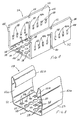
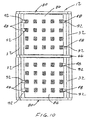
- Figure 9 shows cable plug 18 to include a mating end face 82 having a plurality of passages 84 for receiving contact pins 20 from printed circuit board 22.
- the passages lead to a plurality of female terminals or contacts within the cable plug and which mate with the contact pins.
- Mating face 82 is defined by a face 86 mounted on a dielectric housing 88 of the cable plug.
- Grounding shroud assembly 12 described above in relation to Figures 1-8 and cable plugs 18 include a unique keying system to prevent any given cable plug from being inserted into a wrong receptacle or side of grounding shroud assembly 12. More particularly, Figure 10 shows that opposite sides of housing 88 of the cable plug is provided with a plurality of keying grooves 90. Face plate 86 is provided with a plurality of keying notches 92. The keying notches align with selected ones of keying grooves 90. For instance, in Figure 9, keying grooves 92 at the top of face plate 86 are aligned with the outermost keying grooves 80 of the housing.
- keying notches 92 at the bottom of face plate 86 are aligned with the first and third keying grooves at the bottom of the housing, as looking from the left in the depiction. Therefore, the top of the cable plug may be keyed differently from the bottom of the cable plug.
- face plate 86 in Figure 9A is provided with two keying notches at the right-hand end thereof, and face plate 86 in Figure 9B is provided with two keying notches 92 at the left-hand end thereof. Therefore, the cable plug shown in Figure 9A is keyed different from the cable plug shown in Figure 9B.
- plug housing 88 with a plurality of keying grooves 90 as shown in Figure 9, only some or all of the keying grooves can be exposed for receiving keying tabs 48 of the shroud assembly, simply by changing face plate 86 and its respective, selected arrangement of keying notches 92. Therefore, the entire plug housing does not have to be changed to change the keying arrangement. Only the face plate 86, with a selected arrangement of keying notches 92, must be changed to change the keying system. Similarly, keying tabs 48 in the sidewalls 32 of frame 26 easily are bent inwardly or cut at selected locations corresponding to the locations of the keying notches in the respective cable plug. The keying tabs 48 can be cut with a small cutting tool even when the spring 28 is already in position and preventing access to the exterior of the frame 26.
Landscapes
- Details Of Connecting Devices For Male And Female Coupling (AREA)
Claims (12)
- Système de détrompage pour permettre d'accoupler une fiche (18) de câble uniquement avec un moyen à prise appropriée, comportantcaractérisé en ce quela fiche (18) de câble comprenant un boítier (88) ayant au moins un évidement de détrompage (90, 92) dans une position choisie sur l'un de ses côtés ; etle moyen à prise destiné à recevoir la fiche (18) de câble comprenant au moins une paire de parois latérales (32) et une rangée de saillies de détrompage qui sont conçues pour coopérer avec le, au moins un, évidement de détrompage,
les saillies de détrompage comprennent des languettes métalliques repliables (48) sur au moins l'une des parois latérales, au moins l'une des languettes de détrompage (48) étant pliée vers l'intérieur pour s'adapter à l'évidement de détrompage (90, 92) de la fiche afin de faire saillie dans le trajet dudit évidement de détrompage lorsque la fiche de câble est introduite dans le moyen à prise. - Système de détrompage selon la revendication 1,
dans lequel ledit moyen à prise est un ensemble à coque (12) de mise à la masse comprenant un bâti conducteur (26) ayant une base (30) et ladite paire de parois latérales (32). - Système de détrompage selon la revendication 1 ou 2,
dans lequel ladite fiche (18) de câble et ledit moyen à prise appartiennent à un agencement de connecteur électrique,
ledit boítier (88) de ladite fiche (18) de câble ayant une plaque frontale (86) montée sur ce boítier et comprenant au moins une encoche de détrompage (92) en alignement avec une gorge respective de détrompage (90) sur la fiche (18) de câble afin de former ledit évidement de détrompage,
grâce à quoi la plaque frontale (86) peut être interchangée sans changer le boítier (88) pour recevoir différentes rangées de languettes de détrompage (48) sur le moyen à prise. - Système de détrompage selon l'une des revendications 2 ou 3,
comprenant un ressort conducteur (28) autour du bâti conducteur (26) et d'au moins l'une des parois latérales (32). - Système de détrompage selon l'une quelconque des revendications 1 à 4,
dans lequel ledit bâti (26) est découpé et formé en une matière métallique. - Système de détrompage selon l'une quelconque des revendications 2 à 5,
dans lequel ledit bâti (26) est de forme générale en U. - Système de détrompage selon la revendication 6,
dans lequel ledit ressort conducteur (28) est de forme générale en U, et ledit bâti conducteur (26) est logé dans le ressort de forme générale en U. - Système de détrompage selon l'une quelconque des revendications 5 à 7,
dans lequel ladite, au moins une, des parois latérales (32) du bâti (26) comporte une pluralité de languettes découpées non pliées (48a) conçues pour être pliées vers l'intérieur suivant une configuration souhaitée pour former une ou plusieurs desdites saillies de détrompage. - Système de détrompage selon l'une quelconque des revendications 1 à 8,
dans lequel ledit boítier (88) comporte plusieurs gorges de détrompage (90) sur au moins l'un de ses côtés. - Système de détrompage selon l'une quelconque des revendications 1 à 8,
dans lequel ledit boítier (88) comporte plusieurs gorges (90) de détrompage sur des côtés opposés de ce boítier. - Système de détrompage selon les revendications 3 et 9 ou 10,
dans lequel plusieurs desdites plaques frontales (86) sont prévues, comprenant chacune au moins une encoche (92) en alignement avec l'une, respective, de plusieurs des gorges de détrompage (90), la plaque frontale (86) étant telle qu'elle bloque toutes les autres gorges de détrompage (90) à l'exception de celles en alignement avec une encoche choisie (92),
la pluralité de plaques frontales (86) offrant différentes distributions des encoches (92) pour recevoir l'une, choisie, des différentes rangées de languettes de détrompage (48) sur le moyen à prise, l'une, choisie, des plaques frontales (86) étant montée sur le boítier (88) de la fiche de câble (18). - Système de détrompage selon l'une quelconque des revendications 2 à 11,
dans lequel l'ensemble à coque de mise à la masse (12) est conçu pour un montage dans une ouverture (14) dans un panneau (16) et pour recevoir la fiche de câble (18) sur un côté du panneau et des broches de contact (20) provenant d'une plaquette (22) à circuit imprimé sur un côté opposé du panneau,
dans lequel la base du bâti (26) est traversée par des ouvertures (34, 36, 38) destinées à recevoir les broches de contact (20),
la coque comportantun ressort conducteur (28) de forme générale en U comprenant une base (50) et au moins une paire de parois latérales (52) s'étendant depuis la base pour entourer le bâti (26) de forme générale en U et faciliter le montage de l'ensemble à coque (12) dans l'ouverture (14) du panneau (16), la base du ressort ayant des ouvertures (54, 56, 58) en alignement avec les ouvertures situées dans la base du bâti pour recevoir les broches de contact.
Priority Applications (6)
| Application Number | Priority Date | Filing Date | Title |
|---|---|---|---|
| DE69622408T DE69622408T2 (de) | 1996-10-12 | 1996-10-12 | Verschlüsselungssystem für elektrische Verbinder |
| EP96116390A EP0836246B1 (fr) | 1996-10-12 | 1996-10-12 | Système de détrompage pour connecteur électrique |
| TW087212307U TW392956U (en) | 1996-10-12 | 1997-10-09 | Electrical connector keying system |
| JP9314167A JP3057562B2 (ja) | 1996-10-12 | 1997-10-09 | 電気コネクタのキー機構 |
| CN97126221A CN1114249C (zh) | 1996-10-12 | 1997-10-11 | 电连接器的键合系统 |
| KR1019970052200A KR100291296B1 (ko) | 1996-10-12 | 1997-10-11 | 전기커넥터키잉시스템 |
Applications Claiming Priority (1)
| Application Number | Priority Date | Filing Date | Title |
|---|---|---|---|
| EP96116390A EP0836246B1 (fr) | 1996-10-12 | 1996-10-12 | Système de détrompage pour connecteur électrique |
Publications (2)
| Publication Number | Publication Date |
|---|---|
| EP0836246A1 EP0836246A1 (fr) | 1998-04-15 |
| EP0836246B1 true EP0836246B1 (fr) | 2002-07-17 |
Family
ID=8223292
Family Applications (1)
| Application Number | Title | Priority Date | Filing Date |
|---|---|---|---|
| EP96116390A Expired - Lifetime EP0836246B1 (fr) | 1996-10-12 | 1996-10-12 | Système de détrompage pour connecteur électrique |
Country Status (6)
| Country | Link |
|---|---|
| EP (1) | EP0836246B1 (fr) |
| JP (1) | JP3057562B2 (fr) |
| KR (1) | KR100291296B1 (fr) |
| CN (1) | CN1114249C (fr) |
| DE (1) | DE69622408T2 (fr) |
| TW (1) | TW392956U (fr) |
Cited By (2)
| Publication number | Priority date | Publication date | Assignee | Title |
|---|---|---|---|---|
| US10938157B2 (en) | 2018-06-08 | 2021-03-02 | Amphenol Assembletech (Xiamen) Co., Ltd | High speed electrical connector for compact electronic systems |
| US11128092B2 (en) | 2018-07-31 | 2021-09-21 | Amphenol Assembletech (Xiamen) Co., Ltd | Robust, miniaturized electrical connector |
Families Citing this family (4)
| Publication number | Priority date | Publication date | Assignee | Title |
|---|---|---|---|---|
| DE202014011219U1 (de) | 2013-12-12 | 2018-08-27 | Harting Electric Gmbh & Co. Kg | Halterahmen für einen Steckverbinder |
| DE102015101433B3 (de) * | 2015-02-02 | 2016-06-16 | Harting Electric Gmbh & Co. Kg | Halterahmen für Steckverbindermodule |
| CN106953188B (zh) * | 2017-02-21 | 2023-12-05 | 中航光电科技股份有限公司 | 一种转接连接器 |
| CN112397914B (zh) * | 2018-12-31 | 2021-09-07 | 深圳北芯生命科技股份有限公司 | 插件式连接装置 |
Family Cites Families (5)
| Publication number | Priority date | Publication date | Assignee | Title |
|---|---|---|---|---|
| FR2489609A1 (fr) * | 1980-08-26 | 1982-03-05 | Lb Air | Module de raccordement de conducteurs electriques a connecteurs amovibles |
| US4832625A (en) * | 1988-08-18 | 1989-05-23 | Amp Incorporated | Connector keying system |
| US5380216A (en) * | 1992-05-11 | 1995-01-10 | The Whitaker Corporation | Cable backpanel interconnection |
| EP0595304B1 (fr) * | 1992-10-29 | 1997-09-24 | Siemens Aktiengesellschaft | Dispositif de blindage pour connecteur de câble rectangulaire |
| EP0624928B1 (fr) * | 1993-05-14 | 1997-08-13 | Molex Incorporated | Ensemble connecteur électrique blindé |
-
1996
- 1996-10-12 DE DE69622408T patent/DE69622408T2/de not_active Expired - Fee Related
- 1996-10-12 EP EP96116390A patent/EP0836246B1/fr not_active Expired - Lifetime
-
1997
- 1997-10-09 TW TW087212307U patent/TW392956U/zh not_active IP Right Cessation
- 1997-10-09 JP JP9314167A patent/JP3057562B2/ja not_active Expired - Lifetime
- 1997-10-11 CN CN97126221A patent/CN1114249C/zh not_active Expired - Fee Related
- 1997-10-11 KR KR1019970052200A patent/KR100291296B1/ko not_active IP Right Cessation
Cited By (2)
| Publication number | Priority date | Publication date | Assignee | Title |
|---|---|---|---|---|
| US10938157B2 (en) | 2018-06-08 | 2021-03-02 | Amphenol Assembletech (Xiamen) Co., Ltd | High speed electrical connector for compact electronic systems |
| US11128092B2 (en) | 2018-07-31 | 2021-09-21 | Amphenol Assembletech (Xiamen) Co., Ltd | Robust, miniaturized electrical connector |
Also Published As
| Publication number | Publication date |
|---|---|
| DE69622408D1 (de) | 2002-08-22 |
| EP0836246A1 (fr) | 1998-04-15 |
| KR100291296B1 (ko) | 2001-06-01 |
| CN1114249C (zh) | 2003-07-09 |
| TW392956U (en) | 2000-06-01 |
| JPH10149858A (ja) | 1998-06-02 |
| JP3057562B2 (ja) | 2000-06-26 |
| CN1187702A (zh) | 1998-07-15 |
| KR19980032755A (ko) | 1998-07-25 |
| DE69622408T2 (de) | 2003-03-06 |
Similar Documents
| Publication | Publication Date | Title |
|---|---|---|
| EP0836249B1 (fr) | Enveloppe électrique de mise à la terre | |
| EP0569782B1 (fr) | Dispositif de contacts | |
| EP0700125B1 (fr) | Connecteur électrique avec dispositif secondaire de rétention des contacts | |
| EP1435126B1 (fr) | Ensemble connecteur a cles pour circuit flexible plat | |
| EP0761028B1 (fr) | Connecteur electrique avec guides | |
| US4781626A (en) | Keying system for connector families | |
| US5118306A (en) | Multi-conductor electrical connector | |
| US7331825B2 (en) | Electrical connector | |
| US5478253A (en) | Electrostatic discharge contacts for blind mating connectors | |
| US6095865A (en) | Modular jack | |
| US6217378B1 (en) | Universal serial bus connector | |
| CA2144704A1 (fr) | Connecteur combine | |
| EP3411928B1 (fr) | Connecteur enfichable à séparation galvanique intégrée et élément de blindage | |
| US5186639A (en) | Electrical connector with plug detection switch | |
| TW202110001A (zh) | 板端連接器和連接器組件 | |
| US7976321B2 (en) | Electrical connector with a ground terminal | |
| US6042398A (en) | Electrical connector having improved grounding arrangement | |
| EP0231539B1 (fr) | Assemblage de connecteurs électriques blindés et codés | |
| EP0836246B1 (fr) | Système de détrompage pour connecteur électrique | |
| US6458001B1 (en) | Receptacle connector having anti-mismating structures | |
| EP1315252B1 (fr) | Connecteur électrique avec système amélioré de décharge électrostatique | |
| US5827092A (en) | Filtered electrical adapter and connector | |
| CN112886341A (zh) | 电连接器 | |
| CN113994545B (zh) | 连接器 | |
| US20040224567A1 (en) | Electrical connector with improved locking device |
Legal Events
| Date | Code | Title | Description |
|---|---|---|---|
| PUAI | Public reference made under article 153(3) epc to a published international application that has entered the european phase |
Free format text: ORIGINAL CODE: 0009012 |
|
| AK | Designated contracting states |
Kind code of ref document: A1 Designated state(s): DE FR GB IT SE |
|
| 17P | Request for examination filed |
Effective date: 19981007 |
|
| AKX | Designation fees paid |
Free format text: DE FR GB IT SE |
|
| RBV | Designated contracting states (corrected) |
Designated state(s): DE FR GB IT SE |
|
| 17Q | First examination report despatched |
Effective date: 20000907 |
|
| GRAG | Despatch of communication of intention to grant |
Free format text: ORIGINAL CODE: EPIDOS AGRA |
|
| GRAG | Despatch of communication of intention to grant |
Free format text: ORIGINAL CODE: EPIDOS AGRA |
|
| GRAH | Despatch of communication of intention to grant a patent |
Free format text: ORIGINAL CODE: EPIDOS IGRA |
|
| GRAH | Despatch of communication of intention to grant a patent |
Free format text: ORIGINAL CODE: EPIDOS IGRA |
|
| GRAA | (expected) grant |
Free format text: ORIGINAL CODE: 0009210 |
|
| AK | Designated contracting states |
Kind code of ref document: B1 Designated state(s): DE FR GB IT SE |
|
| REG | Reference to a national code |
Ref country code: GB Ref legal event code: FG4D |
|
| REF | Corresponds to: |
Ref document number: 69622408 Country of ref document: DE Date of ref document: 20020822 |
|
| PGFP | Annual fee paid to national office [announced via postgrant information from national office to epo] |
Ref country code: SE Payment date: 20021004 Year of fee payment: 7 |
|
| PG25 | Lapsed in a contracting state [announced via postgrant information from national office to epo] |
Ref country code: SE Free format text: LAPSE BECAUSE OF FAILURE TO SUBMIT A TRANSLATION OF THE DESCRIPTION OR TO PAY THE FEE WITHIN THE PRESCRIBED TIME-LIMIT Effective date: 20021017 |
|
| ET | Fr: translation filed | ||
| PLBE | No opposition filed within time limit |
Free format text: ORIGINAL CODE: 0009261 |
|
| STAA | Information on the status of an ep patent application or granted ep patent |
Free format text: STATUS: NO OPPOSITION FILED WITHIN TIME LIMIT |
|
| 26N | No opposition filed |
Effective date: 20030422 |
|
| PGFP | Annual fee paid to national office [announced via postgrant information from national office to epo] |
Ref country code: DE Payment date: 20081201 Year of fee payment: 13 |
|
| PGFP | Annual fee paid to national office [announced via postgrant information from national office to epo] |
Ref country code: IT Payment date: 20081029 Year of fee payment: 13 |
|
| PGFP | Annual fee paid to national office [announced via postgrant information from national office to epo] |
Ref country code: FR Payment date: 20081018 Year of fee payment: 13 |
|
| PGFP | Annual fee paid to national office [announced via postgrant information from national office to epo] |
Ref country code: GB Payment date: 20081029 Year of fee payment: 13 |
|
| REG | Reference to a national code |
Ref country code: FR Ref legal event code: ST Effective date: 20100630 |
|
| PG25 | Lapsed in a contracting state [announced via postgrant information from national office to epo] |
Ref country code: FR Free format text: LAPSE BECAUSE OF NON-PAYMENT OF DUE FEES Effective date: 20091102 Ref country code: DE Free format text: LAPSE BECAUSE OF NON-PAYMENT OF DUE FEES Effective date: 20100501 |
|
| PG25 | Lapsed in a contracting state [announced via postgrant information from national office to epo] |
Ref country code: GB Free format text: LAPSE BECAUSE OF NON-PAYMENT OF DUE FEES Effective date: 20091012 |
|
| PG25 | Lapsed in a contracting state [announced via postgrant information from national office to epo] |
Ref country code: IT Free format text: LAPSE BECAUSE OF NON-PAYMENT OF DUE FEES Effective date: 20091012 |