EP0836172A2 - Display device using sub-pixels and driving method therefor - Google Patents
Display device using sub-pixels and driving method therefor Download PDFInfo
- Publication number
- EP0836172A2 EP0836172A2 EP97117385A EP97117385A EP0836172A2 EP 0836172 A2 EP0836172 A2 EP 0836172A2 EP 97117385 A EP97117385 A EP 97117385A EP 97117385 A EP97117385 A EP 97117385A EP 0836172 A2 EP0836172 A2 EP 0836172A2
- Authority
- EP
- European Patent Office
- Prior art keywords
- pixels
- sub
- pixel
- scanning
- display device
- Prior art date
- Legal status (The legal status is an assumption and is not a legal conclusion. Google has not performed a legal analysis and makes no representation as to the accuracy of the status listed.)
- Withdrawn
Links
Images


Classifications
-
- G—PHYSICS
- G09—EDUCATION; CRYPTOGRAPHY; DISPLAY; ADVERTISING; SEALS
- G09G—ARRANGEMENTS OR CIRCUITS FOR CONTROL OF INDICATING DEVICES USING STATIC MEANS TO PRESENT VARIABLE INFORMATION
- G09G3/00—Control arrangements or circuits, of interest only in connection with visual indicators other than cathode-ray tubes
- G09G3/20—Control arrangements or circuits, of interest only in connection with visual indicators other than cathode-ray tubes for presentation of an assembly of a number of characters, e.g. a page, by composing the assembly by combination of individual elements arranged in a matrix no fixed position being assigned to or needed to be assigned to the individual characters or partial characters
- G09G3/34—Control arrangements or circuits, of interest only in connection with visual indicators other than cathode-ray tubes for presentation of an assembly of a number of characters, e.g. a page, by composing the assembly by combination of individual elements arranged in a matrix no fixed position being assigned to or needed to be assigned to the individual characters or partial characters by control of light from an independent source
- G09G3/36—Control arrangements or circuits, of interest only in connection with visual indicators other than cathode-ray tubes for presentation of an assembly of a number of characters, e.g. a page, by composing the assembly by combination of individual elements arranged in a matrix no fixed position being assigned to or needed to be assigned to the individual characters or partial characters by control of light from an independent source using liquid crystals
- G09G3/3611—Control of matrices with row and column drivers
- G09G3/3622—Control of matrices with row and column drivers using a passive matrix
- G09G3/3629—Control of matrices with row and column drivers using a passive matrix using liquid crystals having memory effects, e.g. ferroelectric liquid crystals
- G09G3/364—Control of matrices with row and column drivers using a passive matrix using liquid crystals having memory effects, e.g. ferroelectric liquid crystals with use of subpixels
-
- G—PHYSICS
- G09—EDUCATION; CRYPTOGRAPHY; DISPLAY; ADVERTISING; SEALS
- G09G—ARRANGEMENTS OR CIRCUITS FOR CONTROL OF INDICATING DEVICES USING STATIC MEANS TO PRESENT VARIABLE INFORMATION
- G09G2310/00—Command of the display device
- G09G2310/02—Addressing, scanning or driving the display screen or processing steps related thereto
- G09G2310/0202—Addressing of scan or signal lines
- G09G2310/0205—Simultaneous scanning of several lines in flat panels
-
- G—PHYSICS
- G09—EDUCATION; CRYPTOGRAPHY; DISPLAY; ADVERTISING; SEALS
- G09G—ARRANGEMENTS OR CIRCUITS FOR CONTROL OF INDICATING DEVICES USING STATIC MEANS TO PRESENT VARIABLE INFORMATION
- G09G2310/00—Command of the display device
- G09G2310/02—Addressing, scanning or driving the display screen or processing steps related thereto
- G09G2310/0224—Details of interlacing
-
- G—PHYSICS
- G09—EDUCATION; CRYPTOGRAPHY; DISPLAY; ADVERTISING; SEALS
- G09G—ARRANGEMENTS OR CIRCUITS FOR CONTROL OF INDICATING DEVICES USING STATIC MEANS TO PRESENT VARIABLE INFORMATION
- G09G3/00—Control arrangements or circuits, of interest only in connection with visual indicators other than cathode-ray tubes
- G09G3/20—Control arrangements or circuits, of interest only in connection with visual indicators other than cathode-ray tubes for presentation of an assembly of a number of characters, e.g. a page, by composing the assembly by combination of individual elements arranged in a matrix no fixed position being assigned to or needed to be assigned to the individual characters or partial characters
- G09G3/2007—Display of intermediate tones
- G09G3/2074—Display of intermediate tones using sub-pixels
Definitions
- the present invention relates to a display device suitable for use in various displays, inclusive of computer displays, home television receivers and various monitors for controllers, and a driving method for such a display device.
- Other methods include (3) a method using a multiplicity of pixels (sometimes also called “dots”) each divided into a plurality of sub-pixels (also called “sub-dots”) having mutually different areas and controlling the turning ON and OFF of the sub-pixels in various patterns to display multiple gradation levels, as disclosed in European non-examined application publications EP-A 261,898 and EP-A 453,033.
- a multiplicity of pixels sometimes also called “dots”
- sub-dots also called “sub-dots”
- Figure 15A illustrates one pixel which is vertically divided in a ratio of 4:1 and laterally divided in a ratio of 2:1 to form 4 sub-pixels having areal ratios of 8:4:2:1.
- the respective sub-pixels formed by the division may be supplied with prescribed electric signals to be independently turned on or off, thereby displaying 16 gradation levels (gray scale).
- Figure 15B illustrates a further modification wherein one pixel is vertically divided in ratios of 2:1:2 and laterally in ratios of 1:1:1 to form 9 sub-pixels, which are provided with an electrode arrangement so that vertically outside sub-pixels and laterally outside sub-pixels are respectively simultaneously supplied with identical electric signals.
- Sub-pixels connected to an electrode S1 and sub-pixels-connected to an electrode S2 are designed to have an areal ratio of 4:1, and sub-pixels connected to an electrode I1 and sub-pixels connected to an electrode I2 are designed to have an areal ratio of 2:1, similarly as in Figure 15A, so that one pixel is substantially composed of sub-pixels having areal ratios of 8:4:2:1 to allow a display of 16 gradation levels similarly as in the pixel arrangement of Figure 15A. Further, in this case, the respective gradation levels can be displayed without causing a shift of optical gravity center, so that a smoother gradational display is allowed.
- Figure 15C illustrates one pixel which is not vertically divided but only laterally divided into sub-pixels having areal ratios of 8:4:2:1.
- This pixel arrangement is accompanied with problems that each pixel provides different gradation levels while causing a shift of optical gravity center to result in an inferior display picture quality, and a higher lateral division density results in a lower aperture rate and a higher electrode arrangement density leading to an increased difficulty in production.
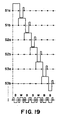
- Figures 16A - 16D illustrate pixel arrangements for color display.
- Figure 16A shows one pixel including three color pixels.
- Figures 16B - 16D illustrate three types of division of each color pixel (also called “dot") into sub-pixels (also called “sub-dot(s)").
- Each of Figures 16B - 16D illustrates a color pixel division allowing 16 gradation levels for each color pixel by division into two sub-pixels vertically and laterally.
- Figure 16B illustrates a simple division scheme similar to the one shown in Figure 15A.
- Figure 16C illustrates a half symmetrical arrangement scheme so as to alleviate the optical gravity center shift only in the vertical direction.
- Figure 16D illustrates a sub-pixel arrangement scheme capable of alleviating the optical gravity center shift in both the vertical and the lateral directions.
- Each scheme allows a display of 16 gradation levels (4 bits) for each color and totally 4096 colors (12 bits) for each pixel.
- a 12 bits/pixel display allows a display of 4096 colors; a 15 bits/pixel display, ca. 32000 colors; and a 24 bits/pixel display, ca. 16.8x10 6 colors.
- Other levels of color display are also possible, but an explanation hereinafter will be made based on the division scheme.
- standardized display modes requiring different numbers of pixels are present and may preferably be displayed on a single display panel.
- popular standardized display modes may include the following:
- the NTSC scheme as a standard home television scheme requires ca. 500 scanning lines, while the definition of the number of pixels is difficult by nature.
- a display panel e.g., a liquid crystal display panel
- the scanning electrodes (or scanning lines) are supplied with an electric signal (scanning signal) sequentially or in a time-sharing manner and, in synchronism therewith, the data electrodes (or data lines) are supplied with data signals to display a desired picture
- two scanning lines may be simultaneously selected to provide twice as fast a scanning speed. This is effective for providing an improved motion picture display quality and suppressing the flicker.
- Figure 17 schematically illustrates an example of pixel arrangement of a liquid crystal display panel and Figure 18 is a partially enlarged view thereof for illustrating one pixel arrangement.
- the liquid crystal display panel includes (laterally) 1280 x (vertically) 1024 pixels at intersections of stripe electrodes.
- Each pixel is divided in three primary color pixels (dots) of R, G and B.
- the R, G and B color pixels (dots) are each present in a number of 1280x1024.
- the scanning lines and data lines are respectively provided in non-uniform widths.
- the pixel division scheme is similar to the one shown in Figure 16C.
- each color pixel is composed of two data lines having a width ratio of 2:1, and three scanning lines having width ratios of 2:1:2, of which the upper and lower scanning lines are designed to be supplied with an identical electric signal by short-circuitry or logic treatment in the drive IC.
- Figure 18 is an enlarged view of one pixel in Figure 17, allowing display of 12 bits/pixel, i.e., 4096 colors/pixel.
- Figure 19 illustrates an example set of drive signal waveforms for effecting a high-resolution display according to an SXGA-mode of 1280x1024 on the panel of Figure 17.
- the scanning lines constituting the respective sub-pixels are driven line-by-line according to a basically non-interlaced mode.
- Each data line is supplied with a data signal of white (W) or black (B) so as to provide a desired display state.
- W white
- B black
- one-horizontal scanning period is denoted by 1H
- one picture rewriting period is 1H x (1024x2).
- the waveforms are according to the line clear-simultaneous writing scheme wherein (sub-)pixels on a preceding scanning line are cleaned simultaneously with writing in (sub-)pixels on a subsequent scanning line.
- the set of drive signals shown in Figure 19 is merely one example.
- the above-mentioned display panel may be driven at a higher speed by simultaneously driving a plurality of the scanning lines. For example, if two scanning lines each are driven simultaneously, one frame period will be reduced to 1Hx1024, i.e., twice as fast as the above not using simultaneous selection of two types of scanning lines.
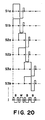
- An example set of drive signal waveforms according to this scheme is shown in Figure 20.
- two types of scanning lines a and b e.g., S1a and S1b
- this drive scheme may be referred to as an a-b/a-b simultaneous drive scheme, hereinafter.
- a conventional display device is accompanied with the following problem.
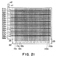
- Figure 21 shows an electrode or pixel arrangement of a display device disclosed in JP-A 7-270813 in which each pixel has a sub-pixel arrangement as shown in Figure 15B.
- All the scanning electrodes (S1a ... S8b 7) are disposed on one substrate 21 having a terminal side on which scanning electrode terminals S1a, S2a, S3a ... S8a each connecting two thick scanning electrodes and scanning electrode terminals S1b, S2b, S3b, ... S8b each connected to one narrow scanning electrode, are all disposed.
- all data electrodes (I1a ... I10b) are disposed on the other substrate 22, having a terminal side 23, on which data electrode terminals I1a, I2a, ... I10a each connecting two thick data electrodes and data electrode terminal I1b, I2b, ... I10b each connected to one narrow data electrode, are all disposed.
- Each device terminal electrical connection is similar to both of the devices shown in Figures 17 and 21 but, as for a physical electrode or wire connection, the one shown in Figure 21 is more common than the one shown in Figure 17, unless an expensive multi-layer electrode structure is adopted.
- Such a display device has to be equipped with a scanning electrode driver and a data electrode driver attached thereto.
- the terminal S1a and the terminal S1b for example have to be electrically isolated and independent from each other, so that their planar positions on the substrate 21 have to be separated from each other amply to some extent. Accordingly, the distances from the left edge of the substrate 21 to the respective terminals become different such that a distance (x1) to the terminal S1a is shorter than the distance (x2) to the terminal S1b.
- a driver comprising a dive circuit for the scanning electrodes or a drive circuit for the data electrodes is disposed along only one side of the substrate 21 or 22, a drive heat generated from the driver results in a temperature distribution along the display device, which is liable to adversely affect a device, of which the display performances are liable to be affected by a temperature change.
- An object of the present invention is to provide a driving method for a display device having a higher resolution display mode and a lower resolution mode while accomplishing improvements in both the display speed and the picture quality.
- Another object of the present invention is to provide a display device having pixels each comprising a plurality of sub-pixels, allowing easy connection with the drivers.
- a further object of the present invention is to provide a display device having pixels each comprising a plurality of sub-pixels, less liable to develop an undesirable temperature distribution.
- a driving method for a display device of the type comprising a plurality of scanning electrodes and a plurality of data electrodes so as to form a multiplicity of pixels each comprising a plurality of sub-pixels including a larger sub-pixel and a smaller sub-pixel having mutually different areas for displaying a plurality of gradation levels by application of an electric signal corresponding to given gradation data to each pixel, said driving method comprising applying a scanning selection signal to a plurality of scanning electrodes corresponding to at least two sub-pixels having an identical area of adjacent two pixels in an identical selection period.
- larger sub-pixels may be selected in a horizontal scanning period and smaller sub-pixels may be selected independently in another horizontal scanning period, so that the number of gradation levels or colors is not reduced in the lower resolution mode drive.
- the frequency of one frame for completing selection of all the scanning electrodes can be increased, thereby providing a display with little flicker or a good motion display.
- a display device comprising a plurality of pixels each comprising a plurality of sub-pixels including at least one sub-pixels corresponding to a first electrode and at least one other sub-pixel corresponding to a second electrode, wherein said first and second electrodes have their respective terminals which are disposed at one and the other of two mutually opposite edges of the display device.
- Figure 1 illustrates a set of drive signal waveforms used in an embodiment of the driving method according to the invention.
- Figure 2 is a partial plan view of a display device for illustrating an electrode arrangement used in the invention.
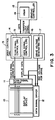
- Figure 3 is a block diagram of a display apparatus including a display device for practicing a driving method according to the invention.
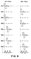
- Figures 4 - 9 are respectively a waveform diagram showing a set of time-serial drive signals according to an embodiment of the invention.
- Figure 10 is schematic plan view of a display device according to the invention showing an electrode arrangement and connection.
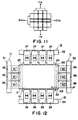
- Figure 11 illustrates an electrode arrangement for one pixel in a display device according to the invention.
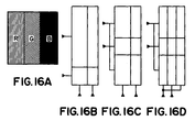
- Figure 12 is a schematic plan view for illustrating a manner of attaching drivers to a display device according to the invention.
- Figure 13 is a sectional view taken along a line A-A' in Figure 12.
- Figure 14 is a schematic plan view of a driver used in the invention.
- Figures 15A - 15C each show one unit pixel including a plurality of sub-pixels in a various pattern.
- Figures 16A - 16D each show one color pixel including a plurality of sub-pixels in a various pattern.
- Figure 17 is a partial plan view showing a pixel arrangement in a color display device.
- Figure 18 is a view showing one unit pixel of a color display device.
- Figures 19 and 20 are respectively a waveform diagram showing a set of time-serial drive signals used in a known driving method for a display device.
- Figure 21 is a schematic plan view showing a pixel arrangement shown in a known display device.
- Figure 1 is a waveform diagram showing a set of time-serially applied drive signal for principally illustrating a sequence of application of signals to the scanning electrodes, including a scanning selection signal comprising a pulse having a voltage V1 and a scanning non-selection signal having a voltage level Vref. Accordingly, a period for application of the pulse having a voltage V1 corresponds to a horizontal scanning period.
- data signals applied to a data electrode are shown.
- Figure 2 is a schematic partial plan view for illustrating an electrode arrangement and a pixel arrangement of a display device used in the present invention.
- S1a to S3b denote scanning electrodes and I1 to I3 denote data electrodes and, at intersections of these electrodes, larger sub-pixels PL1, PL2 and PL3 and smaller sub-pixels PS1, PS2 and PS3 are formed.
- Scanning electrodes corresponding to S4a and S4b and so on shown in Figure 1 are omitted from showing in Figure 2.
- scanning electrodes S1a and S2a corresponding to (or connected to) two larger pixels PL1 and PL2 are simultaneously supplied with a pulse having a voltage V1 as a scanning selection signal, and the other scanning electrodes are supplied with a voltage Vref as a scanning non-selection signal at that time.
- scanning electrodes S1b and S2b corresponding to (or connected to) smaller pixels PS1 and PS2 are simultaneously supplied with a pulse having a voltage V1 to be selected simultaneously.
- the larger pixels PL1 and PL2 are placed in an identical display state (optical state), and the smaller pixels PS1 and PS2 are placed in an identical display state independent from that of the large pixels PL1 and PL2.
- a unit pixel as a gradational display unit is composed of 4 sub-pixels PL1, PS1, PL2 and PS2.
- This is a low-resolution and high-speed first display mode.
- the scanning electrodes may be sequentially selected in the order of S1a, S1b, S2a, S2b, S3a, S3b, ... in a non-interlaced mode, or sequentially selected in the order of S1a, S2a, S3a, ...
- a unit pixel as a gradational display unit is composed of two sub-pixels, i.e., larger sub-pixel PL1 and a smaller sub-pixel PS1, so that a high-resolution display is effected.
- Figure 3 is a block diagram of a display apparatus according to the present invention including a display device 10, a scanning signal driver 11 for applying a scanning selection signal or a scanning non-selection signal selectively to the scanning electrodes, and a data signal driver 12 for applying data signals for determining the display states of the pixels to the data electrodes,
- the display apparatus further includes a control circuit 13 which in turn includes a drive control circuit 14 and a drive voltage generation circuit 17.
- the drive control circuit 14 includes a scanning signal control circuit 15 which supplies the scanning signal driver 11 with scanning signal address data including data for determining the order of selection of the scanning electrodes. The data is determined depending on the display mode, whereby the scanning electrodes are scanned (i.e., selected) sequentially in the above-described manner by the driver 11.
- the dive control circuit 14 further includes a data signal control circuit 16 for supplying the driver 12 with display data corresponding to the scanning signal address data.
- the drivers 11 and 12 receive reference voltages (e.g., V1, Vref, V2 and V3) for drive from the drive voltage generation circuit 17 and supply drive signals as shown in Figure 11 determined based on combinations of the reference voltages for prescribed durations by means of switching elements (not shown) to the scanning electrodes and the data electrodes.
- reference voltages e.g., V1, Vref, V2 and V3
- the display apparatus further includes a graphic controller 18 for storing video data including gradation data in a VRAM 19 and supplies the video data read from the VRAM 19 together with transfer clock signals to the control circuit 13.
- a graphic controller 18 for storing video data including gradation data in a VRAM 19 and supplies the video data read from the VRAM 19 together with transfer clock signals to the control circuit 13.
- multi-value gradation data for each pixel may be converted into binary data for each sub-pixel (so as to provide a multi-value for a pixel concerned) by the graphic controller.
- the display device 10 for monochromatic or color display used in the present invention may comprise, e.g., an electroluminescence device, an electrochromic device, a liquid crystal device, an electron discharge device, a plasma device or a micro-mirror device.
- a liquid crystal device may be particularly preferably used.
- the liquid crystal material used may preferably comprise a chiral smectic liquid crystal or nematic liquid crystal.
- a chiral smectic liquid crystal is known to form a ferroelectric or anti-ferroelectric liquid crystal exhibiting a memory characteristic for a long hour and is desirably used for providing a high-resolution display.
- a chiral nematic liquid crystal exhibiting a memory characteristic for a relatively short time may also be preferably used.
- the scanning electrodes and data electrodes may be arranged to constitute either a simple matrix-type or an active matrix type device structure.
- one electrode may be composed by a partially superposed combination of a high-resistivity transparent electrode and a low-resistivity opaque conductor, and the areal size of each sub-pixel is determined depending on the exposed area of the transparent electrode pattern.
- sub-pixel arrangement pattern may be similar to one shown in any of Figures 15A, 15B, 16B, 16C and 16D.
- Drive signals applied to the scanning electrodes and data electrodes may be appropriately determined depending on a display medium constituting pixels and need not be restricted to those shown in Figure 1. Some examples thereof will be described in more detail with reference to embodiments described hereinafter. Further, scanning selection signals applied to scanning electrodes (e.g., S1a and S2a in Figure 1), which are horizontally scanned simultaneously, need not comprise pulses which rise and fall completely simultaneously with each other as shown in Figure 1, if two scanning electrodes are substantially simultaneously selected to determine display states.
- Figure 1 shows an embodiment, wherein two unit pixels in a high-resolution mode display constitute one unit pixel in a low-resolution mode display. However, in case where a low-resolution mode display is performed three or four or more unit pixels, three or four or more scanning electrodes are simultaneously selected.
- a prescribed number (N) of scanning electrodes are preferentially scanned among totally M scanning electrodes (M>N).
- M>N a prescribed number of scanning electrodes
- “preferential scanning” means that the prescribed number of scanning electrodes are scanned or selected at a higher frequency than the other scanning electrodes.
- the preferential scanning may preferably be applied to a partial rewrite display mode, which may be used to display a good quality of motion picture in a window defined in a whole picture area. Further, the sticking of a background picture may also be suppressed.
- FIG. 4 shows a set of drive signal waveforms for a scanning sequence, whereby two "a"-scanning lines (wider scanning lines) are simultaneously scanned (referred to as “a-a simultaneous drive”), and then two "b"-scanning lines (narrower scanning lines) are simultaneously scanned (referred to as "b-b simultaneous drive”) for two pixels each.
- one frame (whole picture) scanning period is reduced to a half, thereby providing an increased scanning speed.
- the number of colors displayable by 2x2 pixels, each having a sub-pixel arrangement pattern as shown in Figure 18, may be calculated as follows.
- the a-a/b-b simultaneous drive according to this embodiment provides an increased number of displayable colors (of more than ten times).
- one frame operation is completed by four fields of vertical scanning.
- a high-quality picture with less flicker and smooth motion picture can be displayed even at a low frame frequency.
- a good picture quality can also be displayed by changing the order of the respective fields.
- Example 2 This example adopts a different order of field selection from that in Example 2 as follows:
- one frame operation is performed in 6 fields by scanning the scanning electrodes with scanning.
- a high-quality picture with less flicker and smooth motion picture can be displayed even at a low frame frequency.
- a good picture quality can also be displayed by changing the order of the respective fields.
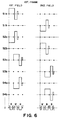
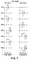
- This example adopts a set of drive waveforms (shown in Figures 6 and 7) by replacing a portion of the drive waveforms used in Example 2 (shown in Figure 5).
- Figure 6 shows a first frame
- Figure 7 shows a second frame.
- scanning signals having mutually polarity-inverted waveforms are applied to simultaneously selected scanning electrodes, e.g., S1a and S2a.
- mutually polarity-inverted scanning signals are simultaneously applied to the scanning electrodes each for selection of the other scanning electrodes.
- a different order of mutually polarity-inverted scanning signals are sequentially applied to two scanning electrodes each, i.e., S1b - S2b, S3b - S4b, ...
- two scanning electrodes each are again sequentially selected so that each scanning electrode receives a polarity-inverted scanning signal to effect a frame inversion drive scheme.
- the drive margin is improved so that a liquid crystal panel can be produced at a high productivity while ensuring a good picture quality.
- a liquid crystal device was prepared by using a chiral nematic liquid crystal exhibiting bistability. Details of the operation principle of this type of liquid crystal device are disclosed in, e.g., EP-A 569,029 (corresponding to JP-A 6-230751.
- the liquid crystal material used was prepared by mixing a chiral dopant ("S811", available from Merck Co.) with a commercially available liquid crystal material ("KN-4000", available from Chisso K.K.) so as to provide a helical pitch of 3.6 ⁇ m.
- the device was prepared by providing a pair of electrode plates with a rubbed 100 nm-polyimide alignment film and assembling the electrode plates so that their rubbing directions were parallel and opposite to each other and the cell gap became 2 ⁇ m.
- the liquid crystal device could be driven for writing under conditions including reset pulse voltages of ⁇ 20 volts, writing voltages of ⁇ 2.5 volts, data signal voltage of ⁇ 1.5 volts and one-line writing time of 300 ⁇ sec.
- the liquid crystal device was driven by switching between a high resolution mode wherein all the scanning lines were independently scanned, and the above-mentioned a-a/b-b simultaneous drive mode, whereby display at respective resolutions could be attained.
- a high-resolution display may be performed on the whole or a part of the picture area by scanning all the scanning electrode in the related area according to the above-mentioned non-interlaced or interlaced scanning scheme.
- Example 8 is modified by including an additional display mode wherein a partial rewrite scanning is performed by selecting only scanning electrodes S1a, S2a, S3a, S4a ... corresponding to larger-area sub-pixels and not selecting scanning electrodes S1b, S2b ...
- all the scanning electrodes are selected according to the non-interlaced or interlaced scanning scheme to effect a display of 16 gradation levels for each color and totally 4096 colors for each pixel.
- a second display mode for a high-speed display at a low resolution the set of drive signals shown in Figure 4 (used in Example 1) are used to display 31 gradation levels for each color and 29791 colors for 2x2 pixels.
- This second display mode is suitable for a motion picture display.
- a third display mode the above-mentioned additional display mode is adopted to perform a partial rewrite operation while attaching a greater importance to a high-speed operation.
- a low-resolution display with little flicker and suitable for motion picture display can be performed without decreasing the number of displayable gradation levels or colors.
- Figure 10 illustrates a display device according to another embodiment of the present invention.
- a substrate 21 is provided with all the scanning electrodes, odd-numbered a terminals S1a, S3a, S5a, S7a ... each short-circuiting two scanning electrodes are disposed on a left-side terminal region 25, and even-numbered a terminals S2a, S4a, S5a, S8a ... each also short-circuiting the scanning electrodes are disposed on a right-side terminal region 26.
- a group of scanning electrodes each disposed between the short-circuitted two electrodes are extended to provide terminals S2b, S4b, S6b, S8b ... which are disposed on the left-side terminal region 25, and the remaining group of scanning electrodes each disposed between the short-circuited two electrodes are extended to provide terminals S1b, S3b, S5b, S7b ... which are disposed on the right-side terminal region 26.
- a substrate 22 is provided with all data electrodes.
- terminals I1a, I3a, i5a, I7a, I9a ... are disposed on an upper terminal region 24, and terminals I2a, I4a, I6a, I8a, I10a ... are disposed on a lower terminal region 23.
- terminals I2b, I4b, I6b, I8b, I10b ... are disposed on the upper terminals region 24, and terminals I1b, I3b, I5b, I9b, I9b ... are disposed on the lower terminal region.
- each terminal is depicted in a narrower width than each electrode for easy comprehension of the arrangement, but the terminals actually have a larger width than the electrode in many cases where the terminals are disposed at a much higher density than that supposed from Figure 10.
- the above-mentioned arrangement may be simplified for one pixel arrangement as shown in Figure 11, so that a terminal S1a for short-circuitted two scanning electrodes (first electrodes) and a terminal for one scanning electrode disposed between the two scanning electrodes may be regarded as being disposed on mutually opposite left and right edges, respectively, of one substrate.
- a terminal I1a for short-circuitted two data electrodes (first electrodes) and a terminal I1b for one data electrode disposed between the two data electrodes may be regarded as being disposed on mutually opposite upper and lower edges of one substrate.
- Figure 12 is a plan view for illustrating a peripheral arrangement of scanning electrode drivers 11 and data electrode drivers 12 attached to a display device 10 having a similar structure as the one shown in Figure 10.
- the scanning electrode drivers 11 include flexible films 35 and 36 mounted with IC chips 41 and 42, respectively, for driving the scanning electrodes
- the data electrode drivers 12 include flexible films 37 and 38 mounted with IC chips 43 and 44, respectively, for driving the data electrodes.
- These flexible films are generally called TCPs (tape carrier packages) according to the TAB (tape-automated bonding) method.
- TCPs 35 and 36 ar connected to circuit boards 31 and 32, respectively, for transmitting address signals and signals for controlling the operation of the IC chips 41 and 42.
- TCPs 37 and 38 are connected to circuit boards 33 and 34, respectively, for transmitting picture data and signals for controlling the operation of the IC chips 43 and 44.
- a TCP 36 for example, comprises a flexible film 49 comprising a resin such as polyimide and provided with conductor patterns 47 and 48, each comprising an electroconductive material, such as copper. Also an IC chip 42 is mounted on the film 49, and terminals of the IC chip 42 are connected with the conductor patterns 47 and 48. Further, the connecting parts are covered with a sealing material 50, such as silicon resin.
- the conductor pattern 47 forms output terminals for supplying drive signals, which are connected to scanning electrode terminals on the substrate 21 with a connecting member 46, such as an anisotropic conductor film.
- the conductor pattern 48 forms input terminals for the IC chip 47, which are connected to terminals of the print circuit board 32 with a connecting member 45, such as an anisotropic conductor film or solder.
- Figure 14 is a schematic plan view of a TCP including one IC chip.
- the patterned conductors 47 and 48 as the terminals are respectively arranged along two sides of the flexible film 49.
- the arrangement shown in Figure 10 of terminals having an identical distance to a substrate edge allows a simpler positional alignment and a simpler pattern of conductors 47, thus being economically advantageous. Further, it is practically impossible to realize a terminal arrangement pattern as shown in Figure 17 unless a multi-layer conductor disposition pattern including a disposition of an intermediate insulating layer is adopted.
- connection failures such as a short circuit and the opening of a connection.
- the drivers are attached to both upper and lower edges and/or both left and right edges of the display device 10.
- the terminal arrangement according to the present invention is adopted for both the scanning electrodes and the data electrodes.
- the terminal arrangement according to the present invention may be applied to only the scanning electrodes.
- the terminals S1a and S2b are disposed on one side, and the terminals S1b and S2a are disposed on the other opposite side. This is for equalizing the loads on both sides of IC chips for driving the electrodes.
- terminals S1a, S2a, S3a ... S8a may be disposed on one side and terminals S1b, S2b, S3b, .. S8b may be disposed on the other side as another embodiment, but the embodiment of Figure 10 is preferred to such another embodiment.
- the display device of Figure 10 may be suitably driven by using, a set of scanning signal waveforms and data signal waveforms, e.g., as shown in Figure 4.
- a scanning selection signal is simultaneously applied to scanning electrode terminals S1a and S2a.
- the scanning selection signal includes a pulse of one polarity for simultaneously clearing (or erasing or resetting) sub-pixels on a selected scanning electrode, a writing pulse of the other polarity and a small pulse of one polarity for preventing crosstalk.
- the other terminals are supplied with a reference voltage as a scanning non-selection signal.
- scanning electrode terminals S1b and S2b are simultaneously supplied with a scanning selection signal to determine display states of sub-pixels on the selected scanning electrodes.
- data electrode terminals (I1a, I1b, I2a, I2b, .. I10a, I10b ”) are supplied with data signals I (including a B signal for providing a dark display state and a W signal for providing a bright display state).
- the display states of two pixels each disposed along a direction of extension of data electrodes are determined.
- the display device 10 is supplied with scanning selection signals and data signals always from the drivers disposed on four sides including the upper and lower sides and the left and right sides, only a reduced temperature difference can be developed at any points over the display device 10. As a result, even a device having a temperature-dependence of display performance can be driven to provide an equally good display state similarly as a device having little temperature-dependence of display performance.
- the drive waveform shown in Figure 4 is suitable for effecting a high-speed display at a number of pixels which is smaller than the number of pixels potentially displayable by the device.
- the display device shown in Figure 10 has 1280x1024 pixels
- mutually adjacent 2x2 pixels may be driven corresponding to one pixel in order to display a VGA picture comprising 640x480 pixels.
- a VGA picture can be displayed in an enlarged size by using 1280x960 pixels of the display device.
- one frame scanning period may be divided into at least two field scanning periods, so that scanning electrode terminals S1a, S2a, S3a ... S8a are sequentially supplied with a scanning selection signal in a first field, and scanning electrode terminals S1b, S2b, S3b ... S8b are sequentially supplied with a scanning selection signal, while supplying data signals to the data electrode terminals in synchronism with the application of the scanning selection signals.
- the complication of terminal arrangement pattern for the scanning electrodes and/or the data electrode can be prevented to allow an easy connection with the drivers. Further, as the drivers are connected to both sides of a display device, it is possible to obviate a temperature increase along one side of the device due to heat generation disposed thereat, so that it is possible to effect good operation of even a display device having temperature-depending display performances.
- a display device includes a plurality of scanning electrodes and a plurality of data electrodes so as to form a multiplicity of pixels each comprising a plurality of sub-pixels having mutually different areas for displaying a plurality of gradation levels by application of an electric signal corresponding to given gradation data to each pixel.
- the display device is driven by applying a scanning selection signal to a plurality of scanning electrodes corresponding to at least two sub-pixels having an identical area of adjacent two pixels in an identical selection period.
- a display device may be formed such that each pixel includes at least one sub-pixel corresponding to a first electrode and at least one other sub-pixel corresponding to a second electrode, wherein said first and second electrodes have their respective terminals which are disposed at one and the other of two mutually opposite edges of the display device.
Abstract
Description
said driving method comprising applying a scanning selection signal to a plurality of scanning electrodes corresponding to at least two sub-pixels having an identical area of adjacent two pixels in an identical selection period.


Claims (20)
- A driving method for a display device of the type comprising a plurality of scanning electrodes and a plurality of data electrodes so as to form a multiplicity of pixels each comprising a plurality of sub-pixels including a larger sub-pixel and a smaller sub-pixel having mutually different areas for displaying a plurality of gradation levels by application of an electric signal corresponding to given gradation data to each pixel,
said driving method comprising applying a scanning selection signal to a plurality of scanning electrodes corresponding to at least two sub-pixels having an identical area of adjacent two pixels in an identical selection period. - A driving method according to Claim 1, wherein scanning electrodes corresponding to a region including pixels for which picture data has changed among said multiplicity of pixels are preferentially selected for rewriting the region.
- A driving method according to Claim 1, comprising a mode of operation wherein one picture is formed by at least two vertical scanning periods including one vertical scanning period wherein only scanning electrodes corresponding to the larger sub-pixels are vertically scanned.
- A driving method according to Claim 1, wherein a frame operation for selecting all the scanning electrodes is divided into a plurality of vertical scanning fields so that all the scanning electrodes are divided into a plurality of groups each including a plurality of scanning electrodes receiving a scanning selection signal in an identical selection period and, in each vertical scanning field, the plurality of groups of scanning electrodes are selected sequentially while skipping at least one group of scanning electrodes for each selection.
- A driving method according to Claim 1, wherein said plurality of sub-pixels of each pixel include a smallest-area sub-pixel and at least one pair of sub-pixels disposed at symmetrical positions with respect to the smallest-area sub-pixel.
- A driving method according to Claim 1, wherein each pixel includes a display medium assuming two optical states.
- A driving method according to any one of Claims 1 - 6, wherein each pixel includes a display medium comprising a chiral smectic liquid crystal.
- A driving method according to any one of Claims 1 - 6, wherein each pixel includes a display medium comprising a nematic liquid crystal.
- A driving method according to any one of Claims 1 - 6, comprising a plurality of operation modes using different numbers of or different sizes of pixels.
- A display apparatus, including:a display device comprising a plurality of scanning electrodes and a plurality of data electrodes so as to form a multiplicity of pixels each comprising a plurality of sub-pixels having mutually different areas, anddrive means for applying electrical signals to the respective sub-pixels depending on given gradation data;
said drive means including a scanning electrode drive circuit for applying a scanning selection signal to a plurality of scanning electrodes corresponding to at least two sub-pixels having an identical area of adjacent two pixels in an identical selection period. - A display device, comprising a plurality of pixels each comprising a plurality of sub-pixels including at least one sub-pixels corresponding to a first electrode and at least one other sub-pixel corresponding to a second electrode, wherein said first and second electrodes have their respective terminals which are disposed at one and the other of two mutually opposite edges of the display device.
- A display device according to Claim 11, wherein said first and second electrodes are scanning electrodes.
- A display device according to Claim 11, wherein said first and second electrodes are data electrodes.
- A display device according to Claim 11, wherein each pixel includes a pair of sub-pixels corresponding to the first electrode and a sub-pixel disposed between the pair of sub-pixels corresponding to the second electrode.
- A display device according to Claim 11, wherein two adjacent pixels are disposed such that the first electrode for one pixel and the first electrode for the other pixel have terminals disposed at the mutually opposite edges of the display device.
- A display device according to Claim 11, wherein two adjacent pixels are disposed such that each pixel includes a sub-pixel corresponding to the second electrode disposed between a pair of sub-pixels corresponding to the first electrode,the terminal for the first electrode for one pixel and the terminal for the second electrode for the other pixel are disposed at one edge of the display device, andthe terminal for the second electrode for said one pixel and the terminal for the first electrode for said the other pixel are disposed at another edge opposite to said one edge of the display device.
- A display device according to Claim 11, wherein a flexible film carrying an IC chip is attached to each of said mutually opposite two edges of the display device.
- A driving method for a display device according to Claim 11, wherein each pixel comprises a plurality of sub-pixels having mutually different areas for displaying a plurality of gradation levels by application of an electric signal corresponding to given gradation data to each pixel,
said driving method comprising applying a scanning selection signal to a plurality of scanning electrodes corresponding to at least two sub-pixels having an identical area of adjacent two pixels in an identical selection period. - A driving method according to Claim 18, wherein said plurality of sub-pixels of each pixel include a smallest-area sub-pixel and at least one pair of sub-pixels disposed at symmetrical positions with respect to the smallest-area sub-pixel.
- A driving method according to Claim 18, wherein each pixel includes a display medium assuming two optical states.
Applications Claiming Priority (4)
| Application Number | Priority Date | Filing Date | Title |
|---|---|---|---|
| JP26838196A JPH10115820A (en) | 1996-10-09 | 1996-10-09 | Driving method for display element, and display device |
| JP268381/96 | 1996-10-09 | ||
| JP24398897A JPH1184407A (en) | 1997-09-09 | 1997-09-09 | Display element |
| JP243988/97 | 1997-09-09 |
Publications (2)
| Publication Number | Publication Date |
|---|---|
| EP0836172A2 true EP0836172A2 (en) | 1998-04-15 |
| EP0836172A3 EP0836172A3 (en) | 1999-01-07 |
Family
ID=26536524
Family Applications (1)
| Application Number | Title | Priority Date | Filing Date |
|---|---|---|---|
| EP97117385A Withdrawn EP0836172A3 (en) | 1996-10-09 | 1997-10-08 | Display device using sub-pixels and driving method therefor |
Country Status (1)
| Country | Link |
|---|---|
| EP (1) | EP0836172A3 (en) |
Citations (6)
| Publication number | Priority date | Publication date | Assignee | Title |
|---|---|---|---|---|
| EP0453033A1 (en) * | 1990-04-20 | 1991-10-23 | Koninklijke Philips Electronics N.V. | Display device |
| EP0471460A2 (en) * | 1990-08-16 | 1992-02-19 | International Business Machines Corporation | Liquid crystal display device |
| EP0673012A2 (en) * | 1994-03-11 | 1995-09-20 | Canon Information Systems Research Australia Pty Ltd. | Controller for a display with multiple common lines for each pixel |
| EP0685832A1 (en) * | 1994-06-01 | 1995-12-06 | Sharp Kabushiki Kaisha | A ferroelectric liquid crystal display device and a driving method of effecting gradational display thereof |
| EP0703561A2 (en) * | 1994-09-26 | 1996-03-27 | Canon Kabushiki Kaisha | Driving method for display device and display apparatus |
| EP0717390A2 (en) * | 1994-12-14 | 1996-06-19 | Canon Kabushiki Kaisha | Display device with a reference potential wiring |
-
1997
- 1997-10-08 EP EP97117385A patent/EP0836172A3/en not_active Withdrawn
Patent Citations (6)
| Publication number | Priority date | Publication date | Assignee | Title |
|---|---|---|---|---|
| EP0453033A1 (en) * | 1990-04-20 | 1991-10-23 | Koninklijke Philips Electronics N.V. | Display device |
| EP0471460A2 (en) * | 1990-08-16 | 1992-02-19 | International Business Machines Corporation | Liquid crystal display device |
| EP0673012A2 (en) * | 1994-03-11 | 1995-09-20 | Canon Information Systems Research Australia Pty Ltd. | Controller for a display with multiple common lines for each pixel |
| EP0685832A1 (en) * | 1994-06-01 | 1995-12-06 | Sharp Kabushiki Kaisha | A ferroelectric liquid crystal display device and a driving method of effecting gradational display thereof |
| EP0703561A2 (en) * | 1994-09-26 | 1996-03-27 | Canon Kabushiki Kaisha | Driving method for display device and display apparatus |
| EP0717390A2 (en) * | 1994-12-14 | 1996-06-19 | Canon Kabushiki Kaisha | Display device with a reference potential wiring |
Non-Patent Citations (1)
| Title |
|---|
| TSUGUJI TACHIUCHI ET AL.: "A Color LCD Controller" IEEE TRANSACTIONS ON CONSUMER ELECTRONICS, vol. ce-33, no. 3, August 1987, pages 359-365, XP002082590 * |
Also Published As
| Publication number | Publication date |
|---|---|
| EP0836172A3 (en) | 1999-01-07 |
Similar Documents
| Publication | Publication Date | Title |
|---|---|---|
| KR100408350B1 (en) | Method for driving display, driving circuit therefor, display, and electronic apparatus | |
| JP3560756B2 (en) | Driving method of display device | |
| KR0171938B1 (en) | Liquid crystal display device | |
| KR100232983B1 (en) | Display panel and apparatus capable of resolution conversion | |
| US6225967B1 (en) | Matrix-driven display apparatus and a method for driving the same | |
| JP3039404B2 (en) | Active matrix type liquid crystal display | |
| US5808594A (en) | Driving method for display device and display apparatus | |
| US8330700B2 (en) | Driving circuit and driving method of active matrix display device, and active matrix display device | |
| JP3264248B2 (en) | Active matrix type liquid crystal display | |
| JPH04502520A (en) | Flicker-free LCD display driver device | |
| US6147792A (en) | Light modulating devices | |
| US20080158125A1 (en) | Liquid crystal display device | |
| JP3426723B2 (en) | Liquid crystal display device and driving method thereof | |
| JP2004355017A (en) | Liquid crystal display device and its driving method | |
| KR100258169B1 (en) | Liquid crystal apparatus using different types of drive waveforms alternately | |
| US7283113B2 (en) | Method and apparatus for driving liquid crystal display | |
| EP0836172A2 (en) | Display device using sub-pixels and driving method therefor | |
| US6028579A (en) | Driving method for liquid crystal devices | |
| JP3896874B2 (en) | Driving method of electro-optic element | |
| JP4050383B2 (en) | Liquid crystal display device driving method, liquid crystal display device, and electronic apparatus | |
| JP3658952B2 (en) | Liquid crystal display device drive voltage adjustment method, liquid crystal display panel drive device, liquid crystal display device, liquid crystal display device drive voltage adjustment device, and electronic apparatus | |
| JPH08136892A (en) | Liquid crystal display device | |
| JPH11133918A (en) | Drive for liquid crystal display panel, liquid crystal display, and electronic appliance | |
| JP3415965B2 (en) | Driving method of image display device | |
| KR20030004872A (en) | Liquid Crystal Display and Driving Method and Apparatus Thereof |
Legal Events
| Date | Code | Title | Description |
|---|---|---|---|
| PUAI | Public reference made under article 153(3) epc to a published international application that has entered the european phase |
Free format text: ORIGINAL CODE: 0009012 |
|
| 17P | Request for examination filed |
Effective date: 19971008 |
|
| AK | Designated contracting states |
Kind code of ref document: A2 Designated state(s): DE FR GB |
|
| AX | Request for extension of the european patent |
Free format text: AL;LT;LV;RO;SI |
|
| PUAL | Search report despatched |
Free format text: ORIGINAL CODE: 0009013 |
|
| AK | Designated contracting states |
Kind code of ref document: A3 Designated state(s): AT BE CH DE DK ES FI FR GB GR IE IT LI LU MC NL PT SE |
|
| AX | Request for extension of the european patent |
Free format text: AL;LT;LV;RO;SI |
|
| AKX | Designation fees paid |
Free format text: DE FR GB |
|
| STAA | Information on the status of an ep patent application or granted ep patent |
Free format text: STATUS: THE APPLICATION IS DEEMED TO BE WITHDRAWN |
|
| 18D | Application deemed to be withdrawn |
Effective date: 20051119 |