EP0829914A2 - Filtering arrangement with impedance step resonators - Google Patents
Filtering arrangement with impedance step resonators Download PDFInfo
- Publication number
- EP0829914A2 EP0829914A2 EP97307041A EP97307041A EP0829914A2 EP 0829914 A2 EP0829914 A2 EP 0829914A2 EP 97307041 A EP97307041 A EP 97307041A EP 97307041 A EP97307041 A EP 97307041A EP 0829914 A2 EP0829914 A2 EP 0829914A2
- Authority
- EP
- European Patent Office
- Prior art keywords
- frequency
- section
- filter
- radio
- band
- Prior art date
- Legal status (The legal status is an assumption and is not a legal conclusion. Google has not performed a legal analysis and makes no representation as to the accuracy of the status listed.)
- Granted
Links
Images


Classifications
-
- H—ELECTRICITY
- H01—ELECTRIC ELEMENTS
- H01P—WAVEGUIDES; RESONATORS, LINES, OR OTHER DEVICES OF THE WAVEGUIDE TYPE
- H01P1/00—Auxiliary devices
- H01P1/20—Frequency-selective devices, e.g. filters
- H01P1/201—Filters for transverse electromagnetic waves
- H01P1/205—Comb or interdigital filters; Cascaded coaxial cavities
- H01P1/2056—Comb filters or interdigital filters with metallised resonator holes in a dielectric block
Definitions
- the invention relates to radio-frequency filters which, due to their construction, have multiple simultaneous operating frequencies.
- Filters based on transmission line resonators are fundamental components in modern radio apparatuses. Categorized according to the frequency response, the commonest filter types are band rejection and band pass filters which are used to attenuate high-frequency signals on a desired frequency band (band rejection) or outside a certain frequency band (band pass). In addition, low pass and high pass filters are used.
- Transmission line resonators the resonating frequencies of which determine a filter's frequency response, are usually cylindrical coil conductors, or helixes, plated grooves or holes formed in a dielectric medium, coaxial outer/inner conductor pairs or strip lines formed on a board-like substrate. There are usually from two to about eight resonators in a filter.
- a filter is connected to the rest of the radio apparatus via input, output and control signal ports.
- GSM Global System for Mobile Telecommunications
- JDC Japanese Digital Cellular
- PCN Personal Communication Network
- PCS Personal Communication System
- the operating frequencies of the American AMPS mobile phone system are 824-894 MHz and those of the European cordless telephone system, DECT, 1880-1900 MHz.
- GSM and DECT Digital European Cordless Telephone
- GSM and PCN Personal Communication Network
- the dual mode capability is also taken into account in the so-called third generation cellular systems (Universal Mobile Telecommunication System, UMTS/ Future Public Land Mobile Telecommunications System, FLPMTS).
- the filtering arrangement can be realized in two ways.
- the filters In the first solution, the filters must meet the same requirements at both frequencies.
- the band pass filter must have a pass band at the both operating frequencies of the system, the band rejection filter must have corresponding stop bands and so forth.
- radio signals of different frequencies are directed via different routes, in which case the apparatus has got two parallel filters for each filtering function.
- the first solution is more advantageous in apparatuses where minimization of physical size is important.
- Figure 2 shows a typical frequency response for the filter.
- the filter's first pass band is at the frequency f0 and the next pass band, determined by the resonators' first odd harmonic resonating frequency fs1, is at the frequency 3*f0.
- the harmonic frequency is too high to be used for dual band/dual mode filtering.
- An object of this invention is to provide a filtering arrangement wherein the filtering parts of a radio apparatus operating at two operating frequencies can employ at least partly shared resonators.
- This object of the invention can be achieved by using in the filters of a radio apparatus impedance step resonators the specifications of which are chosen such that they operate at the desired frequencies.
- the filtering arrangement according to the invention is characterized in that the fundamental resonating frequency of the impedance step resonators is on the first frequency band of a dual band radio system and a certain harmonic resonating frequency is on the second frequency band of the radio system.
- the invention is based on the perception that the harmonic resonating frequency of a transmission line resonator can be shifted down from the relatively high value mentioned above to a desired second operating frequency band using a so-called impedance step construction.
- the idea of changing the impedance of a resonator in the direction of its longitudinal axis is known, but the resulting shift in the resonating frequency has been regarded as only a means to attenuate harmonic frequencies or to influence the inter-resonator electromagnetic coupling in the filters of a radio apparatus designed for one frequency band.
- the dimensioning of the impedance step resonator or resonators shifts the chosen harmonic resonating frequency in such a way that the fundamental frequency of the resonator or resonators produces for a filter consisting of the resonators a desired frequency response in the first operating frequency range and the harmonic frequency produces a corresponding frequency response for the filter in the second operating frequency range.
- an impedance step resonator In addition to constant-impedance ⁇ /4 transmission line resonators, an impedance step resonator, schematically depicted in Figure 3, is employed by certain filters designed for mobile phone applications.
- the ⁇ /4 resonator in the figure comprises two consecutive transmission lines TL1 and TL2, and the impedances of its open and short-circuited ends are unequal.
- the use of impedance step resonators aims at shortening the physical length of the resonator construction and/or improving the harmonic attenuation characteristics of the filter.
- 4 506 241 discloses how a first odd harmonic resonating frequency (fs1) can be shifted further up from frequency 3*f0 so that the harmonic attenuation requirements of a filter in a system in the frequency range f0 can be met.
- the construction is also used in a filter where one dielectric block comprises several resonators.
- US Patent No. 4 733 208 discloses how the impedance step construction is applied to the adjustment of electromagnetic coupling between such resonators.
- the impedance step resonator has such specifications that its fundamental resonating frequency, marked f0 below, is at the lower operating frequency of the dual band or dual mode apparatus and the odd harmonic resonating frequency (fs1) is at the higher operating frequency of the apparatus. Then that resonator can be used for filtering in both systems.
- Figure 4 is a longitudinal section of a known implementation of the impedance step resonator.
- a dielectric body block 1 is bounded by two parallel end surfaces 3 and 4, which customarily are called an upper surface (3) and a lower surface (4) without any restrictions to the operating position of the construction.
- the block is further bounded by side surfaces 2, which are perpendicular to the end surfaces and most often parallel in pairs, thereby making the block 1 a rectangular prism.
- the block has a cylindrical hole for a resonator, and a first section 5 of the hole has a diameter greater than that of a second section 6.
- the length of section 5 is denoted by L1 and the length of section 6 by L2.
- the inner surfaces of the holes 5, 6 and at least part of the lower surface 4 are coated with an electrically conductive material.
- the resonator hole 6 opening to the upper surface 3 is disconnected from the coating, either so that the entire upper surface 3 is uncoated or so that there is an electrically non-conductive area around the hole. It is also possible to form the resonator hole so that it does not open to the upper surface such that the resonator hole is closed on the side of the upper surface 3.
- the coating on the lower surface 4 is formed in such a manner that it is connected to the resonator hole coating and hence to the side surface coating, thereby forming a short-circuited end for the resonator.
- the impedance step is formed by making a step in the resonator hole in such a manner that the diameter of the hole facing the filter's upper surface 3 is smaller than that of the hole facing the lower surface 4.
- the holes with different diameters have different impedances.
- the impedance of the hole 5 facing the short-circuited end is smaller than that of the hole 6 facing the open end.
- the resonator is physically a little longer in the horizontal direction of the drawing than a constant-impedance transmission line resonator.
- the invention is not limited to a dielectric resonator arrangement like the one described above but it can be applied in many ways.
- Impedance step resonators can also be strip line resonators, for example.
- the impedance step need not necessarily be achieved by means of a step in the inner conductor but the step may also be located on the plated outer surface of the body block.
- formula (3) gives us the length of the resonator parts 5 and 6 which only depends on the frequency f0.
- the same formulas apply to any ratio of the frequencies f0 and fs1.
- Substituting the desired frequency values in formula (2) we get a value for K which together with frequency f0 determines the length of the resonator parts according to formula (3).
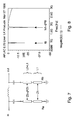
- Figure 6 shows the simulated frequency response of such a filter.
- the filter has two obvious pass bands the first of which is at frequency f0 and the second is at a frequency two times higher.
- Figure 8 shows the simulated frequency response of such a filter. We can see that the filter has two obvious stop bands the first of which is at frequency f0 and the second is at a frequency two times higher.
- Figure 9 shows a filter according to an advanced embodiment of the invention, where the basic element is a filter according to Figure 5.
- the port (in) depicted as an input port in Figure 5 is an antenna port (port 1) in the filter shown in Figure 9. From an output port (out) according to Figure 5 the signal path branches into a lower frequency band branch (port 2) and higher frequency band branch (port 3).
- LC circuit LC1 comprising an inductive and a capacitive element connected in parallel, which attenuates signals propagating at frequency 2*f0.
- LC high pass chain LC2 according to a known construction to provide sufficient attenuation in this branch at frequency f0 and to provide the necessary isolation between ports 2 and 3.
- Figure 10 illustrates simulated pass attenuation between ports 1 and 2 for a filter according to Figure 9, and Figure 11 illustrates simulated pass attenuation between ports 1 and 3 for the same filter.
- the filter has between ports 1 and 2 a pass band at f0 and a narrow stop band at a frequency two times higher.
- the attenuation at both sides of the narrow stop band is at least -25 dB.
- the filter has between ports 1 and 3 a pass band at the higher operating frequency and an attenuation of at least -28 dB at f0.
- an impedance step resonator in the direction of its longitudinal axis, is usually longer than a single-frequency constant-impedance resonator corresponding to either of its operating frequencies, the arrangement according to the invention saves space in a radio apparatus because one resonator replaces two separate resonators. If a whole filter can be implemented with single resonators instead of two parallel resonator groups, the saving of space is considerable.
Landscapes
- Physics & Mathematics (AREA)
- Electromagnetism (AREA)
- Control Of Motors That Do Not Use Commutators (AREA)
Abstract
Description


Claims (8)
- A radio-frequency filter for a radio apparatus operating both on a first frequency band and on a second frequency band including at least one transmission line resonator (Ra, Rb) which comprises a first section (L2) and a second section (L1), the impedance of said first section being unequal to the impedance of said second section, and said transmission line resonator having a fundamental resonating frequency (f0) and a certain harmonic resonating frequency (fs1), characterized in that said fundamental resonating frequency is on said first frequency band and said harmonic resonating frequency is on said second frequency band.
- The radio-frequency filter of claim 1, wherein said transmission line resonator further comprises an open end and a short-circuited end, said first section being bounded by said open end and said second section being bounded by said short-circuited end, characterized in that the impedance (Z2) of said first section is higher than the impedance (Z1) of said second section.
- The radio-frequency filter of claim 2, characterized in that it comprises a dielectric body block (1) the surface (2) of which is at least partly coated with an electrically conductive material and which is bounded by at least a first end surface (3) and a second end surface (4) parallel to each other, said transmission line resonator being a hole extending from said first end surface to said second end surface, the inner surface of the hole being coated with an electrically conductive material which is via said second end surface (4) in an electrically conductive connection with the electrically conductive coating of said body block.
- The radio-frequency filter of claim 3, characterized in that said hole comprises a first hole section (6) bounded by said first end surface and between it and said second end surface a second hole section (5), the diameter of said first hole section being smaller than the diameter of said second hole section.
- The radio-frequency filter of claim 3, characterized in that said body block comprises a first block section bounded by said first end surface and between it and said second end surface a second block section, the cross sectional area of said first block section in the direction of said end surfaces being greater than the cross sectional area of said second block section in the direction of said end surfaces.
- The filter of claim 1, characterized in that it is a band pass filter.
- The filter of claim 1, characterized in that it is a band rejection filter.
- Use of a filter comprising impedance step resonators in a dual band/dual mode radio system, where the fundamental frequency of the impedance step resonators is on the lower operating frequency band of the radio system and a certain harmonic resonating frequency is on the higher operating frequency band of the radio system.
Applications Claiming Priority (2)
| Application Number | Priority Date | Filing Date | Title |
|---|---|---|---|
| FI963578 | 1996-09-11 | ||
| FI963578A FI102430B1 (en) | 1996-09-11 | 1996-09-11 | Filtering solution implemented with impedance step resonators |
Publications (3)
| Publication Number | Publication Date |
|---|---|
| EP0829914A2 true EP0829914A2 (en) | 1998-03-18 |
| EP0829914A3 EP0829914A3 (en) | 1999-03-17 |
| EP0829914B1 EP0829914B1 (en) | 2002-04-03 |
Family
ID=8546638
Family Applications (1)
| Application Number | Title | Priority Date | Filing Date |
|---|---|---|---|
| EP97307041A Expired - Lifetime EP0829914B1 (en) | 1996-09-11 | 1997-09-10 | Filtering arrangement with impedance step resonators |
Country Status (5)
| Country | Link |
|---|---|
| US (1) | US6011452A (en) |
| EP (1) | EP0829914B1 (en) |
| DE (1) | DE69711524T2 (en) |
| DK (1) | DK0829914T3 (en) |
| FI (1) | FI102430B1 (en) |
Cited By (1)
| Publication number | Priority date | Publication date | Assignee | Title |
|---|---|---|---|---|
| EP1056150A2 (en) * | 1999-05-27 | 2000-11-29 | Murata Manufacturing Co., Ltd. | Dielectric filter, dielectric duplexer, and communication apparatus using the same |
Families Citing this family (2)
| Publication number | Priority date | Publication date | Assignee | Title |
|---|---|---|---|---|
| CN100568718C (en) * | 2003-03-19 | 2009-12-09 | Nxp股份有限公司 | The microstrip filter of short length |
| US7728676B2 (en) | 2007-09-17 | 2010-06-01 | Atheros Communications, Inc. | Voltage-controlled oscillator with control range limiter |
Citations (3)
| Publication number | Priority date | Publication date | Assignee | Title |
|---|---|---|---|---|
| US4371853A (en) * | 1979-10-30 | 1983-02-01 | Matsushita Electric Industrial Company, Limited | Strip-line resonator and a band pass filter having the same |
| US5410284A (en) * | 1992-12-09 | 1995-04-25 | Allen Telecom Group, Inc. | Folded multiple bandpass filter with various couplings |
| DE19624691A1 (en) * | 1995-06-20 | 1997-01-09 | Murata Manufacturing Co | Dielectric filter |
Family Cites Families (12)
| Publication number | Priority date | Publication date | Assignee | Title |
|---|---|---|---|---|
| US4757288A (en) * | 1987-02-25 | 1988-07-12 | Rockwell International Corporation | Ceramic TEM bandstop filters |
| US5103197A (en) * | 1989-06-09 | 1992-04-07 | Lk-Products Oy | Ceramic band-pass filter |
| FI88442C (en) * | 1991-06-25 | 1993-05-10 | Lk Products Oy | Method for offset of the characteristic curve of a resonated or in the frequency plane and a resonator structure |
| US5177458A (en) * | 1991-07-31 | 1993-01-05 | Motorola, Inc. | Dielectric filter construction having notched mounting surface |
| FI90926C (en) * | 1992-05-14 | 1994-04-11 | Lk Products Oy | High frequency filter with switching property |
| US5392011A (en) * | 1992-11-20 | 1995-02-21 | Motorola, Inc. | Tunable filter having capacitively coupled tuning elements |
| FI93404C (en) * | 1993-04-08 | 1995-03-27 | Lk Products Oy | Method of making a connection opening in the partition wall between the helix resonators of a radio frequency filter and a filter |
| FI99216C (en) * | 1993-07-02 | 1997-10-27 | Lk Products Oy | Dielectric filter |
| FI95516C (en) * | 1994-03-15 | 1996-02-12 | Lk Products Oy | Coupling element for coupling to a transmission line resonator |
| FI98870C (en) * | 1994-05-26 | 1997-08-25 | Lk Products Oy | Dielectric filter |
| FI97922C (en) * | 1995-03-22 | 1997-03-10 | Lk Products Oy | Improved blocking / emission filter |
| FI97923C (en) * | 1995-03-22 | 1997-03-10 | Lk Products Oy | Step-by-step filter |
-
1996
- 1996-09-11 FI FI963578A patent/FI102430B1/en not_active IP Right Cessation
-
1997
- 1997-09-10 DK DK97307041T patent/DK0829914T3/en active
- 1997-09-10 DE DE69711524T patent/DE69711524T2/en not_active Expired - Fee Related
- 1997-09-10 EP EP97307041A patent/EP0829914B1/en not_active Expired - Lifetime
- 1997-09-11 US US08/927,644 patent/US6011452A/en not_active Expired - Fee Related
Patent Citations (3)
| Publication number | Priority date | Publication date | Assignee | Title |
|---|---|---|---|---|
| US4371853A (en) * | 1979-10-30 | 1983-02-01 | Matsushita Electric Industrial Company, Limited | Strip-line resonator and a band pass filter having the same |
| US5410284A (en) * | 1992-12-09 | 1995-04-25 | Allen Telecom Group, Inc. | Folded multiple bandpass filter with various couplings |
| DE19624691A1 (en) * | 1995-06-20 | 1997-01-09 | Murata Manufacturing Co | Dielectric filter |
Cited By (3)
| Publication number | Priority date | Publication date | Assignee | Title |
|---|---|---|---|---|
| EP1056150A2 (en) * | 1999-05-27 | 2000-11-29 | Murata Manufacturing Co., Ltd. | Dielectric filter, dielectric duplexer, and communication apparatus using the same |
| EP1056150A3 (en) * | 1999-05-27 | 2002-03-06 | Murata Manufacturing Co., Ltd. | Dielectric filter, dielectric duplexer, and communication apparatus using the same |
| US6448870B1 (en) | 1999-05-27 | 2002-09-10 | Murata Manufacturing Co., Ltd. | Dielectric filter, dielectric duplexer, and communication apparatus using the same |
Also Published As
| Publication number | Publication date |
|---|---|
| EP0829914A3 (en) | 1999-03-17 |
| FI963578A (en) | 1998-03-12 |
| FI102430B (en) | 1998-11-30 |
| US6011452A (en) | 2000-01-04 |
| FI963578A0 (en) | 1996-09-11 |
| FI102430B1 (en) | 1998-11-30 |
| EP0829914B1 (en) | 2002-04-03 |
| DE69711524T2 (en) | 2002-11-21 |
| DE69711524D1 (en) | 2002-05-08 |
| DK0829914T3 (en) | 2002-07-22 |
Similar Documents
| Publication | Publication Date | Title |
|---|---|---|
| US6023608A (en) | Integrated filter construction | |
| US5812036A (en) | Dielectric filter having intrinsic inter-resonator coupling | |
| US6150898A (en) | Low-pass filter with directional coupler and cellular phone | |
| KR100418607B1 (en) | Bandpass filter, Duplexer, High-frequency module and Communications device | |
| US5023866A (en) | Duplexer filter having harmonic rejection to control flyback | |
| FI97086B (en) | Arrangement for separating transmission and reception | |
| US8115569B2 (en) | Monoblock dielectric multiplexer capable of processing multi-band signals | |
| US7592885B2 (en) | Stacked dielectric band-pass filter having a wider passband | |
| KR100313717B1 (en) | Band Pass Filter of Dielectric Resonator Type Having Symmetrically Upper and Lower Notch Points | |
| US5534829A (en) | Antenna duplexer | |
| KR100512794B1 (en) | Filter component and communication apparatus | |
| JP3473489B2 (en) | Dielectric filter, dielectric duplexer and communication device | |
| KR100393695B1 (en) | strip line filter, receiver with strip line filter and method of tuning the strip line filter | |
| US20040080379A1 (en) | Dielectric resonator, dielectric filter, dielectric duplexer, and communication apparatus incorporating the same | |
| US6677836B2 (en) | Dielectric filter device having conductive strip removed for improved filter characteristics | |
| KR100317468B1 (en) | Dielectric filter, duplexer and communication system | |
| EP0829914B1 (en) | Filtering arrangement with impedance step resonators | |
| US6525625B1 (en) | Dielectric duplexer and communication apparatus | |
| US6747527B2 (en) | Dielectric duplexer and communication apparatus | |
| Matsumoto et al. | A miniaturized dielectric monoblock duplexer matched by the buried impedance transforming circuit | |
| US6137382A (en) | Dielectric duplexer and a communication device including such dielectric duplexer | |
| JP2777501B2 (en) | Dielectric filter | |
| KR100258788B1 (en) | Microwave band pass filters made with an half-cut coaxial resonators | |
| JP2000151213A (en) | Duplex filter | |
| JP3349345B2 (en) | Surface mount type dielectric filter |
Legal Events
| Date | Code | Title | Description |
|---|---|---|---|
| PUAI | Public reference made under article 153(3) epc to a published international application that has entered the european phase |
Free format text: ORIGINAL CODE: 0009012 |
|
| AK | Designated contracting states |
Kind code of ref document: A2 Designated state(s): AT BE CH DE DK ES FI FR GB GR IE IT LI LU MC NL PT SE |
|
| PUAL | Search report despatched |
Free format text: ORIGINAL CODE: 0009013 |
|
| AK | Designated contracting states |
Kind code of ref document: A3 Designated state(s): AT BE CH DE DK ES FI FR GB GR IE IT LI LU MC NL PT SE |
|
| 17P | Request for examination filed |
Effective date: 19990622 |
|
| AKX | Designation fees paid | ||
| RBV | Designated contracting states (corrected) |
Designated state(s): DE DK FR GB |
|
| RAP1 | Party data changed (applicant data changed or rights of an application transferred) |
Owner name: FILTRONIC LK OY |
|
| GRAG | Despatch of communication of intention to grant |
Free format text: ORIGINAL CODE: EPIDOS AGRA |
|
| 17Q | First examination report despatched |
Effective date: 20010723 |
|
| GRAG | Despatch of communication of intention to grant |
Free format text: ORIGINAL CODE: EPIDOS AGRA |
|
| GRAH | Despatch of communication of intention to grant a patent |
Free format text: ORIGINAL CODE: EPIDOS IGRA |
|
| REG | Reference to a national code |
Ref country code: GB Ref legal event code: IF02 |
|
| GRAH | Despatch of communication of intention to grant a patent |
Free format text: ORIGINAL CODE: EPIDOS IGRA |
|
| GRAA | (expected) grant |
Free format text: ORIGINAL CODE: 0009210 |
|
| AK | Designated contracting states |
Kind code of ref document: B1 Designated state(s): DE DK FR GB |
|
| REF | Corresponds to: |
Ref document number: 69711524 Country of ref document: DE Date of ref document: 20020508 |
|
| REG | Reference to a national code |
Ref country code: DK Ref legal event code: T3 |
|
| ET | Fr: translation filed | ||
| PLBE | No opposition filed within time limit |
Free format text: ORIGINAL CODE: 0009261 |
|
| STAA | Information on the status of an ep patent application or granted ep patent |
Free format text: STATUS: NO OPPOSITION FILED WITHIN TIME LIMIT |
|
| 26N | No opposition filed |
Effective date: 20030106 |
|
| PGFP | Annual fee paid to national office [announced via postgrant information from national office to epo] |
Ref country code: FR Payment date: 20030909 Year of fee payment: 7 |
|
| PGFP | Annual fee paid to national office [announced via postgrant information from national office to epo] |
Ref country code: GB Payment date: 20030910 Year of fee payment: 7 |
|
| PGFP | Annual fee paid to national office [announced via postgrant information from national office to epo] |
Ref country code: DK Payment date: 20030915 Year of fee payment: 7 |
|
| PGFP | Annual fee paid to national office [announced via postgrant information from national office to epo] |
Ref country code: DE Payment date: 20030918 Year of fee payment: 7 |
|
| PG25 | Lapsed in a contracting state [announced via postgrant information from national office to epo] |
Ref country code: GB Free format text: LAPSE BECAUSE OF NON-PAYMENT OF DUE FEES Effective date: 20040910 |
|
| PG25 | Lapsed in a contracting state [announced via postgrant information from national office to epo] |
Ref country code: DK Free format text: LAPSE BECAUSE OF NON-PAYMENT OF DUE FEES Effective date: 20040930 |
|
| PG25 | Lapsed in a contracting state [announced via postgrant information from national office to epo] |
Ref country code: DE Free format text: LAPSE BECAUSE OF NON-PAYMENT OF DUE FEES Effective date: 20050401 |
|
| GBPC | Gb: european patent ceased through non-payment of renewal fee |
Effective date: 20040910 |
|
| PG25 | Lapsed in a contracting state [announced via postgrant information from national office to epo] |
Ref country code: FR Free format text: LAPSE BECAUSE OF NON-PAYMENT OF DUE FEES Effective date: 20050531 |
|
| REG | Reference to a national code |
Ref country code: DK Ref legal event code: EBP |
|
| REG | Reference to a national code |
Ref country code: FR Ref legal event code: ST |