EP0827642B1 - A cartesian loop transmitter - Google Patents
A cartesian loop transmitter Download PDFInfo
- Publication number
- EP0827642B1 EP0827642B1 EP96914338A EP96914338A EP0827642B1 EP 0827642 B1 EP0827642 B1 EP 0827642B1 EP 96914338 A EP96914338 A EP 96914338A EP 96914338 A EP96914338 A EP 96914338A EP 0827642 B1 EP0827642 B1 EP 0827642B1
- Authority
- EP
- European Patent Office
- Prior art keywords
- loop
- forward path
- path
- input
- signal
- Prior art date
- Legal status (The legal status is an assumption and is not a legal conclusion. Google has not performed a legal analysis and makes no representation as to the accuracy of the status listed.)
- Expired - Lifetime
Links
- 238000004891 communication Methods 0.000 claims description 25
- 230000005540 biological transmission Effects 0.000 claims description 23
- 238000000034 method Methods 0.000 claims description 21
- 238000001514 detection method Methods 0.000 abstract description 12
- 230000003321 amplification Effects 0.000 description 9
- 238000003199 nucleic acid amplification method Methods 0.000 description 9
- 238000010586 diagram Methods 0.000 description 7
- 238000010897 surface acoustic wave method Methods 0.000 description 6
- 230000009471 action Effects 0.000 description 5
- 230000008859 change Effects 0.000 description 4
- 230000003247 decreasing effect Effects 0.000 description 4
- 238000001914 filtration Methods 0.000 description 4
- 230000008569 process Effects 0.000 description 4
- 238000007493 shaping process Methods 0.000 description 4
- 239000003990 capacitor Substances 0.000 description 3
- 238000012937 correction Methods 0.000 description 3
- 230000002238 attenuated effect Effects 0.000 description 2
- 238000013461 design Methods 0.000 description 2
- 238000005259 measurement Methods 0.000 description 2
- 230000007246 mechanism Effects 0.000 description 2
- 238000012549 training Methods 0.000 description 2
- 230000003044 adaptive effect Effects 0.000 description 1
- 238000007792 addition Methods 0.000 description 1
- 230000015556 catabolic process Effects 0.000 description 1
- 230000000295 complement effect Effects 0.000 description 1
- 238000006731 degradation reaction Methods 0.000 description 1
- 230000009977 dual effect Effects 0.000 description 1
- 238000012986 modification Methods 0.000 description 1
- 230000004048 modification Effects 0.000 description 1
- 230000004044 response Effects 0.000 description 1
- 238000005070 sampling Methods 0.000 description 1
- 238000000926 separation method Methods 0.000 description 1
- 230000003595 spectral effect Effects 0.000 description 1
- 230000001629 suppression Effects 0.000 description 1
- 238000012360 testing method Methods 0.000 description 1
Images




Classifications
-
- H—ELECTRICITY
- H03—ELECTRONIC CIRCUITRY
- H03F—AMPLIFIERS
- H03F1/00—Details of amplifiers with only discharge tubes, only semiconductor devices or only unspecified devices as amplifying elements
- H03F1/30—Modifications of amplifiers to reduce influence of variations of temperature or supply voltage or other physical parameters
-
- H—ELECTRICITY
- H03—ELECTRONIC CIRCUITRY
- H03F—AMPLIFIERS
- H03F1/00—Details of amplifiers with only discharge tubes, only semiconductor devices or only unspecified devices as amplifying elements
- H03F1/30—Modifications of amplifiers to reduce influence of variations of temperature or supply voltage or other physical parameters
- H03F1/303—Modifications of amplifiers to reduce influence of variations of temperature or supply voltage or other physical parameters using a switching device
-
- H—ELECTRICITY
- H03—ELECTRONIC CIRCUITRY
- H03F—AMPLIFIERS
- H03F1/00—Details of amplifiers with only discharge tubes, only semiconductor devices or only unspecified devices as amplifying elements
- H03F1/32—Modifications of amplifiers to reduce non-linear distortion
- H03F1/3241—Modifications of amplifiers to reduce non-linear distortion using predistortion circuits
- H03F1/3247—Modifications of amplifiers to reduce non-linear distortion using predistortion circuits using feedback acting on predistortion circuits
-
- H—ELECTRICITY
- H03—ELECTRONIC CIRCUITRY
- H03F—AMPLIFIERS
- H03F1/00—Details of amplifiers with only discharge tubes, only semiconductor devices or only unspecified devices as amplifying elements
- H03F1/32—Modifications of amplifiers to reduce non-linear distortion
- H03F1/3241—Modifications of amplifiers to reduce non-linear distortion using predistortion circuits
- H03F1/3276—Modifications of amplifiers to reduce non-linear distortion using predistortion circuits using the nonlinearity inherent to components, e.g. a diode
-
- H—ELECTRICITY
- H03—ELECTRONIC CIRCUITRY
- H03F—AMPLIFIERS
- H03F1/00—Details of amplifiers with only discharge tubes, only semiconductor devices or only unspecified devices as amplifying elements
- H03F1/32—Modifications of amplifiers to reduce non-linear distortion
- H03F1/3241—Modifications of amplifiers to reduce non-linear distortion using predistortion circuits
- H03F1/3282—Acting on the phase and the amplitude of the input signal
-
- H—ELECTRICITY
- H03—ELECTRONIC CIRCUITRY
- H03F—AMPLIFIERS
- H03F2200/00—Indexing scheme relating to amplifiers
- H03F2200/102—A non-specified detector of a signal envelope being used in an amplifying circuit
-
- H—ELECTRICITY
- H03—ELECTRONIC CIRCUITRY
- H03F—AMPLIFIERS
- H03F2200/00—Indexing scheme relating to amplifiers
- H03F2200/57—Separate feedback of real and complex signals being present
Definitions
- This invention generally relates to radio transmitters. More specifically, it relates to apparatus and method for providing linear radio transmitters via cartesian loop circuitry.
- Radio communications systems typically operate in narrowly defined bands of frequency. Consequently, the transmitters in radio communication systems require power amplifiers that are capable of operating in a highly linear fashion to maintain the spectral efficiency, thereby minimizing the resulting interference.
- cartesian loop circuits to achieve linear power amplification in communication system transmitters is known in the art.
- a known cartesian loop circuit is shown in FIG. 1 and is described in an article entitled "RF Linear Amplifier Design," by P.B. Kenington and A. Batsman, published in the Proceedings of RF Expo West at pages 223 to 232 in March of 1994.
- the cartesian loop circuit of FIG. 1 has several limitations.
- One general limitation is the inability to provide adequate power control, a necessary function in most communication system transmitters.
- existing circuits do no provide an adequate range of power control.
- existing circuits also do not provide adequate fine power control.
- Existing cartesian loop circuits also do not provide any noise filtering to remove the noise introduced by the cartesian loop. Thus, existing cartesian loop circuits provide noisy operation. Existing cartesian loop circuits also do not provide adequate calibration techniques to compensate for DC offset of components and to compensate for phase variations in the cartesian loop. All of these limitations place a limit on the accuracy of operation.
- cartesian loop circuitry is needed, particularly for use in linear transmitters in radio communication systems.
- W095/06354 discloses a radio transmitter with a cartesian feedback circuit.
- a training signal is applied to the power amplifier, and the linearizing feedback circuit is adjusted.
- the present invention provides method and apparatus for nulling DC offsets in a feedback path of a cartesian loop that consists of a forward path and the feedback path, thereby minimizing degradation of the performance of the cartesian loop.
- the operation of the forward path is disabled and the DC offset in the feedback path is sensed and stored.
- the DC offset in the feedback path is then subtracted out while the forward path is enabled.
- the downconverter is preferably driven with its local oscillator during this process since the local oscillator can affect the DC offset.
- the storing of the DC offset is done when the local oscillators have reached a predetermined stability.
- the DC offset nulling is preferably performed with a sample and hold that senses and acquires the DC offset in the feedback path when the forward path is disabled.
- the forward path is disabled preferably by disabling a power amplifier in the forward path.
- a method of transmitting baseband signals with a cartesian loop circuit comprising the steps of:
- a cartesian loop for transmitting baseband signals comprising:
- apparatus and method for simply controlling the power output of the cartesian loop transmitter are provided.
- one or more stages of a multi-stage power amplifier in the forward path of a cartesian loop are bypassed with a bypass switch when lower power output is desired. It is preferred to control the phase of the cartesian loop as stages are bypassed to account for the changes in loop phase.
- the forward path of the loop includes a first input for receiving baseband signals, a second input, means to upconvert the input signals to a signal to be transmitted, an attenuator having selectable attenuation and a plurality of power amplifier stages.
- the feedback path includes an input from the forward path, a PIN diode attenuator having selectable attenuation and means to downconvert and an output that provides a feedback signal to the second input. It is preferred to control the attenuation so that the attenuation removed in the forward path equals the attenuation added in the reverse path and vica versa.
- the circuit receives I and Q inputs at baseband frequency in the differential amplifiers 10 and 12, respectively.
- the I and Q signals are then upconverted to a RF frequency by an unconverter 14.
- the upconverted signals are amplified by an amplifier stage, represented by a pair of amplifiers 16 and 18.
- the signals are then transmitted from an antenna 20.
- the transmission path 22 is referred to as the forward path.
- the forward path 22 is similar to the circuitry found in any transmitter.
- the amplifiers 16 and 18 do not need to be highly linear, instead they can be less expensive non-linear components, mainly because of the correction of non-linearities afforded by a feedback path 24 provided by cartesian loop circuits.
- the input to the feedback path 24 is generated by a coupler 26 which outputs a portion of the signal from the forward path 22 to the feedback path 24.
- the coupled signal is downconverted to the baseband frequency by a downconverter 28.
- the downconverted signals are input to the differential amplifiers 10 and 12.
- the amplifiers 10 and 12 then implement a subtraction process to generate error signals which provide a correction of any non-linear operation of the circuit.
- Differential I and Q inputs are supplied to differential amplifiers 100 and 102, respectively.
- the I and Q outputs from the amplifiers 100 and 102 are input to attenuators 104 and 106, respectively.
- the outputs from the attenuators 104 and 106 are sent to summing points 108 and 110, respectively.
- the summing point 108 provides the input to a loop filter 112 and the summing point 110 provides the input to a loop filter 114.
- the loop filters 112 and 114 are implemented as integrators with amplifiers 118 and 120, respectively, and with capacitors 122 and 124, respectively.
- the loop filters 112 and 114 provide the filtering and the gain needed for the cartesian loop to constrain the gain-bandwidth of the loop within stable limits.
- the loop filters 112 and 114 provide the outputs to the forward path 126.
- one input to the summing points 108 and 110 comes from the I and Q signals, respectively.
- the other input to the summing points 108 and 110 comes from a feedback path 128 which provides a measure of the error of the operation of the cartesian loop.
- the outputs from the loop filters 112 and 114 are input to an upconverter 130.
- the upconverter 130 converts the I and Q outputs from the loop filters 112 and 114, which are at a baseband frequency, to a RF frequency.
- the preferred RF frequency is 900MHz.
- the RF signal from the upconverter 130 is sent to an attenuator 132 and then to another attenuator 134.
- the signal is then sent to an amplifier 136 and then to a bandpass filter 138.
- the signal is then sent to a power amplifier module 140 which amplifies the signal prior to transmission.
- the amplified signal is then sent from the power amplifier 140 through a coupler 142, an isolator 144 and a duplexer 146 to an antenna 148 which transmits the signals.
- the coupler 142 transmits a portion of the signal from the forward path 126 to the feedback path 128.
- the signal is sent to an attenuator 148, then to an attenuator 150 and then to an amplifier stage consisting of a switchable attenuator 152 and a switchable amplifier 154.
- the power controlled signal is then sent to a downconverter 156.
- the downconverter 156 converts the signal in the feedback path 128 to a baseband signal.
- the I and Q outputs from the downconverter 156 are sent through the amplifiers 158 and 160 and through the amplifiers 162 and 164, respectively.
- the amplifier 160 provides the output to the summing point 108 and the amplifier 164 provides the output to the summing point 110.
- the I and Q inputs are initially input through the attenuators 104 and 106.
- the attenuators 104 and 106 provide 15dB of attenuation when enabled and pass the I and Q signals through without attenuation when disabled.
- the attenuators 104 and 106 are controlled by the control signal CONTROLS which is provided through the register 166 and the driver 168 from the communication system.
- CONTROLS which is provided through the register 166 and the driver 168 from the communication system.
- the attenuators 104 and 106 provide gross power control, providing 15 dB of attenuation when lower power output is desired and 0 dB of attenuation when higher output power is desired.
- the I and Q signals are input to the cartesian loop circuit and upconverted by the upconverter 130 to a frequency between 896MHz to 901 MHz, or some other desired frequency.
- the signal in the forward path 126 is again power controlled by the attenuator 132.
- the attenuator 132 in the case of FIG. 2 is a 2-4-8-8-16 attenuation integrated circuit that allows the following attenuations to be switched in and out of the forward path 126: 2dB, 4dB, 8dB, 8dB and 16dB.
- the attenuator 132 therefore, provides up to 32 dB of attenuation in 2 dB steps.
- the attenuator 132 can be used to provide fine power control in 2dB increments in the forward path 126.
- the attenuator 132 can be implemented by the part number RF2410, made by RF MicroDevices.
- the attenuator 132 is digitally controlled by the control signals CONTROL which are provided by the communication system.
- the PIN diode attenuator 134 preferably provides 15 dB of attenuation when the attenuator 134 is enabled and 0dB of attenuation when not enabled.
- the attenuator 134 is preferably enabled and disabled under control of the control signal CONTROL from the communication system. Thus, the attenuator 134 provides gross power control in the forward path 126.
- the amplifier 136 in the forward path 126 provides 30dB of gain. Then, after filtering by the noise bandpass filter 138, the power amplifier 140 provides another 30 to 40 dB of gain.
- the power output of the cartesian loop can also be controlled by varying the signal on the power pin of the power amplifier 140. So, for example, if a Hitachi PF0121 power amplifier is used in FIG.2, the power output of the amplifier 140 can be decreased by decreasing the signal POWER CONTROL which results in decreased output from the loop. Conversely, the power output of the amplifier 140 can be increased by increasing the signal POWER CONTROL which results in increased output from the loop. As gain is increased or decreased in the amplifier 140, a corresponding change should be implemented in the feedback path 128, so that overall loop gain is maintained. After power amplification, the signal is then output through the antenna 148.
- the circuit of FIG. 2 provides 15 dB of attenuation before the loop. Then, the forward path 126 of the loop provides up to 47 dB of attenuation. All of the attenuation is under control of the system controller in the communication system.
- the forward path 126 also provides a first 30 dB amplification stage and a second 30 to 40 dB amplification stage before the signal is provided to the antenna 148. It is understood that the amplifiers shown in FIG. 2 in fact represent several stages of amplifiers.
- the feedback path 128 starts with the coupler 142 which, in the case of FIG. 2, couples approximately 1.0% of the signal from the forward path 126.
- the coupled signal is then attenuated by the level set attenuator 148.
- the level set attenuator is provided to allow calibration of the loop to compensate for tolerance variations from circuit to circuit and to set the initial power output of the loop circuit.
- the signal is attenuated by a 2-4-8-8-16 attenuator 150.
- the attenuator 150 balances the attenuator 132 in the forward path 126.
- the attenuator 150 is preferably a PIN diode circuit which provides a total of up to 32 dB of attenuation in 2 dB increments. The selection of the amount of attenuation is provided by control signals from the system controller of the communication system which are stored in the register 166.
- the signal is then passed to a switchable amplification stage that includes the 0 dB attenuator 152 and the 15 dB amplifier 154.
- amplification of the output signal is desired by the system controller of the communication system, the amplifier 154 is disabled and the 0 dB attenuator is enabled by the control signals from the register 166.
- the system controller enables the amplifier 154 and disables the attenuator 152 so that the signal in the feedback path is amplified.
- Attenuation or gain is switched in and out of either the forward path 126 or the feedback path 128, it is preferred to switch in or out an equal amount of attenuation or gain in the other path. Doing this maintains the balance of the loop by preventing a change in overall loop gain despite variations in output power. For example, to keep the loop balanced, it is preferred to balance a gain in power in the forward path 126 with an attenuation of power in the feedback path 128. Similarly, it is preferred to balance an attenuation of power in the forward path 126 with a gain of power in the feedback path 128. Thus, if attenuation is switched in the forward path 126, it is preferred to switch out an equal attenuation in the feedback path 128.
- the circuit of FIG. 2 provides fine and coarse control of power output with components inside and outside the loop.
- fine control refers to steps of 1 to 2 dB of power control while coarse control refers to larger steps of power control, although in other systems the steps of fine and coarse control may have different values.
- 15 dB of power control is provided outside the loop by the attenuators 104 and 106.
- DSP digital signal processor
- the DSP provides fine control of power output in 1 and 2 dB steps. Since both of these power control mechanisms are outside the loop, there is no need to balance the use of these mechanisms.
- Fine power control is provided in FIG.
- FIG. 2 illustrates a particular embodiment of a cartesian loop in accordance with the present invention.
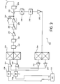
- FIG. 3 a block diagram of another cartesian loop circuit with various power control components is illustrated.
- I and Q signals which are to be transmitted, are provided to the cartesian loop circuit 220 from a digital signal processor (DSP) 222.
- the cartesian loop circuit 220 includes the standard loop components, including the differential amplifiers/loop filters 224 and 226, the upconverter 228, the RF power amplifier chain 229, the coupler 230, the antenna 232 and the downconverter 234.
- the loop circuit 220 also has a plurality of power control components.
- the power control components are pre-loop attenuators 236 and 238, forward path attenuators 240 and 242, forward path amplifier 243, power amplifier by-pass switch 244, feedback path attenuators 246 and 248, feedback path amplifier 250 and I and Q feedback amplifiers 252 and 254.
- the power control components of FIG. 3 provide coarse and fine power control of the output of the signal from the antenna 232.
- the DSP 222 determines the desired output power and provides the control signals to the loop circuit to control the various power control components in accordance with the desired output power.
- the DSP 222 also provides fine power control by controlling the amplitude of the I and Q signals supplied to the loop circuit.
- the DSP 222 in step 260 determines the needed power output level at the antenna 232. Then, in step 262, the DSP 222 or other controlling device sends out control signals that set the coarse power settings of various components in the cartesian loop circuit 220. For example, if attenuators 236, 238, 240 and 242 provide a selectable coarse attenuation level, as the attenuators 104, 106, 132 and 134 in FIG. 2 did, then the DSP 222 selects the desired attenuation level of each of these components, preferably in accordance with preselected values in a look-up table, and then issues control signals to implement the desired attenuation levels.
- the DSP 222 in step 262 calculates the necessary fine power control to implement the desired power output level at the antenna 232.
- the DSP 222 selects the appropriate amplitude of the I and Q signals to finely control the output power level and sends the amplitude controlled I and Q signals to the loop circuit 220.
- the power amplifier by-pass switch 244 implements another power control feature in accordance with another aspect of the present invention.
- the power amplifier 229 is illustrated as having two stages 256 and 258, although more stages can be implemented if desired or needed.
- the by-pass switch 244 is used to by-pass one or more amplification stages as needed to control the output power at the antenna 232. When greater power is needed, the switch 244 is opened and when lower power is needed, the switch 244 is closed. When the switch 244 is closed to bypass an amplifier stage, it is preferred to disable the power amplifier stage 258.
- the control of the switch 244 is preferably accomplished by the DSP 222 although any controlling device in the communication system that knows the desired output power level can control the switch 244.
- FIG. 3 illustrates the switch 244 by-passing a single amplification stage
- the switch 244 can be used to by-pass as many stages as desired.
- the gain control in the forward path shoudl be balanced with a gain control in the feedback path, so as to maintain loop gain.
- the bypass switch 244 it is preferred to control the phase of the loop to account for the change in the phase of the loop caused by a component being switched in and out. The preferred method of controlling the phase of the loop will be described later.
- the attenuators 236 and 238 correspond to the attenuators 104 and 106 of FIG. 2 and can be on/off attenuators as in FIG. 2 which provide a very coarse level of power control.
- the attenuators 236 and 238 can be continuously controlled attenuators that provide a continuous range of attenuation.
- the attenuators 236 and 238 can be used to provide some measure of fine power control.
- the attenuators 240 and 242 and the amplifier 243 of FIG. 3 correspond with the components 132, 134 and 136 in FIG. 2.
- the attenuators 240 and 242 can be 2-4-8-8-16 attenuators or on/off attenuators as in FIG. 2 or they can be continuously variable attenuators.
- the amplifier 243 can provide either on/off gain or continuously variable gain. It should be noted that if the DSP 222 is used to provide power control as previously described, it may be possible to eliminate many of the power control components in the loop 220, particularly those components that provide fine power control.
- the attenuators 246 and 248 and the amplifier 250 of FIG. 3 correspond with the components 148, 150 and 152 in FIG. 2.
- the attenuators 246 and 248 can be 2-4-8-8-16 attenuators or on/off attenuators or, alternatively they can be continuously variable attenuators.
- the amplifier 250 can provide either on/off gain or continuously variable gain.
- any of the power control components in FIG. 3, whether in loop or outside the loop, can be on/off components or can be continuously variable components.
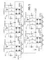
- the circuit diagram of the PIN diode attenuator 150 of FIG. 2 is illustrated.
- the circuit is a five stage 300 to 304 attenuation circuit, the stages providing 2 dB, 4 dB, 8 dB, 8 dB and 16 dB of attenuation, respectively, when enabled.
- Each stage consists of five capacitors C1 to C5, three inductors L1 to L3, four PIN diodes D1 to D4 and three resistors R1 to R3.
- the PIN diodes D1 to D4 are preferably HP/Avantek pin diodes, part number HSMP3895.
- Stage 1 (300) Stage 2 (301) Stage 3 (302) Stage 4 (303) Stage 5 (304) C1 33pF 33pF 33pF 33pF 33pF C2 33pF 33pF 33pF 33pF 33pF C3 3.3pF 3.3pF 3.3pF 3.3pF 3.3pF C4 33pF 33pF 33pF 33pF 33pF 33pF C5 33pF 33pF 33pF 33pF 33pF 33pF L1 39nH 39nH 39nH 39nH 39nH L2 39nH 39nH 39nH 39nH 39nH 39nH L3 39nH 39nH 39nH 39nH 39nH 39nH 39nH 39nH 39nH 39nH 39nH R1 430 ⁇ 220 ⁇ 120 ⁇ 120 ⁇ 68 ⁇ R2 12 ⁇ 27 ⁇ 56 ⁇ 56 ⁇ 150 ⁇ R3 430 ⁇ 220 ⁇ 120 ⁇ 120 ⁇ 120 ⁇ 68 ⁇
- Each stage 300 to 304 has two control signals, CONTROL A and CONTROL B.
- CONTROL A goes low and CONTROL B goes high.
- CONTROL B goes low.
- the circuit of FIG. 5 is preferred in the feedback path 128 because it provides linear high power operation which integrated circuit attenuators can not. Further, the attenuator circuit of FIG. 5 is preferred over relays as it eliminates large mechanical devices and operates more quickly.
- the cartesian loop circuit of the present invention includes a noise filter 138 in the loop, specifically in the forward path 126 of the loop.
- the filter 138 is preferably a bandpass filter having a bandwidth equal to or greater than the complete bandwidth over which the system transmits. So, for example, in a frequency hopping system where a plurality of frequencies are used, the bandwidth of the filter must permit transmission of all frequencies and protect the received frequencies from extraneous noise created by the loop.
- the noise filter 138 blocks frequencies generated by loop comonents that are within the receive band of a communication system. Any filter that accomplishes these functions can be used.
- the purpose of the noise filter 138 is to filter out the noise created by the components in the loop.
- the baseband components in the loop have wideband characteristics which tend to create noise over a wide range of frequencies. Further, there is typically a great deal of gain in the loop so that the loop noise, including the wideband noise, is amplified.
- the noise filter 138 filters out this noise.
- the noise filter 138 is located In the forward path 126 after the upconverter 130 and after the power control components 132, 134 and 136 but before the power amplifier 140.
- the location of the filter 138 before the power amplifier 140 allows the filter 138 to operate on lower power signals, thereby making the filter 138 less expensive.
- the filter 138 can be located in other positions as well.
- the filter 138 can be located in the forward path 126 after the upconverter 130.
- the filter 138 will not filter out the noise created by the power control components 132, 134 and 136.
- the filter 138 can also be located after the power amplifier 140, however, this location requires the filter 138 to be designed to handle a much higher power signal.
- the filter 138 is particularly useful in permitting full duplex operation of the communication device employing the cartesian loop transmitter of FIG. 2.
- duplex operation the transmissions are at a high power level and at the same time the signals are received at much lower power levels. Accordingly, the duplexer 146 provides separation of the high power transmit signal and the low power receive signal.
- the duplexer 146 does not fully suppress the noise in the receive band.
- the noise filter 138 provides improved receive band noise suppression, thereby improving full duplex operation in a radio communication system.
- the bandpass filter 138 It is preferred, but not necessary to, implement the bandpass filter 138 with a surface acoustic wave (SAW) device.
- SAW surface acoustic wave
- the SAW filter 138 provides improved phase response and improved linearity than other types of bandpass filters.
- a preferred SAW filter 138 is part number FAR.F5CC.902M50-L2EZ made by Fujitsu. Note that the center frequency of this SAW filter 138 is 902MHz while the upconverter 130 converts the baseband I and Q signals to 896 to 901 MHz. Since the bandwidth of the noise filter 138 is wide enough, the SAW filter 138 operates acceptably.
- the cartesian loop transmitter of the present invention includes DC offset nulling circuitry 300 and 302.
- the first DC offset nulling circuit 300 includes a differential amplifier 302 and a sample and hold 306.
- the second DC offset nulling circuit 302 also includes a differential amplifier 308 and a sample and hold 310.
- circuits 300 and 302 operate the same way and perform the same functions, except the circuit 300 nulls DC offsets in the I path and the circuit 302 nulls DC offsets in the Q path. Therefore, while the following describes the operation of the first circuit 300, it is equally applicable to both circuits 300 and 302.
- the differential amplifier 304 from the first DC offset nulling circuit 300 has a first input from the output of the loop filter 118 and a second input from the reference output of the upconverter 130. This reference outputs the mid-rail reference of the power supply. In the circuit of FIG. 2, a single rail supply of about 12 volts is used so that the reference output is about 6 volts. If a dual power supply were used, for example + 6 volts and - 6 volts, then the mid-rail output would be about 0 volts. Thus, the differential amplifier 304 determines the DC offset between the loop filter 118 and the mid-rail reference output of the upconverter 130. Alternative measures of DC offset can also be utilized.
- Line A in FIG. 6 represents the timing associated with a particular time slot in a TDMA type communication system wherein communications are provided in a plurality of time slots.
- Line B represents the control signal which is provided to the power amplifier module 140 to enable and disable the forward path 126.
- TxON is high, the power amplifier 140 is enabled and the forward path 126 provides an amplified signal.
- the power amplifier 140 When TxON is low, the power amplifier 140 is disabled and the forward path 126 is disabled so that no signal is provided to the antenna 148 or to the feedback path 128.
- the synthesizers needed to generate the frequencies for the communication system and for the upconverter 130 and the downconverter 156 for the cartesian loop transmitter are enabled as indicated in line C of FIG. 6.
- the synthesizers become available with acceptable accuracy as indicated in line D.
- Line E represents the preferred control signal for the sample and hold 306.
- the sample and hold 306 begins to sample the output of the differential amplifier 304.
- the sample and hold 306 completes a feedback loop around the amplifier 118.
- the action of the feedback loop causes the voltage on the charging capacitor of the sample and hold 306 to acquire a value sufficient to minimize any DC error between the output of the amplifier 118 and the mid rail reference.
- the sample and hold 306 is switched into hold mode as line E goes low.
- TxOn Line B is preferably disabled during the sampling process so that the forward path 126 is disabled and the DC offset being measured results from the DC offsets of the components in the reverse path 128.
- the negative value of the DC offset appears on the output of the sample and hold 306.
- the output of the sample and hold 306 is connected to the summing point 108.
- the complementary value of the DC offset measured during the disablement of the forward path is added to the Input to the loop filter 118, canceling the DC offset created by the components in the feedback path 128.
- the control signal TxON goes high, thereby enabling operation of the forward path 126 before the time slot becomes active.
- the negative of the measured DC offset is added to the signal during the active time slot to null the DC offset.
- the local oscillator affects the DC offsets
- the loop circuit of FIG. 2 includes an instability detection circuit 400.
- the loop is designed with an appropriate amount of gain and phase delay so as to maintain the stability of the loop. Nevertheless, the loop can become unstable for number of reasons. For example, loop instability can be caused by too much loop gain or poor antenna VSWR. When the loop goes unstable, it results in the generation of out of band frequencies that generally cause the transmitted signal to break the transmission mask of the communication device.
- the instability detection circuit 400 detects when the loop becomes unstable and then causes appropriate action to be taken to avoid breaking the transmission mask.
- the instability detection circuit 400 preferably includes a filter 402, an envelope detector 404 and a comparator 406.
- the circuit 400 is preferably connected to the loop circuit within the feedback path 126, after the downconverter. This location allows detection of signals at the baseband frequency regardless of the frequency at which the signal is transmitted.
- the circuit 400 can be connected to other points in the loop, but it is preferred to connect the instability detection circuit 400 to the loop to detect a baseband frequency as it simplifies the design of the filter 402.
- the signal at the output of the feedback path 128 should mainly include frequencies within the bandwidth of the I and Q signals.
- a signal 408 -- having bandwidth, bw -- is illustrated in FIG. 7.
- the filter 402 is preferably a high pass filter with a cutoff frequency, f HP .
- the envelope detector 404 therefore, detects no signal.
- the comparator 406 which is comparing the output of the envelope detector 404 to a threshold th determines that there is no unwanted signals present in the loop, which indicates that the loop is operating in a stable condition.
- the signal at the output of the feedback path 128 will include frequencies outside the bandwidth of the feedback signal 408.
- a typical signal 410 that results from unstable loop conditions is illustrated in FIG. 8.
- the signal 410 includes the feedback signal but also includes the noise signal 414.
- the filter 402 in the instability detection circuit 400 blocks the feedback signal, but passes the noise signal 414.
- the envelope detector 404 detects the presence of the noise signal 414 and passes the envelope of the signal 414 to the comparator 406. If the noise signal 414 has an amplitude that exceeds the threshold, th, the comparator outputs an active signal to indicate that the loop is operating in an unstable condition.
- the output of the instability circuit 400 is output to a DSP such as the DSP 222 shown in FIG. 3.
- the DSP preferably performs one of several functions. First, the DSP attempts to adjust the phase of the loop. The method by which the phase is adjusted will be discussed later. If that action does not bring the loop back into stable operation, the DSP attempts to control the power in either the forward path 126 or the feedback path 128. While it is normally preferred to adjust the power control in a balanced fashion, as previously discussed, in this case the power adjustment is made differentially so that the power is adjusted in only one part of the loop. If this does not return the loop to stable operation, then the DSP attempts to reduce the power output of the circuit in discrete steps. If this still does not return the loop to stable operation, the DSP shuts down the transmitter.
- the loop circuit of FIG. 2 includes a temperature sensor 416 which detects the operating temperature of the cartesian loop transmitter.
- the output of the temperature sensor 416 is connected to two comparators 418 and 420.
- the first comparator 418 compares the output of the temperature sensor 416 to a first threshold, th1, and the second comparator compares the output of the temperature sensor to a second threshold, th2.
- the output of the cartesian loop can break the transmission mask.
- the comparator 418 outputs an active signal on OVERHEAT 1.
- the signal OVERHEAT1 is sent to the system controller, such as the DSP 222 in FIG. 3 or any other system controller.
- the system controller preferably causes a lower power to be transmitted by controlling the attenuation or gain of the power control components in the cartesian loop to cause a lower power output signal to be provided at the antenna 148.
- the system controller can adjust the attenuators 104, 106, 132, 134, or 150 or the amplifiers 154, or any other device to lower the power output.
- the lower power output causes the signal to be transmitted within the defined transmission mask.
- the system controller preferably shuts down the cartesian loop transmitter. This ensures that the transmission mask will not be broken.
- the loop gain can be altered differentially -- that is, in either the forward path or the feedback path without balancing -- to try to restore proper operation within a transmission path.
- the phase of the loop can be changed. Any of these actions can be taken in any order with any priority.
- the loop circuit of FIG. 2 also includes two comparators 422 and 424, which are connected to the power supply of the cartesian loop transmitter.
- the first comparator 422 compares the output of the power supply, V, to a first threshold, th1, and the second comparator 424 compares the output of the power supply to a second threshold, th2.
- the output of the cartesian loop can break the transmission mask if the loop is left to operate without any change.
- the comparator 422 when the power supply falls below the threshold, th1, the comparator 422 outputs an active signal on UNDERVOLTS1.
- the signal UNDERVOLTS1 is sent to the system controller, such as the DSP 222 in FIG. 3 or any other system controller.
- the system controller preferably causes a lower power to be transmitted by controlling the attenuation or gain of the power control components in the cartesian loop to cause a lower power output signal to be provided at the antenna 148.
- the system controller can adjust the attenuators 104, 106, 132, 134, or 150 or the amplifiers 154, or any other device to lower the power output.
- the lower power output causes tne signal to be transmitted within the defined transmission mask.
- the system controller preferably shuts down the cartesian loop transmitter. This ensures that the transmission mask will not be broken.
- the loop gain can be altered differentially -- that is, in either the forward path or the feedback path without balancing -- to try to restore proper operation within a transmission path.
- the phase of the loop can be changed. Any of these actions can be taken in any order with any priority.
- the shaping circuit 450 for the case of FIG. 2, is a simple RC filter, using a resistance of 2.2 k ⁇ and a capacitance of 22 nF. The shaping circuit 450 therefore causes the input to the power pin of the power amplifier 140 to increase slowly when it is first turned on during an active slot.
- This delay allows the loop gain around the loop 126 and 128 to be established before a high power signal is transmitted, thereby allowing the loop to implement its corrections and to prevent spurious signals that may be caused by the components in the loop before stable operation begins. For example, DC offsets in the forward path are not corrected until the signal has traveled around the loop. Also there are local oscillator leakage problems to contend with. By delaying the transmission of the signal for a length of time sufficient for the signal to travel around the loop, improved operation is achieved.
- the phase of the loop can be set by a manual phase adjuster 460 and by a computer controlled phase adjuster 462.
- the manual phase adjuster 460 can be used to set up the phase of the loop.
- the computer controlled phase adjuster 462, in accordance with another aspect of the present invention, is controlled in accordance with the power output levels of the loop and with the frequency of the signal being transmitted, to cause a shift in the local oscillator that drives the downconverter 156.
- the control computer determines the transmit frequency of the signal.
- the control computer accesses a lookup table to determine the appropriate phase control setting for the downconverter's 156 local oscillator and then sets the computer controlled phase adjuster 462 accordingly.
- the lookup table divides the band into three bands and controls the phase adjuster 462 in approximately 20° steps.
- the exact implementation will vary with each application.
- the phase of the loop is also preferably controlled as a function of the power control of the loop. As the power control components in the loop are switched In and out, the phase of the loop changes. Therefore, in accordance with the present invention the control computer, such as a DSP 222, maintains a table of the possible loop phases that can result when the various loop power control components are switched in and out of the loop. As part of the power control function, the DSP 222 accesses the table to determine the appropriate loop phase for the particular loop configuration and controls the phase adjuster 462 to adjust the loop phase accordingly. Thus, as each power control component is switched in and out, the loop phase is adjusted.
- the control computer such as a DSP 222
- the control computer changes the phase of the loop as any of the attenuators 132, 134, 150 and 152 or the amplifiers 136 and 154 are switched in or out.
- the control computer changes the phase of the loop as any of the power control components 224, 226, 240, 242, 243, 256, 258, 246, 248, 250, 252 or 254 are switched in or out of the loop. This includes when the bypass switch 244 switches the amplifier stage 258 in or out of the loop.
Landscapes
- Engineering & Computer Science (AREA)
- Power Engineering (AREA)
- Physics & Mathematics (AREA)
- Nonlinear Science (AREA)
- Transmitters (AREA)
- Amplifiers (AREA)
- Arrangements For Transmission Of Measured Signals (AREA)
- Measuring Fluid Pressure (AREA)
- Control Of Amplification And Gain Control (AREA)
- Cash Registers Or Receiving Machines (AREA)
- Steroid Compounds (AREA)
- Liquid Crystal Substances (AREA)
Abstract
Description
- This invention generally relates to radio transmitters. More specifically, it relates to apparatus and method for providing linear radio transmitters via cartesian loop circuitry.
- Today's radio communications systems typically operate in narrowly defined bands of frequency. Consequently, the transmitters in radio communication systems require power amplifiers that are capable of operating in a highly linear fashion to maintain the spectral efficiency, thereby minimizing the resulting interference.
- The use of cartesian loop circuits to achieve linear power amplification in communication system transmitters is known in the art. A known cartesian loop circuit is shown in FIG. 1 and is described in an article entitled "RF Linear Amplifier Design," by P.B. Kenington and A. Batsman, published in the Proceedings of RF Expo West at pages 223 to 232 in March of 1994.
- The cartesian loop circuit of FIG. 1, however, has several limitations. One general limitation is the inability to provide adequate power control, a necessary function in most communication system transmitters. By way of example only, existing circuits do no provide an adequate range of power control. Further, existing circuits also do not provide adequate fine power control. There are other limitations in the power control offered by existing cartesian loop circuits.
- Existing cartesian loop circuits also do not provide any noise filtering to remove the noise introduced by the cartesian loop. Thus, existing cartesian loop circuits provide noisy operation. Existing cartesian loop circuits also do not provide adequate calibration techniques to compensate for DC offset of components and to compensate for phase variations in the cartesian loop. All of these limitations place a limit on the accuracy of operation.
- Other limitations include the lack of instability detection, the lack of adaptive operation during overheat situations and during undervoltage situations and the lack of any type of detection of the transmission mask to ensure the proper operation of the cartesian loop transmitter.
- In view of these and other limitations, new and improved cartesian loop circuitry is needed, particularly for use in linear transmitters in radio communication systems.
- W095/06354 discloses a radio transmitter with a cartesian feedback circuit. In a training mode of operation, a training signal is applied to the power amplifier, and the linearizing feedback circuit is adjusted.
- The present invention provides method and apparatus for nulling DC offsets in a feedback path of a cartesian loop that consists of a forward path and the feedback path, thereby minimizing degradation of the performance of the cartesian loop. In accordance with the method of nulling offsets, the operation of the forward path is disabled and the DC offset in the feedback path is sensed and stored. The DC offset in the feedback path is then subtracted out while the forward path is enabled. The downconverter is preferably driven with its local oscillator during this process since the local oscillator can affect the DC offset. In accordance with a preferred embodiment, if sytem timing constraints do not permit the local oscillator to look at its specified stability, the storing of the DC offset is done when the local oscillators have reached a predetermined stability.
- The DC offset nulling is preferably performed with a sample and hold that senses and acquires the DC offset in the feedback path when the forward path is disabled. The forward path is disabled preferably by disabling a power amplifier in the forward path.
- Specifically, according to one aspect of the invention, there is provided a method of transmitting baseband signals with a cartesian loop circuit, the cartesian loop circuit having a forward path, a feedback path, an upconverter and a downconverter and frequency synthesizers which supply the cartesian loop with local oscillators for the upconverter and the downconverter, the method comprising the steps of:
- disabling the operation of the forward path;
- sensing and storing the DC offset in the feedback path while the forward path is disabled, before the time slot in which communication is to take place becomes active, when the frequency synthesizers have reached a predetermined stability; and
- subtracting the DC offset in the feedback path.
-
- According to a second aspect of the invention, there is provided a cartesian loop for transmitting baseband signals, comprising:
- a forward path having a first input for the baseband signals and a second input, the forward path including means to upconvert the input signals to an RF signal for transmission;
- a feedback path for providing an error signal input indicative of the non-linearity of the forward path to the second input of the forward path, the feedback path having an input from the forward path and means to downconvert the input from the forward path;
- control means for disabling the input to the feedback path;
- frequency synthesizers for supplying local oscillators for the means to upconvert the input signals and for the means to downconvert the input from the forward path;
- means for sensing and acquiring the DC offset in the feedback path when the forward path is disabled, and before the time slot in which communication is take place becomes active, and when the frequency synthesizers have reached a predetermined stability; and
- means for subtracting the DC offset from the feedback path. accomplished by ramping the power control signal to an output power amplifier in the forward path of the cartesian loop circuit.
-
- In accordance with another aspect of the present invention, apparatus and method for simply controlling the power output of the cartesian loop transmitter are provided. In accordance with the method, one or more stages of a multi-stage power amplifier in the forward path of a cartesian loop are bypassed with a bypass switch when lower power output is desired. It is preferred to control the phase of the cartesian loop as stages are bypassed to account for the changes in loop phase.
- In accordance with another aspect of the present invention, apparatus and method for controlling the power output of a cartesian loop by selectable loop attenuation with a PIN diode circuit are provided. In accordance with the apparatus, the forward path of the loop includes a first input for receiving baseband signals, a second input, means to upconvert the input signals to a signal to be transmitted, an attenuator having selectable attenuation and a plurality of power amplifier stages. The feedback path includes an input from the forward path, a PIN diode attenuator having selectable attenuation and means to downconvert and an output that provides a feedback signal to the second input. It is preferred to control the attenuation so that the attenuation removed in the forward path equals the attenuation added in the reverse path and vica versa.
- In accordance with a further aspect of the present invention, apparatus
-
- FIG. 1 illustrates a block diagram of a known cartesian loop circuit;
- FIG. 2 illustrates a block diagram of a cartesian loop circuit which implements several aspects of the present invention;
- FIG. 3 illustrates a block diagram of a cartesian loop with power control features in accordance with a preferred embodiment of the present invention;
- FIG. 4 illustrates the process by which a digital signal processor controls the power output of a cartesian loop circuit in accordance with one aspect of the present invention;
- FIG. 5 illustrates a PIN diode circuit in accordance with a preferred embodiment of the present invention;
- FIG. 6 illustrates a timing diagram showing the operation of the DC nulling circuit of FIG. 2 in accordance with one aspect of the present invention; and
- FIG. 7 illustrates a typical baseband signal generated by the loop during stable operation and a typical baseband signal generated by the loop during unstable operation.
-
- The invention will now be described in connection with certain illustrated embodiments; however, it should be clear to those skilled in the art that various modifications, additions and subtractions can be made without departing from the spirit and scope of the claims.
- Referring to FIG. 1, a known cartesian loop circuit is illustrated. The circuit receives I and Q inputs at baseband frequency in the
differential amplifiers unconverter 14. The upconverted signals are amplified by an amplifier stage, represented by a pair ofamplifiers antenna 20. - The
transmission path 22 is referred to as the forward path. Theforward path 22 is similar to the circuitry found in any transmitter. In the circuit of FIG. 1, however, theamplifiers feedback path 24 provided by cartesian loop circuits. - The input to the
feedback path 24 is generated by acoupler 26 which outputs a portion of the signal from theforward path 22 to thefeedback path 24. The coupled signal is downconverted to the baseband frequency by adownconverter 28. The downconverted signals are input to thedifferential amplifiers amplifiers - Referring to FIG. 2, a preferred embodiment of a cartesian loop circuit that implements several aspects of the present invention is illustrated. Differential I and Q inputs are supplied to
differential amplifiers amplifiers attenuators attenuators points - The summing
point 108 provides the input to aloop filter 112 and the summingpoint 110 provides the input to aloop filter 114. The loop filters 112 and 114 are implemented as integrators withamplifiers capacitors - The loop filters 112 and 114 provide the outputs to the
forward path 126. As previously described, one input to the summingpoints points feedback path 128 which provides a measure of the error of the operation of the cartesian loop. - The outputs from the loop filters 112 and 114 are input to an
upconverter 130. Theupconverter 130 converts the I and Q outputs from the loop filters 112 and 114, which are at a baseband frequency, to a RF frequency. In this case, the preferred RF frequency is 900MHz. - The RF signal from the
upconverter 130 is sent to anattenuator 132 and then to anotherattenuator 134. The signal is then sent to anamplifier 136 and then to abandpass filter 138. The signal is then sent to apower amplifier module 140 which amplifies the signal prior to transmission. The amplified signal is then sent from thepower amplifier 140 through acoupler 142, anisolator 144 and aduplexer 146 to anantenna 148 which transmits the signals. - The
coupler 142 transmits a portion of the signal from theforward path 126 to thefeedback path 128. In thefeedback path 128, the signal is sent to anattenuator 148, then to anattenuator 150 and then to an amplifier stage consisting of aswitchable attenuator 152 and aswitchable amplifier 154. The power controlled signal is then sent to adownconverter 156. Thedownconverter 156 converts the signal in thefeedback path 128 to a baseband signal. - The I and Q outputs from the
downconverter 156 are sent through theamplifiers amplifiers amplifier 160 provides the output to the summingpoint 108 and theamplifier 164 provides the output to the summingpoint 110. - The power control features provided in the embodiment of the cartesian loop shown in FIG. 2 in accordance with several aspects of the present invention will now be discussed. The I and Q inputs are initially input through the
attenuators attenuators attenuators register 166 and thedriver 168 from the communication system. Thus, theattenuators - Then the I and Q signals are input to the cartesian loop circuit and upconverted by the
upconverter 130 to a frequency between 896MHz to 901 MHz, or some other desired frequency. After the upconversion, the signal in theforward path 126 is again power controlled by theattenuator 132. thePIN diode attenuator 134 and theamplifier 136. Theattenuator 132 in the case of FIG. 2 is a 2-4-8-8-16 attenuation integrated circuit that allows the following attenuations to be switched in and out of the forward path 126: 2dB, 4dB, 8dB, 8dB and 16dB. Theattenuator 132, therefore, provides up to 32 dB of attenuation in 2 dB steps. As such, theattenuator 132 can be used to provide fine power control in 2dB increments in theforward path 126. Theattenuator 132 can be implemented by the part number RF2410, made by RF MicroDevices. Theattenuator 132 is digitally controlled by the control signals CONTROL which are provided by the communication system. - The
PIN diode attenuator 134 preferably provides 15 dB of attenuation when theattenuator 134 is enabled and 0dB of attenuation when not enabled. Theattenuator 134 is preferably enabled and disabled under control of the control signal CONTROL from the communication system. Thus, theattenuator 134 provides gross power control in theforward path 126. - The
amplifier 136 in theforward path 126 provides 30dB of gain. Then, after filtering by thenoise bandpass filter 138, thepower amplifier 140 provides another 30 to 40 dB of gain. In accordance with one embodiment of the present invention, the power output of the cartesian loop can also be controlled by varying the signal on the power pin of thepower amplifier 140. So, for example, if a Hitachi PF0121 power amplifier is used in FIG.2, the power output of theamplifier 140 can be decreased by decreasing the signal POWER CONTROL which results in decreased output from the loop. Conversely, the power output of theamplifier 140 can be increased by increasing the signal POWER CONTROL which results in increased output from the loop. As gain is increased or decreased in theamplifier 140, a corresponding change should be implemented in thefeedback path 128, so that overall loop gain is maintained. After power amplification, the signal is then output through theantenna 148. - So far, the circuit of FIG. 2 provides 15 dB of attenuation before the loop. Then, the
forward path 126 of the loop provides up to 47 dB of attenuation. All of the attenuation is under control of the system controller in the communication system. Theforward path 126 also provides a first 30 dB amplification stage and a second 30 to 40 dB amplification stage before the signal is provided to theantenna 148. It is understood that the amplifiers shown in FIG. 2 in fact represent several stages of amplifiers. - The power control in the
feedback path 128 will now be discussed. As stated before, thefeedback path 128 starts with thecoupler 142 which, in the case of FIG. 2, couples approximately 1.0% of the signal from theforward path 126. The coupled signal is then attenuated by thelevel set attenuator 148. The level set attenuator is provided to allow calibration of the loop to compensate for tolerance variations from circuit to circuit and to set the initial power output of the loop circuit. - Then the signal is attenuated by a 2-4-8-8-16
attenuator 150. Theattenuator 150 balances theattenuator 132 in theforward path 126. Theattenuator 150 is preferably a PIN diode circuit which provides a total of up to 32 dB of attenuation in 2 dB increments. The selection of the amount of attenuation is provided by control signals from the system controller of the communication system which are stored in theregister 166. - The signal is then passed to a switchable amplification stage that includes the 0
dB attenuator 152 and the 15dB amplifier 154. When amplification of the output signal is desired by the system controller of the communication system, theamplifier 154 is disabled and the 0 dB attenuator is enabled by the control signals from theregister 166. When a lower power output is desired, the system controller enables theamplifier 154 and disables theattenuator 152 so that the signal in the feedback path is amplified. - When attenuation or gain is switched in and out of either the
forward path 126 or thefeedback path 128, it is preferred to switch in or out an equal amount of attenuation or gain in the other path. Doing this maintains the balance of the loop by preventing a change in overall loop gain despite variations in output power. For example, to keep the loop balanced, it is preferred to balance a gain in power in theforward path 126 with an attenuation of power in thefeedback path 128. Similarly, it is preferred to balance an attenuation of power in theforward path 126 with a gain of power in thefeedback path 128. Thus, if attenuation is switched in theforward path 126, it is preferred to switch out an equal attenuation in thefeedback path 128. - The circuit of FIG. 2 provides fine and coarse control of power output with components inside and outside the loop. In the case of FIG. 2, fine control refers to steps of 1 to 2 dB of power control while coarse control refers to larger steps of power control, although in other systems the steps of fine and coarse control may have different values. In FIG. 2, 15 dB of power control is provided outside the loop by the
attenuators attenuators attenuators amplifier 154, the use of each of these components being balanced as previously explained. - FIG. 2 illustrates a particular embodiment of a cartesian loop in accordance with the present invention. In FIG. 3, a block diagram of another cartesian loop circuit with various power control components is illustrated. In FIG. 3, I and Q signals, which are to be transmitted, are provided to the
cartesian loop circuit 220 from a digital signal processor (DSP) 222. Thecartesian loop circuit 220 includes the standard loop components, including the differential amplifiers/loop filters upconverter 228, the RFpower amplifier chain 229, thecoupler 230, theantenna 232 and thedownconverter 234. - The
loop circuit 220 also has a plurality of power control components. The power control components arepre-loop attenuators forward path attenuators forward path amplifier 243, power amplifier by-pass switch 244,feedback path attenuators feedback path amplifier 250 and I andQ feedback amplifiers - The power control components of FIG. 3 provide coarse and fine power control of the output of the signal from the
antenna 232. TheDSP 222, in accordance with one aspect of the present invention, determines the desired output power and provides the control signals to the loop circuit to control the various power control components in accordance with the desired output power. TheDSP 222 also provides fine power control by controlling the amplitude of the I and Q signals supplied to the loop circuit. - Referring to FIG. 4, In accordance with one aspect of the present invention, the
DSP 222, or other controlling device, instep 260 determines the needed power output level at theantenna 232. Then, instep 262, theDSP 222 or other controlling device sends out control signals that set the coarse power settings of various components in thecartesian loop circuit 220. For example, ifattenuators attenuators DSP 222 selects the desired attenuation level of each of these components, preferably in accordance with preselected values in a look-up table, and then issues control signals to implement the desired attenuation levels. Simultaneously, theDSP 222, instep 262 calculates the necessary fine power control to implement the desired power output level at theantenna 232. TheDSP 222 then selects the appropriate amplitude of the I and Q signals to finely control the output power level and sends the amplitude controlled I and Q signals to theloop circuit 220. - Referring back to FIG. 3, the power amplifier by-
pass switch 244 implements another power control feature in accordance with another aspect of the present invention. Thepower amplifier 229 is illustrated as having twostages pass switch 244 is used to by-pass one or more amplification stages as needed to control the output power at theantenna 232. When greater power is needed, theswitch 244 is opened and when lower power is needed, theswitch 244 is closed. When theswitch 244 is closed to bypass an amplifier stage, it is preferred to disable thepower amplifier stage 258. The control of theswitch 244 is preferably accomplished by theDSP 222 although any controlling device in the communication system that knows the desired output power level can control theswitch 244. While FIG. 3 illustrates theswitch 244 by-passing a single amplification stage, theswitch 244 can be used to by-pass as many stages as desired. Of course the gain control in the forward path shoudl be balanced with a gain control in the feedback path, so as to maintain loop gain. When thebypass switch 244 is utilized, it is preferred to control the phase of the loop to account for the change in the phase of the loop caused by a component being switched in and out. The preferred method of controlling the phase of the loop will be described later. - In FIG. 3, the
attenuators attenuators attenuators attenuators - The
attenuators amplifier 243 of FIG. 3 correspond with thecomponents attenuators amplifier 243 can provide either on/off gain or continuously variable gain. It should be noted that if theDSP 222 is used to provide power control as previously described, it may be possible to eliminate many of the power control components in theloop 220, particularly those components that provide fine power control. - The
attenuators amplifier 250 of FIG. 3 correspond with thecomponents attenuators amplifier 250 can provide either on/off gain or continuously variable gain. - It is also possible to provide power control of the output signal with the
amplifiers downconverter 234 in the feedback path. Another possible method of power control is to place anattenuator 259 in the output path. Further, any of the power control components in FIG. 3, whether in loop or outside the loop, can be on/off components or can be continuously variable components. - Referring to FIG. 5, the circuit diagram of the
PIN diode attenuator 150 of FIG. 2 is illustrated. The circuit is a fivestage 300 to 304 attenuation circuit, the stages providing 2 dB, 4 dB, 8 dB, 8 dB and 16 dB of attenuation, respectively, when enabled. Each stage consists of five capacitors C1 to C5, three inductors L1 to L3, four PIN diodes D1 to D4 and three resistors R1 to R3. The PIN diodes D1 to D4 are preferably HP/Avantek pin diodes, part number HSMP3895. The values of these components in each stage, in accordance with a preferred embodiment of the present invention, are as given in the table below:Stage 1
(300)Stage 2
(301)Stage 3
(302)Stage 4
(303)Stage 5
(304)C1 33pF 33pF 33pF 33pF 33pF C2 33pF 33pF 33pF 33pF 33pF C3 3.3pF 3.3pF 3.3pF 3.3pF 3.3pF C4 33pF 33pF 33pF 33pF 33pF C5 33pF 33pF 33pF 33pF 33pF L1 39nH 39nH 39nH 39nH 39nH L2 39nH 39nH 39nH 39nH 39nH L3 39nH 39nH 39nH 39nH 39nH R1 430Ω 220Ω 120Ω 120Ω 68Ω R2 12Ω 27Ω 56Ω 56Ω 150Ω R3 430Ω 220Ω 120Ω 120Ω 68Ω - Each
stage 300 to 304 has two control signals, CONTROL A and CONTROL B. To activate a stage, ie. to utilize the stage to attenuate, CONTROL A goes low and CONTROL B goes high. To deactivate a stage, CONTROL A goes high and CONTROL B goes low. - The circuit of FIG. 5 is preferred in the
feedback path 128 because it provides linear high power operation which integrated circuit attenuators can not. Further, the attenuator circuit of FIG. 5 is preferred over relays as it eliminates large mechanical devices and operates more quickly. - Referring to FIG. 2, the cartesian loop circuit of the present invention includes a
noise filter 138 in the loop, specifically in theforward path 126 of the loop. Thefilter 138 is preferably a bandpass filter having a bandwidth equal to or greater than the complete bandwidth over which the system transmits. So, for example, in a frequency hopping system where a plurality of frequencies are used, the bandwidth of the filter must permit transmission of all frequencies and protect the received frequencies from extraneous noise created by the loop. Thus, thenoise filter 138 blocks frequencies generated by loop comonents that are within the receive band of a communication system. Any filter that accomplishes these functions can be used. - The purpose of the
noise filter 138 is to filter out the noise created by the components in the loop. The baseband components in the loop have wideband characteristics which tend to create noise over a wide range of frequencies. Further, there is typically a great deal of gain in the loop so that the loop noise, including the wideband noise, is amplified. Thenoise filter 138 filters out this noise. - Note that, in FIG. 2, the
noise filter 138 is located In theforward path 126 after theupconverter 130 and after thepower control components power amplifier 140. This is the preferred location of thebandpass filter 138 as it allows noise created by theupconverter 130 and thepower control components filter 138 before thepower amplifier 140 allows thefilter 138 to operate on lower power signals, thereby making thefilter 138 less expensive. Nevertheless, thefilter 138 can be located in other positions as well. For example, thefilter 138 can be located in theforward path 126 after theupconverter 130. This location of thefilter 138, however, will not filter out the noise created by thepower control components filter 138 can also be located after thepower amplifier 140, however, this location requires thefilter 138 to be designed to handle a much higher power signal. - The
filter 138 is particularly useful in permitting full duplex operation of the communication device employing the cartesian loop transmitter of FIG. 2. In duplex operation, the transmissions are at a high power level and at the same time the signals are received at much lower power levels. Accordingly, theduplexer 146 provides separation of the high power transmit signal and the low power receive signal. However, when the loop circuit creates wideband noise, theduplexer 146 does not fully suppress the noise in the receive band. Thus, thenoise filter 138 provides improved receive band noise suppression, thereby improving full duplex operation in a radio communication system. - It is preferred, but not necessary to, implement the
bandpass filter 138 with a surface acoustic wave (SAW) device. TheSAW filter 138 provides improved phase response and improved linearity than other types of bandpass filters. Apreferred SAW filter 138 is part number FAR.F5CC.902M50-L2EZ made by Fujitsu. Note that the center frequency of thisSAW filter 138 is 902MHz while theupconverter 130 converts the baseband I and Q signals to 896 to 901 MHz. Since the bandwidth of thenoise filter 138 is wide enough, theSAW filter 138 operates acceptably. - Referring to FIG. 2, the cartesian loop transmitter of the present invention includes DC offset
nulling circuitry nulling circuit 300 includes adifferential amplifier 302 and a sample and hold 306. The second DC offsetnulling circuit 302 also includes adifferential amplifier 308 and a sample and hold 310. - Both
circuits circuit 300 nulls DC offsets in the I path and thecircuit 302 nulls DC offsets in the Q path. Therefore, while the following describes the operation of thefirst circuit 300, it is equally applicable to bothcircuits - The
differential amplifier 304 from the first DC offsetnulling circuit 300 has a first input from the output of theloop filter 118 and a second input from the reference output of theupconverter 130. This reference outputs the mid-rail reference of the power supply. In the circuit of FIG. 2, a single rail supply of about 12 volts is used so that the reference output is about 6 volts. If a dual power supply were used, for example + 6 volts and - 6 volts, then the mid-rail output would be about 0 volts. Thus, thedifferential amplifier 304 determines the DC offset between theloop filter 118 and the mid-rail reference output of theupconverter 130. Alternative measures of DC offset can also be utilized. - The measured value of the DC offset from the
differential amplifier 304 is sent to the input of the sample and hold 306. Referring to FIG. 6, a timing diagram of the operation of the sample and hold 306 is illustrated. Line A in FIG. 6 represents the timing associated with a particular time slot in a TDMA type communication system wherein communications are provided in a plurality of time slots. When line A is high, the particular time slot is potentially active (that is, if a subscriber assigned to the time slot is trying to communicate with someone) and when the line A is low, the particular time slot is inactive. Line B represents the control signal which is provided to thepower amplifier module 140 to enable and disable theforward path 126. When TxON is high, thepower amplifier 140 is enabled and theforward path 126 provides an amplified signal. When TxON is low, thepower amplifier 140 is disabled and theforward path 126 is disabled so that no signal is provided to theantenna 148 or to thefeedback path 128. The synthesizers needed to generate the frequencies for the communication system and for theupconverter 130 and thedownconverter 156 for the cartesian loop transmitter are enabled as indicated in line C of FIG. 6. The synthesizers become available with acceptable accuracy as indicated in line D. - Line E represents the preferred control signal for the sample and hold 306. When line E goes high, the sample and hold 306 begins to sample the output of the
differential amplifier 304. The sample and hold 306 completes a feedback loop around theamplifier 118. The action of the feedback loop causes the voltage on the charging capacitor of the sample and hold 306 to acquire a value sufficient to minimize any DC error between the output of theamplifier 118 and the mid rail reference. When a stable charge value is reached, the sample and hold 306 is switched into hold mode as line E goes low. Note that TxOn (Line B) is preferably disabled during the sampling process so that theforward path 126 is disabled and the DC offset being measured results from the DC offsets of the components in thereverse path 128. - Once the control signal on Line E goes low, the negative value of the DC offset appears on the output of the sample and hold 306. The output of the sample and hold 306 is connected to the summing
point 108. Thus, the complementary value of the DC offset measured during the disablement of the forward path is added to the Input to theloop filter 118, canceling the DC offset created by the components in thefeedback path 128. At some later time, the control signal TxON goes high, thereby enabling operation of theforward path 126 before the time slot becomes active. The negative of the measured DC offset is added to the signal during the active time slot to null the DC offset. - Since the local oscillator affects the DC offsets, it is preferred to drive the
downconverter 156 with a local oscillator during acquisition of the DC offset value. It is preferred to allow the synthesizers that supply the local oscillators to theupconverter 130 and thedownconverter 156 to get as close as possible to their specified stability since the local oscillator will affect the DC offset of the upconverter and the downconverter. There can be, however, system timing constraints that require a tradeoff so that the DC offset measurement is taken before the synthesizers reach their specified stability. In this case, the DC offset measurement is taken with the synthesizers as close to their specified stability as possible. - The loop circuit of FIG. 2 includes an
instability detection circuit 400. The loop is designed with an appropriate amount of gain and phase delay so as to maintain the stability of the loop. Nevertheless, the loop can become unstable for number of reasons. For example, loop instability can be caused by too much loop gain or poor antenna VSWR. When the loop goes unstable, it results in the generation of out of band frequencies that generally cause the transmitted signal to break the transmission mask of the communication device. Theinstability detection circuit 400 detects when the loop becomes unstable and then causes appropriate action to be taken to avoid breaking the transmission mask. - The
instability detection circuit 400 preferably includes afilter 402, anenvelope detector 404 and acomparator 406. Thecircuit 400 is preferably connected to the loop circuit within thefeedback path 126, after the downconverter. This location allows detection of signals at the baseband frequency regardless of the frequency at which the signal is transmitted. Thecircuit 400, however, can be connected to other points in the loop, but it is preferred to connect theinstability detection circuit 400 to the loop to detect a baseband frequency as it simplifies the design of thefilter 402. - When the loop is stable, the signal at the output of the
feedback path 128 should mainly include frequencies within the bandwidth of the I and Q signals. Such asignal 408 -- having bandwidth, bw -- is illustrated in FIG. 7. During stable loop operation, thesignal 408 is input to theinstability detection circuit 400. Thefilter 402 is preferably a high pass filter with a cutoff frequency, fHP. Thus, thefilter 402 blocks the feedback signal. Theenvelope detector 404, therefore, detects no signal. Thecomparator 406 which is comparing the output of theenvelope detector 404 to a threshold th determines that there is no unwanted signals present in the loop, which indicates that the loop is operating in a stable condition. - When the loop begins unstable operation, the signal at the output of the
feedback path 128 will include frequencies outside the bandwidth of thefeedback signal 408. Atypical signal 410 that results from unstable loop conditions is illustrated in FIG. 8. Thesignal 410 includes the feedback signal but also includes thenoise signal 414. - When the
signal 410 that results from unstable loop conditions results, thefilter 402 in theinstability detection circuit 400 blocks the feedback signal, but passes thenoise signal 414. Theenvelope detector 404 detects the presence of thenoise signal 414 and passes the envelope of thesignal 414 to thecomparator 406. If thenoise signal 414 has an amplitude that exceeds the threshold, th, the comparator outputs an active signal to indicate that the loop is operating in an unstable condition. - The output of the
instability circuit 400 is output to a DSP such as theDSP 222 shown in FIG. 3. When the instability circuit outputs an active signal, the DSP preferably performs one of several functions. First, the DSP attempts to adjust the phase of the loop. The method by which the phase is adjusted will be discussed later. If that action does not bring the loop back into stable operation, the DSP attempts to control the power in either theforward path 126 or thefeedback path 128. While it is normally preferred to adjust the power control in a balanced fashion, as previously discussed, in this case the power adjustment is made differentially so that the power is adjusted in only one part of the loop. If this does not return the loop to stable operation, then the DSP attempts to reduce the power output of the circuit in discrete steps. If this still does not return the loop to stable operation, the DSP shuts down the transmitter. - The loop circuit of FIG. 2 includes a
temperature sensor 416 which detects the operating temperature of the cartesian loop transmitter. The output of thetemperature sensor 416 is connected to twocomparators first comparator 418 compares the output of thetemperature sensor 416 to a first threshold, th1, and the second comparator compares the output of the temperature sensor to a second threshold, th2. - When the operating temperature of the cartesian loop circuit exceeds a temperature, which is known through testing, the output of the cartesian loop can break the transmission mask. Thus, when the output of the
temperature sensor 418 exceeds the threshold, th1, which is set lower than the threshold, th2, thecomparator 418 outputs an active signal onOVERHEAT 1. The signal OVERHEAT1 is sent to the system controller, such as theDSP 222 in FIG. 3 or any other system controller. WhenOVERHEAT 1 is active, the system controller preferably causes a lower power to be transmitted by controlling the attenuation or gain of the power control components in the cartesian loop to cause a lower power output signal to be provided at theantenna 148. For example, the system controller can adjust theattenuators amplifiers 154, or any other device to lower the power output. The lower power output causes the signal to be transmitted within the defined transmission mask. - If the operating temperature of the loop circuit exceeds the second threshold, th2, so that the output of the
second comparator 420,OVERHEAT 2, is enabled, then merely lowering the power output of the cartesian loop transmitter will not restore transmissions to the defined transmission mask. Therefore, when the second threshold th2 is exceeded and anactive OVERHEAT 2 signal is sent to the system controller, the system controller preferably shuts down the cartesian loop transmitter. This ensures that the transmission mask will not be broken. - As an alternative, or in addition to the above, the loop gain can be altered differentially -- that is, in either the forward path or the feedback path without balancing -- to try to restore proper operation within a transmission path. Also, the phase of the loop can be changed. Any of these actions can be taken in any order with any priority.
- The loop circuit of FIG. 2 also includes two
comparators first comparator 422 compares the output of the power supply, V, to a first threshold, th1, and thesecond comparator 424 compares the output of the power supply to a second threshold, th2. - When the voltage supply falls below the first threshold, th1, the output of the cartesian loop can break the transmission mask if the loop is left to operate without any change. Thus, in accordance with one aspect of the present invention, when the power supply falls below the threshold, th1, the
comparator 422 outputs an active signal on UNDERVOLTS1. The signal UNDERVOLTS1 is sent to the system controller, such as theDSP 222 in FIG. 3 or any other system controller. When UNDERVOLTS1 is active, the system controller preferably causes a lower power to be transmitted by controlling the attenuation or gain of the power control components in the cartesian loop to cause a lower power output signal to be provided at theantenna 148. For example, the system controller can adjust theattenuators amplifiers 154, or any other device to lower the power output. The lower power output causes tne signal to be transmitted within the defined transmission mask. - If the voltage supply falls below the second threshold, th2, which is lower than the first threshold, th1, the output of the
second comparator 424, UNDERVOLTS2, is enabled. When the voltage supply falls this far, then merely lowering the power output of the cartesian loop transmitter will not be enough to restore transmissions to the defined transmission mask. Therefore, when UNDERVOLTS2 is active, the system controller preferably shuts down the cartesian loop transmitter. This ensures that the transmission mask will not be broken. - As an alternative, or in addition to the above, the loop gain can be altered differentially -- that is, in either the forward path or the feedback path without balancing -- to try to restore proper operation within a transmission path. Also, the phase of the loop can be changed. Any of these actions can be taken in any order with any priority.
- When a cartesian loop is used to provide linear amplification in a communication system transmitter that employs TDMA - wherein the transmissions on the communication system occupy a plurality of time slots - it is preferred to control the operation of the
power amplifier 140 during the initial part of a time slot when it first becomes active. - This is preferably accomplished by sending the TxON signal, which is sent to the power pin of the
amplifier 140 to control the output of theamplifier 140, through ashaping circuit 450. Theshaping circuit 450, for the case of FIG. 2, is a simple RC filter, using a resistance of 2.2 kΩ and a capacitance of 22 nF. Theshaping circuit 450 therefore causes the input to the power pin of thepower amplifier 140 to increase slowly when it is first turned on during an active slot. - This delay allows the loop gain around the
loop - Referring to FIG. 2, the phase of the loop can be set by a
manual phase adjuster 460 and by a computer controlledphase adjuster 462. Themanual phase adjuster 460 can be used to set up the phase of the loop. The computer controlledphase adjuster 462, in accordance with another aspect of the present invention, is controlled in accordance with the power output levels of the loop and with the frequency of the signal being transmitted, to cause a shift in the local oscillator that drives thedownconverter 156. - In accordance with a preferred embodiment of the present invention, where the signal is being transmitted over one of a plurality of frequency channels in a frequency hopping fashion, the control computer, such as a
DSP 222, determines the transmit frequency of the signal. The control computer then accesses a lookup table to determine the appropriate phase control setting for the downconverter's 156 local oscillator and then sets the computer controlledphase adjuster 462 accordingly. In the case of FIG. 2, where the signal is transmitted over a 5 MHZ band of frequencies, the lookup table divides the band into three bands and controls thephase adjuster 462 in approximately 20° steps. Of course, the exact implementation will vary with each application. - The phase of the loop is also preferably controlled as a function of the power control of the loop. As the power control components in the loop are switched In and out, the phase of the loop changes. Therefore, In accordance with the present invention the control computer, such as a
DSP 222, maintains a table of the possible loop phases that can result when the various loop power control components are switched in and out of the loop. As part of the power control function, theDSP 222 accesses the table to determine the appropriate loop phase for the particular loop configuration and controls thephase adjuster 462 to adjust the loop phase accordingly. Thus, as each power control component is switched in and out, the loop phase is adjusted. - Referring to FIG. 2, the control computer changes the phase of the loop as any of the
attenuators amplifiers DSP 222, changes the phase of the loop as any of thepower control components bypass switch 244 switches theamplifier stage 258 in or out of the loop. - It is understood that changes may be made in the above description without departing from the scope of the invention. It is accordingly intended that all matter contained in the above description and in the drawings be interpreted as illustrative rather than limiting.
Claims (8)
- A method of transmitting baseband signals with a cartesian loop circuit, the cartesian loop circuit having a forward path, a feedback path, an upconverter and a downconverter and frequency synthesizers which supply the cartesian loop with local oscillators for the upconverter and the downconverter, the method comprising the steps of:disabling the operation of the forward path;sensing and storing the DC offset in the feedback path while the forward path is disabled, before the time slot in which communication is to take place becomes active, when the frequency synthesizers have reached a predetermined stability; andsubtracting the DC offset in the feedback path.
- The method of claim 1, further comprising the steps of enabling the operation of the forward path.
- The method of claim 1 wherein the forward path includes an upconverter and the feedback path includes a downconverter, further comprising the step of:
injecting a local oscillator into the downconverter while disabling the operation of the forward path and sensing and storing the DC offset. - The method of claim 1, wherein the forward path includes a power amplifier at its output that is disabled to disable operation of the forward path.
- A cartesian loop for transmitting baseband signals, comprising:a forward path having a first input for the baseband signals and a second input, the forward path including means (130) to upconvert the input signals to an RF signal for transmission;a feedback path for providing an error signal input indicative of the non-linearity of the forward path to the second input of the forward path, the feedback path having an input from the forward path and means (156) to downconvert the input from the forward path;control means for disabling the input to the feedback path;frequency synthesizers for supplying local oscillators for the means to upconvert the input signals and for the means to downconvert the input from the forward path;means (306, 310) for sensing and acquiring the DC offset in the feedback path when the forward path is disabled, and before the time slot in which communication is take place becomes active, and when the frequency synthesizers have reached a predetermined stability; andmeans (108) for subtracting the DC offset from the feedback path.
- The cartesian loop of claim 5, wherein a local oscillator is supplied to the downconverter when the input to the feedback path is disabled.
- The cartesian loop of claim 5, wherein the control means turns off a power amplifier (140) in the forward path.
- The cartesian loop of claim 5, wherein a coupler provides the input to the feedback path from the forward path and wherein the control means disables the coupler.
Priority Applications (1)
| Application Number | Priority Date | Filing Date | Title |
|---|---|---|---|
| EP00105961A EP1033808A3 (en) | 1995-05-22 | 1996-05-22 | A cartesian loop transmitter |
Applications Claiming Priority (3)
| Application Number | Priority Date | Filing Date | Title |
|---|---|---|---|
| GB9510313A GB2301247A (en) | 1995-05-22 | 1995-05-22 | A cartesian loop transmitter amplifier |
| GB9510313 | 1995-05-22 | ||
| PCT/GB1996/001226 WO1996037949A1 (en) | 1995-05-22 | 1996-05-22 | A cartesian loop transmitter |
Related Child Applications (1)
| Application Number | Title | Priority Date | Filing Date |
|---|---|---|---|
| EP00105961A Division EP1033808A3 (en) | 1995-05-22 | 1996-05-22 | A cartesian loop transmitter |
Publications (2)
| Publication Number | Publication Date |
|---|---|
| EP0827642A1 EP0827642A1 (en) | 1998-03-11 |
| EP0827642B1 true EP0827642B1 (en) | 2000-09-27 |
Family
ID=10774831
Family Applications (2)
| Application Number | Title | Priority Date | Filing Date |
|---|---|---|---|
| EP96914338A Expired - Lifetime EP0827642B1 (en) | 1995-05-22 | 1996-05-22 | A cartesian loop transmitter |
| EP00105961A Withdrawn EP1033808A3 (en) | 1995-05-22 | 1996-05-22 | A cartesian loop transmitter |
Family Applications After (1)
| Application Number | Title | Priority Date | Filing Date |
|---|---|---|---|
| EP00105961A Withdrawn EP1033808A3 (en) | 1995-05-22 | 1996-05-22 | A cartesian loop transmitter |
Country Status (13)
| Country | Link |
|---|---|
| US (1) | US6381286B1 (en) |
| EP (2) | EP0827642B1 (en) |
| JP (2) | JP3917182B2 (en) |
| KR (1) | KR100403378B1 (en) |
| AT (1) | ATE196704T1 (en) |
| AU (1) | AU5774096A (en) |
| CA (1) | CA2221685C (en) |
| DE (1) | DE69610498T2 (en) |
| DK (1) | DK0827642T3 (en) |
| ES (1) | ES2150669T3 (en) |
| GB (1) | GB2301247A (en) |
| GR (1) | GR3034840T3 (en) |
| WO (1) | WO1996037949A1 (en) |
Cited By (1)
| Publication number | Priority date | Publication date | Assignee | Title |
|---|---|---|---|---|
| US9083395B2 (en) | 2009-12-23 | 2015-07-14 | Electronics And Telecommunications Research Institute | Multiple-mode broadband wireless communication device and method |
Families Citing this family (41)
| Publication number | Priority date | Publication date | Assignee | Title |
|---|---|---|---|---|
| GB9715278D0 (en) | 1997-07-18 | 1997-09-24 | Cambridge Consultants | Signal processing system |
| US6215986B1 (en) | 1997-09-26 | 2001-04-10 | Nortel Networks Corporation | Reducing radio transmitter distortion |
| GB9811381D0 (en) * | 1998-05-27 | 1998-07-22 | Nokia Mobile Phones Ltd | Predistortion control for power reduction |
| JP3587346B2 (en) * | 1998-08-07 | 2004-11-10 | 松下電器産業株式会社 | Wireless communication device and transmission power control method in wireless communication device |
| GB2354125A (en) * | 1999-09-09 | 2001-03-14 | Ericsson Telefon Ab L M | A TDMA transmitter with feedback power control loop offset compensation |
| DE19959403A1 (en) | 1999-12-09 | 2001-06-13 | Rohde & Schwarz | Arrangement for regulating the output power of an RF transmitter |
| WO2001065683A1 (en) * | 2000-03-03 | 2001-09-07 | Siemens Aktiengesellschaft | Method and transmission circuit for generating a transmission signal |
| BR0114547A (en) * | 2000-10-10 | 2006-05-09 | Qualcomm Inc | bias current adjustment on a first integrated circuit based on a signal gain from a second integrated circuit |
| FI109059B (en) * | 2001-02-21 | 2002-05-15 | Nokia Corp | Method for reducing transmitter interference, transmitter and radio device |
| US20030078011A1 (en) * | 2001-10-18 | 2003-04-24 | Integrated Programmable Communications, Inc. | Method for integrating a plurality of radio systems in a unified transceiver structure and the device of the same |
| US6680647B2 (en) * | 2001-12-13 | 2004-01-20 | Agilent Technologies, Inc. | Low noise amplifier circuit with phase matched switch topology |
| US7133649B2 (en) * | 2002-12-24 | 2006-11-07 | Hitachi Kokusai Electric, Inc. | Negative feedback amplifier for transmitter, transmitter, and method of correcting error in the negative feedback amplifier |
| GB2400250B (en) * | 2003-03-31 | 2005-05-25 | Motorola Inc | Wireless communication unit and linearised transmitter circuit therefor |
| US7187053B2 (en) * | 2003-06-26 | 2007-03-06 | International Business Machines Corporation | Thermal sensing method and system |
| GB2403613B (en) * | 2003-07-04 | 2005-07-06 | Motorola Inc | Cartesian loop transmitter and method of adjusting an output level of such transmitter |
| US7418244B2 (en) * | 2003-08-04 | 2008-08-26 | Analog Devices, Inc. | Radio transmitter with accurate power control |
| JP4336968B2 (en) * | 2004-02-20 | 2009-09-30 | 日本電気株式会社 | Mobile communication device and transmission power control method |
| US7463864B2 (en) * | 2004-04-09 | 2008-12-09 | Broadcom Corporation | Modified dual band direct conversion architecture that allows extensive digital calibration |
| US20060050810A1 (en) * | 2004-07-29 | 2006-03-09 | Interdigital Technology Corporation | Hybrid transmitter architecture having high efficiency and large dynamic range |
| US7132885B2 (en) * | 2005-03-23 | 2006-11-07 | Aspendos Communications | Low phase shift implementation of the baseband circuitry of a Cartesian feedback loop |
| FR2884986A1 (en) * | 2005-04-22 | 2006-10-27 | St Microelectronics Sa | Cartesian loop gain control device for Zero-IF Cartesian loop wideband CDMA transmitter, has gain control stage placed before base-band input and Cartesian feedback signals combining stage to modify gain applied to base-band input signals |
| JP4602851B2 (en) * | 2005-06-29 | 2010-12-22 | 三菱電機株式会社 | Distortion compensation circuit, transmitter, and distortion compensation method |
| US7421252B2 (en) * | 2005-08-02 | 2008-09-02 | Freescale Semiconductor, Inc. | Center frequency control of an integrated phase rotator band-pass filter using VCO coarse trim bits |
| US7653147B2 (en) * | 2005-08-17 | 2010-01-26 | Intel Corporation | Transmitter control |
| US7933567B2 (en) | 2006-01-26 | 2011-04-26 | Qualcomm, Incorporated | Method and apparatus for achieving linear monotonic output power |
| JP4827565B2 (en) * | 2006-03-15 | 2011-11-30 | 株式会社リコー | Semiconductor device and electronic apparatus incorporating the semiconductor device |
| JP4468422B2 (en) * | 2007-08-09 | 2010-05-26 | 株式会社東芝 | Wireless transmitter using Cartesian loop |
| US8233861B1 (en) * | 2008-09-24 | 2012-07-31 | Rockwell Collins, Inc. | Switched impedance synthesis transmit antenna matching system for electrically small antenna radiators |
| GB2466072B (en) | 2008-12-12 | 2011-03-23 | Motorola Inc | Adaptive cartesian loop transmitter for broadband and optimal loop stability adjustment |
| JP2010171630A (en) * | 2009-01-21 | 2010-08-05 | Goyo Electronics Co Ltd | Radio transmitter-receiver |
| US10050680B2 (en) | 2010-06-07 | 2018-08-14 | Entropic Communications, Llc | Method and apparatus for real time multiplexing with transmitter and antenna array elements |
| US8681890B2 (en) * | 2010-06-07 | 2014-03-25 | Entropic Communications, Inc. | Method and apparatus for real time multiplexing with receiver and antenna array elements |
| EP2582043A1 (en) * | 2011-10-10 | 2013-04-17 | Astrium Limited | Control system for a power amplifier |
| JP5825175B2 (en) * | 2012-03-29 | 2015-12-02 | 富士通株式会社 | Wireless communication device |
| KR101987284B1 (en) | 2012-12-13 | 2019-06-10 | 삼성전자주식회사 | Apparatus and method for setting threshold for detecting received symbol adaptively in a ook receiver |
| FR3035285B1 (en) | 2015-04-14 | 2017-05-12 | St Microelectronics Grenoble 2 | CIRCUIT FOR AMPLIFYING RADIO FREQUENCY SIGNAL POWER |
| US10367535B2 (en) | 2017-12-15 | 2019-07-30 | Motorola Solutions, Inc. | Cartesian loop circuits, transmitters, devices, and related methods |
| US11444652B1 (en) | 2018-05-22 | 2022-09-13 | Starry, Inc. | Steerable communications system |
| CN111918172A (en) * | 2020-07-28 | 2020-11-10 | 广东联达科控股有限公司 | Singlechip car power amplifier |
| US11771339B2 (en) * | 2021-06-29 | 2023-10-03 | Biosense Webster (Israel) Ltd. | Heterodyne catheter calibration system |
| WO2023112651A1 (en) * | 2021-12-16 | 2023-06-22 | 株式会社村田製作所 | High-frequency module and signal amplification method |
Family Cites Families (39)
| Publication number | Priority date | Publication date | Assignee | Title |
|---|---|---|---|---|
| DE2637270C2 (en) * | 1976-08-19 | 1978-05-03 | Standard Elektrik Lorenz Ag, 7000 Stuttgart | Overload protection device |
| US4291277A (en) * | 1979-05-16 | 1981-09-22 | Harris Corporation | Adaptive predistortion technique for linearizing a power amplifier for digital data systems |
| JPS5757035A (en) * | 1980-09-22 | 1982-04-06 | Nippon Telegr & Teleph Corp <Ntt> | Radio device |
| US4439741A (en) * | 1982-06-28 | 1984-03-27 | Motorola, Inc. | Stabilized high efficiency radio frequency amplifier |
| US4598252A (en) * | 1984-07-06 | 1986-07-01 | Itt Corporation | Variable gain power amplifier |
| JPH0644716B2 (en) * | 1984-08-14 | 1994-06-08 | 日本電気株式会社 | Wireless communication device |
| JPS62286324A (en) * | 1986-06-05 | 1987-12-12 | Nec Corp | Portable telephone set |
| GB2210744B (en) | 1987-10-05 | 1992-01-29 | Marconi Instruments Ltd | Offset voltage nulling circuit |
| US4937535A (en) * | 1988-12-29 | 1990-06-26 | Genrad, Inc. | Calibration method and programmable phase-gain amplifier |
| US5066922A (en) * | 1989-10-16 | 1991-11-19 | Motorola, Inc. | Stabilizing circuit for feedback RF amplifier |
| FR2653282B1 (en) * | 1989-10-18 | 1994-07-22 | Alcatel Transmission | METHOD FOR THE NUMERICAL CORRECTION OF NON-LINEARITY OF A TRANSMISSION CHAIN, AND DEVICE FOR CARRYING OUT SAID METHOD. |
| IT1236787B (en) * | 1989-11-13 | 1993-04-02 | Italtel Spa | CMOS POWER AMPLIFIER CIRCUIT WITH COMPLETELY DIFFERENTIAL STRUCTURE. |
| US5065922A (en) | 1990-02-28 | 1991-11-19 | Harris Charles C | Container holding system |
| JPH0454006A (en) * | 1990-06-22 | 1992-02-21 | Fujitsu Ltd | Amplifier |
| US5134718A (en) * | 1990-10-31 | 1992-07-28 | Motorola, Inc. | Fast phase shift adjusting method and device for linear transmitter |
| US5066923A (en) * | 1990-10-31 | 1991-11-19 | Motorola, Inc. | Linear transmitter training method and apparatus |
| DE4201194A1 (en) | 1992-01-18 | 1993-07-22 | Sel Alcatel Ag | METHOD AND CIRCUIT FOR THE OFFSET CORRECTION IN A TDMA RADIO RECEIVER |
| GB2265270B (en) | 1992-03-02 | 1996-06-12 | Motorola Ltd | Rf power amplifier with linearization |
| US5282226A (en) * | 1992-04-27 | 1994-01-25 | Hughes Aircraft Company | System and method for transmission of bursts of digital information |
| SE470455B (en) | 1992-08-24 | 1994-04-11 | Ericsson Telefon Ab L M | Device for compensating the phase rotation in the feedback loop of a Cartesian feedback power amplifier |
| GB2272133B (en) * | 1992-11-02 | 1996-06-12 | Motorola Inc | Radio system |
| DE9215012U1 (en) * | 1992-11-04 | 1992-12-24 | Grundig E.M.V. Elektro-Mechanische Versuchsanstalt Max Grundig holländ. Stiftung & Co KG, 8510 Fürth | Audio amplifier with automatic volume reduction after thermal safety shutdown |
| GB2272589B (en) * | 1992-11-16 | 1995-11-29 | Linear Modulation Tech | Automatic calibration of the quadrature balance within a cartesian amplifier |
| AU5781794A (en) * | 1993-03-16 | 1994-09-22 | Victoria University Of Technology | Linearized power amplifier |
| US5420536A (en) * | 1993-03-16 | 1995-05-30 | Victoria University Of Technology | Linearized power amplifier |
| US5351016A (en) * | 1993-05-28 | 1994-09-27 | Ericsson Ge Mobile Communications Inc. | Adaptively self-correcting modulation system and method |
| US5423082A (en) | 1993-06-24 | 1995-06-06 | Motorola, Inc. | Method for a transmitter to compensate for varying loading without an isolator |
| GB9316869D0 (en) * | 1993-08-13 | 1993-09-29 | Philips Electronics Uk Ltd | Transmitter and power amplifier therefor |
| US5722056A (en) | 1993-08-20 | 1998-02-24 | Motorola, Inc. | Radio transmitter with power amplifier linearizer |
| GB2282290B (en) | 1993-09-09 | 1997-11-19 | Motorola Israel Ltd | Radio transmitter with power amplifier linearizer |
| GB2281668B (en) * | 1993-08-20 | 1997-10-08 | Motorola Inc | Radio transmitter with power amplifier linearizer |
| US5535247A (en) * | 1993-09-24 | 1996-07-09 | Motorola, Inc. | Frequency modifier for a transmitter |
| GB9320078D0 (en) * | 1993-09-29 | 1993-11-17 | Linear Modulation Tech | Cartesian amplifier power control and related applications |
| US5396196A (en) * | 1993-12-29 | 1995-03-07 | At&T Corp. | Quadrature modular with adaptive suppression of carrier leakage |
| JPH0832462A (en) * | 1994-07-15 | 1996-02-02 | Uniden Corp | Cartesian loop DC offset circuit |
| JPH0832464A (en) * | 1994-07-15 | 1996-02-02 | Uniden Corp | Carrier leak correction method in transmitter |
| GB2293935B (en) * | 1994-10-03 | 1999-07-14 | Linear Modulation Tech | Automatic calibration of carrier suppression and loop phase in a cartesian amplifier |
| US5486789A (en) * | 1995-02-28 | 1996-01-23 | Motorola, Inc. | Apparatus and method for providing a baseband digital error signal in an adaptive predistorter |
| GB9521769D0 (en) * | 1995-10-24 | 1996-01-03 | Philips Electronics Nv | Transmitter |
-
1995
- 1995-05-22 GB GB9510313A patent/GB2301247A/en not_active Withdrawn
-
1996
- 1996-05-22 CA CA002221685A patent/CA2221685C/en not_active Expired - Fee Related
- 1996-05-22 US US08/952,524 patent/US6381286B1/en not_active Expired - Fee Related
- 1996-05-22 DK DK96914338T patent/DK0827642T3/en active
- 1996-05-22 DE DE69610498T patent/DE69610498T2/en not_active Expired - Fee Related
- 1996-05-22 AT AT96914338T patent/ATE196704T1/en not_active IP Right Cessation
- 1996-05-22 AU AU57740/96A patent/AU5774096A/en not_active Abandoned
- 1996-05-22 EP EP96914338A patent/EP0827642B1/en not_active Expired - Lifetime
- 1996-05-22 WO PCT/GB1996/001226 patent/WO1996037949A1/en not_active Ceased
- 1996-05-22 ES ES96914338T patent/ES2150669T3/en not_active Expired - Lifetime
- 1996-05-22 EP EP00105961A patent/EP1033808A3/en not_active Withdrawn
- 1996-05-22 JP JP53549096A patent/JP3917182B2/en not_active Expired - Fee Related
- 1996-05-22 KR KR1019970708352A patent/KR100403378B1/en not_active Expired - Fee Related
-
2000
- 2000-11-13 GR GR20000402528T patent/GR3034840T3/en not_active IP Right Cessation
-
2006
- 2006-11-01 JP JP2006297667A patent/JP2007089207A/en not_active Withdrawn
Cited By (1)
| Publication number | Priority date | Publication date | Assignee | Title |
|---|---|---|---|---|
| US9083395B2 (en) | 2009-12-23 | 2015-07-14 | Electronics And Telecommunications Research Institute | Multiple-mode broadband wireless communication device and method |
Also Published As
| Publication number | Publication date |
|---|---|
| US6381286B1 (en) | 2002-04-30 |
| ES2150669T3 (en) | 2000-12-01 |
| DE69610498T2 (en) | 2001-06-28 |
| GB9510313D0 (en) | 1995-07-19 |
| KR100403378B1 (en) | 2004-02-11 |
| ATE196704T1 (en) | 2000-10-15 |
| DE69610498D1 (en) | 2000-11-02 |
| GR3034840T3 (en) | 2001-02-28 |
| CA2221685C (en) | 2005-06-28 |
| GB2301247A (en) | 1996-11-27 |
| JP2007089207A (en) | 2007-04-05 |
| EP1033808A3 (en) | 2003-01-29 |
| AU5774096A (en) | 1996-12-11 |
| WO1996037949A1 (en) | 1996-11-28 |
| CA2221685A1 (en) | 1996-11-28 |
| EP1033808A2 (en) | 2000-09-06 |
| KR19990021877A (en) | 1999-03-25 |
| JP3917182B2 (en) | 2007-05-23 |
| JPH11505977A (en) | 1999-05-25 |
| DK0827642T3 (en) | 2001-01-22 |
| EP0827642A1 (en) | 1998-03-11 |
Similar Documents
| Publication | Publication Date | Title |
|---|---|---|
| US6381286B1 (en) | Cartesian loop transmitter | |
| US5107487A (en) | Power control of a direct sequence CDMA radio | |
| US5099204A (en) | Linear gain control amplifier | |
| US6107878A (en) | Automatic gain control circuit for controlling multiple variable gain amplifier stages while estimating received signal power | |
| US5606285A (en) | Power control circuit for use with transmitter | |
| US5675287A (en) | Digital DC correction circuit for a linear transmitter | |
| EP1183786B1 (en) | Communication Device with compensation of transmitter leakage signals occuring at a receiver input | |
| US9313079B2 (en) | Circuits, systems, and methods for managing automatic gain control in quadrature signal paths of a receiver | |
| US6591089B1 (en) | Mobile station with transmission power control system | |
| CA2528534A1 (en) | Method and system for suppressing carrier leakage | |
| US5913154A (en) | VSWR control technique for terminal products with linear modulation | |
| JP2001332946A (en) | Amplifier circuit and equipment for movable object communication | |
| JPH04227123A (en) | Radio communication equipment | |
| KR19980084235A (en) | Linearity maintaining circuit of transmit power amplification characteristic of wireless terminal | |
| JPH0548346A (en) | Linear power amplifier circuit | |
| GB2282290A (en) | Radio transmitter with power amplifier linearizer. | |
| KR19990061619A (en) | Low Noise Amplifier Bypass Device of CD-A Terminal System Receiver | |
| KR20000032963A (en) | Predistorting linear amplifier using automatic gain control | |
| HK1014808B (en) | Linear gain control amplifier |
Legal Events
| Date | Code | Title | Description |
|---|---|---|---|
| PUAI | Public reference made under article 153(3) epc to a published international application that has entered the european phase |
Free format text: ORIGINAL CODE: 0009012 |
|
| 17P | Request for examination filed |
Effective date: 19971222 |
|
| AK | Designated contracting states |
Kind code of ref document: A1 Designated state(s): AT BE CH DE DK ES FI FR GB GR IE IT LI LU MC NL PT SE |
|
| 17Q | First examination report despatched |
Effective date: 19980629 |
|
| GRAG | Despatch of communication of intention to grant |
Free format text: ORIGINAL CODE: EPIDOS AGRA |
|
| GRAG | Despatch of communication of intention to grant |
Free format text: ORIGINAL CODE: EPIDOS AGRA |
|
| GRAH | Despatch of communication of intention to grant a patent |
Free format text: ORIGINAL CODE: EPIDOS IGRA |
|
| GRAH | Despatch of communication of intention to grant a patent |
Free format text: ORIGINAL CODE: EPIDOS IGRA |
|
| GRAA | (expected) grant |
Free format text: ORIGINAL CODE: 0009210 |
|
| AK | Designated contracting states |
Kind code of ref document: B1 Designated state(s): AT BE CH DE DK ES FI FR GB GR IE IT LI LU MC NL PT SE |
|
| PG25 | Lapsed in a contracting state [announced via postgrant information from national office to epo] |
Ref country code: BE Free format text: LAPSE BECAUSE OF FAILURE TO SUBMIT A TRANSLATION OF THE DESCRIPTION OR TO PAY THE FEE WITHIN THE PRESCRIBED TIME-LIMIT Effective date: 20000927 |
|
| REF | Corresponds to: |
Ref document number: 196704 Country of ref document: AT Date of ref document: 20001015 Kind code of ref document: T |
|
| REG | Reference to a national code |
Ref country code: CH Ref legal event code: EP |
|
| REG | Reference to a national code |
Ref country code: IE Ref legal event code: FG4D |
|
| REF | Corresponds to: |
Ref document number: 69610498 Country of ref document: DE Date of ref document: 20001102 |
|
| REG | Reference to a national code |
Ref country code: CH Ref legal event code: NV Representative=s name: DR. LUSUARDI AG |
|
| ITF | It: translation for a ep patent filed | ||
| REG | Reference to a national code |
Ref country code: ES Ref legal event code: FG2A Ref document number: 2150669 Country of ref document: ES Kind code of ref document: T3 |
|
| ET | Fr: translation filed | ||
| PG25 | Lapsed in a contracting state [announced via postgrant information from national office to epo] |
Ref country code: PT Free format text: LAPSE BECAUSE OF FAILURE TO SUBMIT A TRANSLATION OF THE DESCRIPTION OR TO PAY THE FEE WITHIN THE PRESCRIBED TIME-LIMIT Effective date: 20001227 |
|
| REG | Reference to a national code |
Ref country code: DK Ref legal event code: T3 |
|
| PG25 | Lapsed in a contracting state [announced via postgrant information from national office to epo] |
Ref country code: LU Free format text: LAPSE BECAUSE OF NON-PAYMENT OF DUE FEES Effective date: 20010522 Ref country code: IE Free format text: LAPSE BECAUSE OF NON-PAYMENT OF DUE FEES Effective date: 20010522 |
|
| PG25 | Lapsed in a contracting state [announced via postgrant information from national office to epo] |
Ref country code: MC Free format text: LAPSE BECAUSE OF NON-PAYMENT OF DUE FEES Effective date: 20010531 |
|
| PLBE | No opposition filed within time limit |
Free format text: ORIGINAL CODE: 0009261 |
|
| STAA | Information on the status of an ep patent application or granted ep patent |
Free format text: STATUS: NO OPPOSITION FILED WITHIN TIME LIMIT |
|
| 26N | No opposition filed | ||
| REG | Reference to a national code |
Ref country code: GB Ref legal event code: IF02 |
|
| REG | Reference to a national code |
Ref country code: IE Ref legal event code: MM4A |
|
| PG25 | Lapsed in a contracting state [announced via postgrant information from national office to epo] |
Ref country code: FR Free format text: LAPSE BECAUSE OF NON-PAYMENT OF DUE FEES Effective date: 20060131 |
|
| REG | Reference to a national code |
Ref country code: FR Ref legal event code: ST Effective date: 20060131 |
|
| REG | Reference to a national code |
Ref country code: FR Ref legal event code: D3 |
|
| PGFP | Annual fee paid to national office [announced via postgrant information from national office to epo] |
Ref country code: ES Payment date: 20080612 Year of fee payment: 13 Ref country code: DK Payment date: 20080623 Year of fee payment: 13 Ref country code: CH Payment date: 20080624 Year of fee payment: 13 |
|
| PGFP | Annual fee paid to national office [announced via postgrant information from national office to epo] |
Ref country code: AT Payment date: 20080630 Year of fee payment: 13 |
|
| PGFP | Annual fee paid to national office [announced via postgrant information from national office to epo] |
Ref country code: IT Payment date: 20080626 Year of fee payment: 13 Ref country code: FI Payment date: 20080612 Year of fee payment: 13 |
|
| PGFP | Annual fee paid to national office [announced via postgrant information from national office to epo] |
Ref country code: SE Payment date: 20080625 Year of fee payment: 13 Ref country code: NL Payment date: 20080626 Year of fee payment: 13 Ref country code: DE Payment date: 20080627 Year of fee payment: 13 |
|
| PGFP | Annual fee paid to national office [announced via postgrant information from national office to epo] |
Ref country code: FR Payment date: 20080624 Year of fee payment: 13 |
|
| PGFP | Annual fee paid to national office [announced via postgrant information from national office to epo] |
Ref country code: GB Payment date: 20080611 Year of fee payment: 13 |
|
| PGFP | Annual fee paid to national office [announced via postgrant information from national office to epo] |
Ref country code: GR Payment date: 20080613 Year of fee payment: 13 |
|
| REG | Reference to a national code |
Ref country code: CH Ref legal event code: PL |
|
| REG | Reference to a national code |
Ref country code: DK Ref legal event code: EBP |
|
| GBPC | Gb: european patent ceased through non-payment of renewal fee |
Effective date: 20090522 |
|
| PG25 | Lapsed in a contracting state [announced via postgrant information from national office to epo] |
Ref country code: LI Free format text: LAPSE BECAUSE OF NON-PAYMENT OF DUE FEES Effective date: 20090531 Ref country code: FI Free format text: LAPSE BECAUSE OF NON-PAYMENT OF DUE FEES Effective date: 20090522 Ref country code: CH Free format text: LAPSE BECAUSE OF NON-PAYMENT OF DUE FEES Effective date: 20090531 Ref country code: AT Free format text: LAPSE BECAUSE OF NON-PAYMENT OF DUE FEES Effective date: 20090522 |
|
| NLV4 | Nl: lapsed or anulled due to non-payment of the annual fee |
Effective date: 20091201 |
|
| PG25 | Lapsed in a contracting state [announced via postgrant information from national office to epo] |
Ref country code: NL Free format text: LAPSE BECAUSE OF NON-PAYMENT OF DUE FEES Effective date: 20091201 |
|
| REG | Reference to a national code |
Ref country code: FR Ref legal event code: ST Effective date: 20100129 |
|
| PG25 | Lapsed in a contracting state [announced via postgrant information from national office to epo] |
Ref country code: DK Free format text: LAPSE BECAUSE OF NON-PAYMENT OF DUE FEES Effective date: 20090531 |
|
| PG25 | Lapsed in a contracting state [announced via postgrant information from national office to epo] |
Ref country code: GB Free format text: LAPSE BECAUSE OF NON-PAYMENT OF DUE FEES Effective date: 20090522 |
|
| PG25 | Lapsed in a contracting state [announced via postgrant information from national office to epo] |
Ref country code: GR Free format text: LAPSE BECAUSE OF NON-PAYMENT OF DUE FEES Effective date: 20091202 Ref country code: DE Free format text: LAPSE BECAUSE OF NON-PAYMENT OF DUE FEES Effective date: 20091201 |
|
| REG | Reference to a national code |
Ref country code: ES Ref legal event code: FD2A Effective date: 20090523 |
|
| PG25 | Lapsed in a contracting state [announced via postgrant information from national office to epo] |
Ref country code: ES Free format text: LAPSE BECAUSE OF NON-PAYMENT OF DUE FEES Effective date: 20090523 |
|
| PG25 | Lapsed in a contracting state [announced via postgrant information from national office to epo] |
Ref country code: IT Free format text: LAPSE BECAUSE OF NON-PAYMENT OF DUE FEES Effective date: 20090522 |
|
| PG25 | Lapsed in a contracting state [announced via postgrant information from national office to epo] |
Ref country code: SE Free format text: LAPSE BECAUSE OF NON-PAYMENT OF DUE FEES Effective date: 20090523 |
|
| PG25 | Lapsed in a contracting state [announced via postgrant information from national office to epo] |
Ref country code: FR Free format text: LAPSE BECAUSE OF NON-PAYMENT OF DUE FEES Effective date: 20090531 |