BACKGROUND OF THE INVENTION
The invention relates to a light emitting
diode for use with an optical apparatus. Also, the invention
relates to an optical apparatus for determining an optical
property of a sample.
Conventionally, in the field of laboratory
examination, there has been used a variety of optical
apparatus or analyzer which comprises a light source for
emitting a light onto a sample to be analyzed, a light
detector for receiving the light reflected from (or
transmitted through) the sample in order to determine the
reflectance (or transmittancy) of the sample. Further, in
a small sized analyzer, a light emitting diode having a PN
junction semiconductor has been preferably employed for the
light source.
Fig. 6 illustrates an optical system which has
been used for such analyzer. The analyzer includes a light
source or light emitting diode (LED) 10 for emitting a light
Q1. The emitted light Q1 is illuminated on a test sample
not shown on a plate 11. Then, a reflected light Q2 from the
sample is detected by an optical sensor 12. The sensor 12
transmits a signal having a voltage corresponding to an
intensity of the reflected light to obtain the reflectance
of the sample on the plate 11.
Disadvantageously and undeniably, a luminous
efficiency of LED tends to vary depending upon an
environmental temperature and electric current (voltage) to
be applied and to decrease in proportion to its service time.
Also, the change of luminous efficiency will adversely
provide the measured result with error. Therefore, it is
important to determine the intensity of light emitted from
LED at measurement and, if necessary, the resultant should
be corrected based upon the change of light efficiency.
One method for determining the change of light
intensity of the emitted light, which is shown in Fig. 6,
is to dispose a beam splitter 13 or a half-mirror across the
light Q1 so that the light Q1 is divided into a measuring
beam Q1' for illumination of the sample and a monitoring beam
Q3 for detecting the light intensity of the light Q1 by the
use of an optical sensor 14. Another method, which is shown
in Fig. 7, is to dispose an optical sensor 15 beside LED 10
so that a feeble light Q3' emitted laterally from the light
source 16 is detected, thereby determining the intensity of
the intensity of the light Q1.
The first method, however, renders the
analyzing system more complicated and larger in size because
of the additional arrangement of the beam splitter 13 or half
mirror between LED 10 and the test sample.
The second method has another drawback that
the intensity of feeble light emitted laterally does not
directly reflect the intensity of light Q1. Specifically,
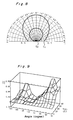
Fig. 8 is a graph showing a direction dependency of the light
intensity of LED. In this graph, a curve G1 illustrates a
direction dependency in each direction against the light
intensity of light Q1 having the maximum light intensity,
in which the intensity of light emitted in the lateral
direction spaced at 90 degrees from the upright direction
is only about 30% of that of upright direction. Further,
another curve G2 also illustrates a direction dependency
when the light intensity in the upright direction is reduced
to 50% by decreasing the voltage (current) applied to LED
in which the light intensity of lateral direction is only
about 10 %, not 30%, of that of the upright direction in curve
G1.
More disadvantageously, the light intensity
varies with the environmental temperature as well as
emitting direction. This is illustrated in a three
dimensional graph of Fig. 9 in which X, Y and Z axes
represent an angle of each direction from the upright
direction when the upright direction is zero degree,
environmental temperature (from 5 to 50 degrees centigrade)
and light intensity in each direction, respectively. In
this graph, the light intensity in each direction is
standardized by that of at 5 degrees centigrade. This shows
that the intensity of light changes with the environmental
temperature, but the increasing rate in one direction
differs from that of another direction. Namely, with the
increase of the environmental temperature, the ratio of
light intensity of between the monitoring light Q3' and
primary light Q1 varies depending upon the emitting angle.
It is believed that the direction dependency
of the light intensity is caused by a variation of density
of the current which flows in the light source, that may be
occurred from differences of electric properties of
assembled devices, connecting condition of electrodes of
the light emitting diode, and the like.
Thus, the light intensity of the primary light
Q1 emitted in the normal direction could not be determined
precisely by the detection of the monitoring light Q3'
emitted laterally, inhibiting the precise measurement of
the optical property of the sample.
Accordingly, it is an object of the invention
to provide a light emitting diode which is preferably used
in the optical apparatus.
It is another object of the invention to
provide an optical apparatus for use in an optical analyzer.
It is still another object of the invention
to provide an optical apparatus capable of measuring an
optical property such as reflectance or transmittancy of the
test sample with a great precision.
SUMMRY OF THE INVETNION
A light emitting diode of the invention
comprises a body made of resin pervious to light and a light
source having a semiconductor mounted in the body for
emitting a primary light. The body has a surface portion
where the primary light emitted from the light source is
divided into a first light for an optical analysis and a
second light for monitoring an intensity of the primary
light.
Preferably, the surface portion of the body
has small convex and concave portions for dividing the
primary light into the first and second lights.
More preferably, the surface portion is
slanted with respect to the primary light so that the first
light is a light which is reflected at the surface portion
and the second light is a light which is scattered at the
surface portion.
The surface potion may be a V-shaped recess
having first and second surfaces that intersect at a certain
angle so that the primary light is divided at an intersection
of the first and second surfaces into the first light
projected and then reflected on the first surface and the
second light projected and then reflected on the second
surface.
An optical apparatus of the invention
comprises a light emitting diode. The light emitting diode
includes a body made of resin which is pervious to light and
a light source having a semiconductor mounted in the body
for emitting a primary light. The body has a surface portion
where the primary light emitted from the light source is
divided into a first light which is intended to be
illuminated on a sample and a second light for monitoring
an intensity of the primary light. The apparatus further
comprises a first detector for detecting the first light
from the sample, a second detector for detecting the second
light and means for determining an optical property of the
sample from outputs of the first and second detectors.
The light emitting diode and the first and
second detectors may be integrally molded in a body of resin.
In this instance, preferably the resin of the molded body
is impervious to light and the molded body includes a first
passage for guiding the first light toward the sample,
second passage for guiding a light reflected from the sample
toward the first detector and a third passage for guiding
the second light toward the second detector.
According to the invention, the primary light
emitted from the light source is divided at the surface
portion of the body of the light emitting diode into first
and second lights. Subsequently, the first light is
reflected at or transmitted through the sample and then
detected by the first detector while the second light is
detected by the second detector. The output of the first
detector is used for determining the optical property of the
sample. The output of the second detector, on the other
hand, is used for determining the light intensity of the
primary light, thereby correcting the resultant optical
property. Therefore, the optical property of the sample can
be determined with a great precision even when the intensity
of the light emitted from the light source has varied due
to the changes of voltage or current applied with the light
source and/or the environmental temperature.
BRIEF DESCRIPTION OF THE DRAWINGS
Fig. 1 is a cross-sectional side elevational
view of an optical analyzer of the invention;
Fig. 2 is another cross-sectional side
elevational view of the optical analyzer of Fig. 1;
Fig. 3 is a side elevational view of a light
emitting diode of another embodiment according to the
invention;
Fig. 4 is a side elevational view of the light
emitting diode of another embodiment according to the
invention;
Fig. 5 is a side elevational view of the light
emitting diode of another embodiment according to the
invention;
Fig. 6 is a side elevational view of a
conventional optical analyzer;
Fig. 7 is a side elevational view of another
conventional optical analyzer;
Fig. 8 is a graph showing a directional
dependency of intensity of the light emitted from the light
emitting diode; and
Fig. 9 is a three dimensional graph showing
a temperature dependency of intensity of the light emitted
from the light emitting diode.
Corresponding reference characters indicate
corresponding parts throughout the several views of the
drawings.
DETAILED DESCRIPTION OF THE PREFERRED EMBODIMENT
With reference to the drawings, in particular
to Fig. 1, an optical analyzer of the invention generally
indicated reference numeral 100 includes a printed circuit
board 101 having an electric circuit (not shown) on both or
either side thereof. A light emitting diode (LED) generally
indicated by reference numeral 102 has a base 103, body 104
made of resin (e.g., epoxy resin) pervious to light, PN
junction semiconductor 105 integrally molded in the body 104
and capable of emitting light when it is applied with voltage
and a pair of terminals 106 electrically communicating the
semiconductor 105 with the circuit on the printed board 101.
The semiconductor 105 is so directed that a primary light
L having the maximum light intensity is emitted vertical to
and away from base 103.
The body 104 generally in the form of solid
cylinder is secured at its one end to the base 103. The other
end of body 104 remote from the base 103 is formed with a
surface 107 which is slanted at about 45 degrees against the
longitudinal axis of the body 104. Also, the body 104 is
formed at its peripheral portion adjacent the slanted
surface 107 with a domed surface portion or convex lens 108,
thereby most part of the primary light L emitted from the
semiconductor 105 is reflected at the slanted surface 107
and then transmitted substantially along a central axis of
the convex lens 108 toward a sample 109 (e.g., urine, blood,
or chemical compound) retained on a sample retaining plate
110 (e.g., PET (polyethylene terephthalate) plate) to be
releasably disposed above the circuit board 101. The body
104 is typically formed by molding and therefore undoubtedly
the slanted surface 107 has small or microscopic convex and
concave portions therein rather than perfect mirror,
thereby the primary light L emitted from the semiconductor
105 in part scatters out of the slanted surface 107. LED
102 thus constructed is so arranged that the reflected
primary light L1 travels in a direction away from the circuit
board 101 toward the sample 109.
A first optical sensor 111 having a pair of
terminals 112 is disposed above LED 102 so that it can detect
a part of light L1' of the primary light L which would be
reflected at the sample 109. Preferably, the first optical
sensor 111 is so oriented that it can receive the reflected
light L1' traveling in a direction which intersects with the
primary light L1 advancing to the sample 109 at an angle of
45 degrees. Also, a second optical sensor 113 having a pair
of terminals 114 is disposed to oppose the slanted surface
107 of LED 102 so that it can detect the scattered light L2
at the slanted surface 107. This arrangement ensures that
a ratio of light intensity of between the primary light and
the scattered light is independent of driving condition of
LED 102 and therefore the light intensity detected by the
optical sensor 111 can be corrected using the detected light
intensity of the scattered light. The optical sensors 111
and 113 are commercially available under the trade
designation PIN photodiode (SPS-503A1) from SANYO ELECTRIC
CO., Ltd. Also, the terminals 112 and 114 are secured on
the printed circuit board 101 and electrically communicated
with the circuit on the board 101.
Preferably, LED 102 and optical sensors 111
and 113 are integrally molded in a molded body 115 on the
circuit board 101 with a resin, such as ABS, which is
impervious to light. The molded body 115 includes therein
a first passage 116 which extends from the convex lens 108
to one or top surface 117 facing the sample retaining plate
110 and a second passage 118 which extends from the first
optical sensor 111 to the top surface 117 so that the primary
light L1 from the semiconductor 105 can travel through the
first passage 116 to illuminate the sample 109 on the sample
retaining plate 110 and then the reflected light L1' travels
to the first optical sensor 111. The molded body 115 also
includes a third passage 119 which extends from the slanted
surface 107 to the second optical sensor 113 so that the
scattered light L2 of the primary light can reach the second
optical sensor 113.
Preferably, the passages 117, 118 and 119 are
formed in the molded body 115 by arranging tubes
corresponding to respective passages in a mold prior to the
molding of body 115.
Preferably, openings of the first and second
passages 116 and 118, confronting the sample 109, are
covered with a transparent plate not shown to prevent
foreign matters from entering into the passages 116 and 118.
More preferably, a thermal sensor 120 is
integrally mounted in the molded body 115 for detecting a
temperature. The thermal sensor 120 includes a pair of
terminals 121 which is electrically connected with the
circuit on the board 101. It is to be understood that the
thermal sensor 120 may be disposed outside the molded body
115.
Also, mounted on the circuit board 101 is a
central processing unit (CPU) 122 which is electrically
connected with LED 102, first and second optical sensors 111
and 113 and thermal sensor 120.
Having described the general construction of
the optical analyzer 100, its operation will now be
described. Firstly, a reference plate (not shown) which
retains thereon a reference sample having a known
reflectance of, for example, 50% is so positioned that the
reference sample confronts the openings of the passages 116
and 118. CPU 122 instructs LED 102 to energize the
semiconductor 105 for emitting. The primary light L emitted
from the semiconductor 105 travels toward the slanted
surface 107 where the major part thereof reflects. The
reflected primary light L1 further travels through the
convex lens 108 and the passage 116 to reach the sample 109
on the sample retaining plate 110 where it reflects again.
Part of the second reflected primary light L1' travels into
the passage 118 to the first optical sensor 111 which detects
the intensity of second reflected primary light L1'. The
optical sensor 111 outputs a signal corresponding to the
detected light intensity to CPU 122. The primary light L
from the semiconductor 105 scatters at the slanted surface
107 due to the existence of the microscopic convex and
concave portions. The scattered light L2 travels through
the passage 119 to reach the second optical sensor 113. The
optical sensor 113 outputs a signal corresponding to the
intensity of the detected scattered light L2 to CPU 122. In
addition, the thermal sensor 120 outputs a signal
corresponding to the temperature of the molded body 115 to
CPU 122. With the signals from the optical sensors 111 and
113, CPU 122 corrects data stored therein so that the
calculated reflectance of the reference plate will be 50%.
Secondly, the reference plate is replaced by
the sample retaining plate 110 retaining a test sample 109
so that the test sample 109 confronts the openings of the
passages 116 and 118. CPU 122 performs the same process to
determine the reflectance of the sample 109 from the light
intensity detected by the first optical sensor 111 using the
light intensity detected by the second optical sensor 113
according to the following equation:
RSAM= RREF · [VSAM (1) · VREF(2)] / [VSAM(2) · VREF(1)]
where
- RSAM :
- Reflectance of test sample
- VREF(1):
- Output voltage of first optical sensor for
reference sample
- VREF(2):
- Output voltage of second optical sensor for
reference sample
- VSAM(1):
- Output voltage of first optical sensor for
test sample
- VSAM(2):
- Output voltage of second optical sensor for
test sample
Specifically, assume that the reference plate
has a reflectance RREF of 50% and output voltages VREF(1) and
VREF(2) of the first and second optical sensors 111 and 113
are 44 milli-volts and of 4.2 milli-volts, respectively.
Also assume that, for the test sample on the sample retaining
plate replaced by the reference plate, outputs voltages VSAM
(1) and VSAM (2)of the first and second optical sensors 111
and 113 are 12 milli-volts and 4.2 milli-volts. In this
instance, the reflectance of the sample can be obtained as
follows:
RSAM= RREF · VSAM (1) / VREF(1)
= 50 · 12/44
= 13.6 %
Alternately, if the output voltage VSAM (2) is
decreased to 4.0 milli-volts, the reflectance of the sample
will be obtained as follows:
RSAM= RREF · [VSAM (1) · VREF(2)] / [VSAM(2) · VREF(1)]
= 50 · [12 · 4.2] / [44 · 4.0]
= 14.3 %
The invention is not limited to the embodiment
described and it may be modified in different manners. For
example, as shown in Fig. 3, LED 130 may have a conventional
configuration. In this instance, the body 131 of LED 130
is formed at its distal end away from the base 132 with a
domed surface 133. Also, a central portion 134 of the domed
surface 133 is formed with small or microscopic convex and
concave portions by a suitable manner such as sandblast.
Instead, the convex and concave portions may be formed at
molding of the body 131 by providing corresponding convex
and concave portions on an inner surface of the mold. With
this LED 130, the primary light L emitted from the
semiconductor 135 scatters in part at the central portion
134. Therefore, by detecting the scattered light L2 using
the optical sensor, the light intensity of the primary light
can be corrected.
Typically, the molded surface includes
microscopic convex and concave potions. Therefore, it is
not necessary to form such small convex and concave portions
by the above described techniques. In this event, a feeble
scattering light is generated when the primary light
transmits the surface of the LED body. Therefore, by
detecting the feeble scattering light by the optical sensor,
the light intensity of the primary light can be corrected.
Fig. 4 shows another embodiment of the
invention. In this embodiment, the body 141 of LED 140 has
a V-shaped recess 142 with its bottom portion confronting
the semiconductor 143. Preferably, two surfaces 144 and 145
of the V-shaped recess 142 are spaced apart from each other
at 90 degrees. In this event, the primary light emitted from
the semiconductor 143 is illuminated at the bottom portion
of the V-shaped recess 142 where it is divided into two, one
light L1 reflected at the surface 144 and then being
transmitted in one direction for illumination of test sample
and the other light reflected at the surface 145 and then
transmitted in the opposite direction for monitoring.
Fig. 5 shows still another embodiment of the
LED body 151 in which the domed surface or convex lens is
eliminated therefrom.
Although the optical analyzer is designed to
determine the reflectance of the sample, it may be modified
to determine a transmittancy of light.
In view of the above, it will be seen that the
several objects of the invention are achieved and other
advantages results attained.
As various changes could be made in the above
constructions without departing from the scope of the
invention, it is intended that all matter contained in the
above description or shown in the accompanying drawings
shall be interpreted as illustrative and not in a limiting
sense.