EP0823115B1 - Reference for cmos memory cell having pmos and nmos transistors with a common floating gate - Google Patents
Reference for cmos memory cell having pmos and nmos transistors with a common floating gate Download PDFInfo
- Publication number
- EP0823115B1 EP0823115B1 EP96909868A EP96909868A EP0823115B1 EP 0823115 B1 EP0823115 B1 EP 0823115B1 EP 96909868 A EP96909868 A EP 96909868A EP 96909868 A EP96909868 A EP 96909868A EP 0823115 B1 EP0823115 B1 EP 0823115B1
- Authority
- EP
- European Patent Office
- Prior art keywords
- voltage
- pmos
- source
- memory cell
- transistor
- Prior art date
- Legal status (The legal status is an assumption and is not a legal conclusion. Google has not performed a legal analysis and makes no representation as to the accuracy of the status listed.)
- Expired - Lifetime
Links
Images

Classifications
-
- G—PHYSICS
- G11—INFORMATION STORAGE
- G11C—STATIC STORES
- G11C5/00—Details of stores covered by group G11C11/00
- G11C5/14—Power supply arrangements, e.g. power down, chip selection or deselection, layout of wirings or power grids, or multiple supply levels
- G11C5/147—Voltage reference generators, voltage or current regulators; Internally lowered supply levels; Compensation for voltage drops
-
- G—PHYSICS
- G05—CONTROLLING; REGULATING
- G05F—SYSTEMS FOR REGULATING ELECTRIC OR MAGNETIC VARIABLES
- G05F3/00—Non-retroactive systems for regulating electric variables by using an uncontrolled element, or an uncontrolled combination of elements, such element or such combination having self-regulating properties
- G05F3/02—Regulating voltage or current
- G05F3/08—Regulating voltage or current wherein the variable is dc
- G05F3/10—Regulating voltage or current wherein the variable is dc using uncontrolled devices with non-linear characteristics
- G05F3/16—Regulating voltage or current wherein the variable is dc using uncontrolled devices with non-linear characteristics being semiconductor devices
- G05F3/20—Regulating voltage or current wherein the variable is dc using uncontrolled devices with non-linear characteristics being semiconductor devices using diode- transistor combinations
- G05F3/24—Regulating voltage or current wherein the variable is dc using uncontrolled devices with non-linear characteristics being semiconductor devices using diode- transistor combinations wherein the transistors are of the field-effect type only
- G05F3/242—Regulating voltage or current wherein the variable is dc using uncontrolled devices with non-linear characteristics being semiconductor devices using diode- transistor combinations wherein the transistors are of the field-effect type only with compensation for device parameters, e.g. channel width modulation, threshold voltage, processing, or external variations, e.g. temperature, loading, supply voltage
- G05F3/247—Regulating voltage or current wherein the variable is dc using uncontrolled devices with non-linear characteristics being semiconductor devices using diode- transistor combinations wherein the transistors are of the field-effect type only with compensation for device parameters, e.g. channel width modulation, threshold voltage, processing, or external variations, e.g. temperature, loading, supply voltage producing a voltage or current as a predetermined function of the supply voltage
Definitions
- the present invention relates to CMOS memory cells having PMOS and NMOS transistors with a common floating gate. More particularly, the present invention relates to a voltage reference for supplying voltage to such CMOS memory cells during read operations.
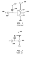
- Fig. 1 illustrates the configuration of a CMOS memory cell 100 having a PMOS transistor 102 and an NMOS transistor 104 with a common floating gate. Drains of transistors 102 and 104 are further connected together to form an output node 106. Bias voltage is provided to the common floating gate through capacitors 108 and 109 at nodes 118 and 119.
- CMOS memory cell is disclosed in U.S. Patent No. 5,272,368 entitled "Complementary Low Power Non-Volatile Reconfigurable EECELL," and in U.S. Patent No. 4,885,719 entitled “Improved Logic Cell Array Using CMOS E 2 PROM Cells.”
- the CMOS memory cell 100 is typically included in an array of cells on an integrated circuit chip. Bias voltage is typically provided to the source of the PMOS transistors in the CMOS memory cells, such as transistor 102, from an external source through the chip's Vcc pin. The source of the NMOS transistors in the CMOS memory cells, such as transistor 104, are provided through the chip's ground or Vss pin.
- the CMOS memory cell 100 is advantageous because it enables zero power operation, zero power operation indicating that a component does not continually draw power when the component is not changing states. For instance, with an appropriate voltage applied to the floating gate, transistor 102 will conduct and transistor 104 will not conduct. Current will then be provided from Vcc through transistor 102 to the output node 106 until the output node 106 is charged up to Vcc. In this configuration, no current will be provided through transistor 104 to Vss. Further, with another voltage applied to the floating gate, transistor 104 will conduct while transistor 102 does not. Node 106 will then discharge to Vss. No additional current will be provided through transistor 102 from Vcc to Vss.
- CMOS memory cell design of Fig. 1 enables zero power operation as described, the CMOS array cell 100 is not typically included in an array of memory cells on an integrated circuit chip. Instead a memory cell including a single NMOS transistor is utilized, such as the memory cell 200 of Fig. 2.
- the memory cell 200 of Fig. 2 includes a single NMOS transistor 202 having a floating gate. Voltage is provided to the floating gate of transistor 202 through capacitors 208 and 209, similar to the manner voltage is provided to the common floating gate of transistors 102 and 104 in Fig. 1.
- the memory cell 200 does not directly provide zero power operation as does the memory cell 100 shown in Fig. 1. For instance, with an appropriate charge applied to the floating gate of transistor 202 to enable it to conduct, transistor 202 will continuously conduct power from Vcc to Vss.
- Including a PMOS transistor in a memory cell, as in the memory cell of Fig. 1, has previously not been considered practical for replacing the design of Fig. 2 because the threshold of the PMOS transistor is referenced to Vcc rather than to Vss as with an NMOS transistor.
- threshold voltage is the gate to source voltage enabling a transistor to turn on.
- Vcc voltage on the floating gate of a CMOS cell must be varied to assure its PMOS transistor is turned off.
- Table I shows the state of NMOS and PMOS transistors with varied floating gate (F.G.) voltages, as listed.
- Vcc is varied from 3.0V to 4.0V.
- the magnitude of the threshold voltage (Vtp) for the PMOS transistor 102 is 1.5V
- the magnitude of the threshold voltage (Vtn) for the NMOS transistor 104 is 1.5V.
- F.G. 0.5 1.5 2.0 2.5 3.0 3.5 n-chan. off off on on on on p-chan. on on off off off off off off off off off off
- CMOS configuration shown in Fig. 1, which is capable of providing zero power operation, as opposed to the memory cell design of Fig. 2.
- EP - A - 431 911 discloses a memory cell (see Figure 3) having PMOS and NMOS transistors having common floating gates and a common drain.
- a voltage generator (14) is connected to Vcc and supplies an internal voltage VSE to the memory cell, VSE being less than Vcc.
- a voltage generator (3) comprising a voltage reference circuit (fig.24) having a PMOS transistor (TPR) and an NMOS transistor (TNR) serially connected between first and second voltage supplies, said PMOS and NMOS transistors having drains connected in common and having a common gate connected to the common drains.
- the present invention provides an integrated circuit comprising:
- CMOS memory cells may be utilized on an integrated circuit chip to provide zero power operation by providing a source voltage to the PMOS transistors of the memory cells, the voltage remaining stable with variations in Vcc.
- the present invention may provide voltages to the CMOS memory cells during read to enable a minimum amount of charge to be added or removed from floating gates to turn the cells on or off.
- the present invention utilizes a conventional voltage reference providing a voltage more stable than Vcc, wherein charge on the floating gate of CMOS memory cells can be provided to assure the PMOS transistor of a CMOS memory cell remains off for the maximum range of the reference.
- a voltage reference is configured to enable a minimum amount of charge to be added or removed from a floating gate to turn a CMOS cell on or off.
- the voltage reference includes a PMOS transistor and an NMOS transistor with a common floating gate.
- the reference is provided on a single integrated circuit with the CMOS memory cells to which the reference supplies voltage.
- the common floating gate of the PMOS and NMOS transistors of the reference are coupled to their drains.
- the source of the NMOS transistor of the reference is connected to Vss.
- the reference further includes a weak current source coupled to supply current to the source of the PMOS transistor of the reference.
- the weak current source enables the PMOS and NMOS transistors to barely turn on so that the voltage at the drain of the NMOS transistor is substantially equal to the magnitude of the threshold of the NMOS transistor (Vtn) and the voltage at the source of the PMOS transistor is substantially equal to the magnitude of the threshold of the PMOS transistor (Vtp) plus Vtn.
- the source of the PMOS transistor of the reference is coupled to the source of each PMOS transistor of the CMOS memory cells. Because the thresholds of PMOS and NMOS transistors of the CMOS memory cells remain constant on a single integrated circuit, the voltage provided by the reference to the source of the PMOS transistors of each CMOS memory cell will be substantially equal to the sum of the magnitude of the thresholds of its PMOS transistor and NMOS transistor.
- a reference voltage is further provided from the drain of the NMOS transistor of the reference to the gate of one or more capacitors to which the floating gate voltage of each CMOS memory cell is referenced.
- Vtn + Vtp to the source of the PMOS transistor of a CMOS memory cell
- Vtn + Vtp less than Vcc
- an additional CMOS circuit stage connected to the CMOS memory cell output which has Vcc applied to the source of its PMOS transistor will continually burn power.
- the present invention utilizes cell implants in the PMOS and NMOS transistors of the CMOS memory cells and the reference to assure Vtn + Vtp is equal to or greater than Vcc. Additionally, to assure the sources of the PMOS transistors of the CMOS memory cells maintain a value equal to or greater than Vcc, voltage applied to the source of the PMOS transistor of the reference is boosted above Vcc.
- Fig. 3 illustrates the configuration of the present invention which includes a reference 300 connected to a CMOS memory cell 100 as shown in Fig. 1.
- voltage reference 300 receives a supply voltage from the Vcc pin of a chip and provides a more stabilized voltage to a CMOS memory cell 100 during read operations.
- One output, Vpref, of the reference 300 is supplied to the source of the PMOS transistor 102 of the CMOS memory cell 100.
- a second output, Vacg, of the reference 300 of Fig. 3 may also be provided as an array control gate reference to one or both capacitors 108 and 109 through nodes 118 and 119.
- the Vacg voltage output from reference 300 enables less charge to be provided to the floating gate of the CMOS memory cell to assure the memory cell remains in a particular state.
- a voltage Vcc/2 is supplied to the gate of capacitors 108 and 109 as disclosed in U.S. Patent No. 5,272,368, previously referenced.
- Voltage on the floating gate of cell 100 is determined with reference to voltage on the inputs 118 and 119 to capacitors 108 and 109, as well as to the voltage on the sources of the NMOS and PMOS transistors.
- Vcc/2 applied to the inputs 118 and 119 of capacitors 108 and 109
- the floating gate voltage value will vary as Vss changes, dictating that a greater range of charge must be added or removed from the floating gate to assure that transistors in the CMOS cell remains either on or off.
- the reference constitutes a conventional voltage reference operating such that with variations in the supply voltage Vcc, the reference will provide a more stable voltage so that charge can be maintained on the floating gate of a CMOS memory cell sufficient to assure the CMOS memory cell remains either on or off.
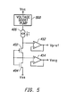
- Fig. 4 shows another embodiment of the reference of the present invention.
- the voltage reference includes a PMOS transistor 402 and an NMOS transistor 404 with a common floating gate.
- the common floating gate of the PMOS transistor 402 and NMOS transistor 404 of the reference is coupled to the drain of NMOS transistor 404. Drains of transistors 402 and 404 are further coupled together.
- the source of the NMOS transistor of the reference is connected to Vss.
- the reference further includes a weak current source 406 coupled to supply current to the source of the PMOS transistor 402.
- the weak current source 406 supplies a low current, for example 0.1 ⁇ amps, to enable the PMOS transistor 402 and NMOS transistor 404 to barely turn on. With transistors 402 and 404 barely on, voltage at the drain of the NMOS transistor 404 is substantially equal to the magnitude of the threshold (Vtn) of the NMOS transistor 404 and the voltage at the source of the PMOS transistor 402 is substantially equal to the magnitude of the threshold (Vtp) of the PMOS transistor 402 plus Vtn.
- the source of the PMOS transistor 402 of the reference 400 is coupled to the source of each PMOS transistor of the CMOS memory cells. Because a large number of memory cells may provide a capacitive load adversely affecting the voltage at the source of the PMOS transistor 402, a voltage follower buffer 412 can be provided to couple the source of transistor 402 to the source of PMOS transistors of the CMOS memory cells.
- a reference voltage is further coupled from the drain of the NMOS transistor 404 to provide the Vacg reference output of Fig. 3 to inputs of capacitors connected to the floating gates of CMOS memory cells. Because a large number of memory cells may provide a capacitive load adversely affecting the voltage at the source of the NMOS transistor 404, a voltage follower buffer 414 can be provided to couple the drain of transistor 404 to capacitors of the CMOS memory cells.
- Transistors 402 and 404 are provided on a single integrated circuit with the CMOS memory cells to which the voltage reference supplies bias voltage. Because the thresholds of PMOS and NMOS transistors remain constant on a single integrated circuit, the voltage provided from the source of PMOS transistor 402 will be substantially equal to the sum of the thresholds of any similarly configured PMOS transistor and NMOS transistor on the same integrated circuit. Further, the voltage provided from the drain of NMOS transistor 404 will be substantially equal to the threshold of any similarly configured NMOS transistor on the same integrated circuit.
- the present invention first utilizes cell implants in the PMOS and NMOS transistors of the reference and the CMOS memory cells on the integrated circuit.
- the cell implants constitute additional ion implantation in the channel between the source and drain of the PMOS and NMOS transistors.
- the cell implants are added to an extent to assure Vtn + Vtp of the PMOS and NMOS transistors is equal to or greater than Vcc.
- a voltage boost pump 500 is added to the circuitry of Fig. 4 to boost voltage above Vcc which is supplied to the source of the PMOS transistor of the reference. With the output of the CMOS memory cells providing a voltage range equal to or greater than Vcc, no current leakage will occur in subsequent CMOS stages enabling zero power operation throughout an integrated circuit.
Description
| (Vcc=3.0V, Vtp=1.5V, Vtn=1.5V) | |||||||
| F.G.= | 0.5 | 1.5 | 2.5 | ||||
| n-chan. | off | off | on | ||||
| p-chan. | on | off | off | ||||
| (Vcc=4.0V, Vtp=1.5V, Vtn=1.5V) | |||||||
| F.G.= | 0.5 | 1.5 | 2.0 | 2.5 | 3.0 | 3.5 | |
| n-chan. | off | off | on | on | on | on | |
| p-chan. | on | on | on | off | off | off |
- a source of the PMOS transistor of the memory cell being coupled to a source of the PMOS transistor of the reference circuit and to a current supply means, cf p.11 the voltage appearing at the source of the PMOS transistor of the reference circuit being substantially equal to a sum of magnitudes of thresholds of the NMOS and PMOS transistors of the reference circuit.
Claims (7)
- An integrated circuit comprising:characterised in that said voltage generating circuit comprises a voltage reference circuit (400) comprising a PMOS transistor (402) and an NMOS transistor (404) having drains connected in common and having a common gate connected to the common drains; anda voltage generating circuit (400);a memory cell (100) comprising a PMOS transistor (102) and an NMOS transistor (104) with a common floating gate;a source of the PMOS transistor of the memory cell being coupled to a source of the PMOS transistor of the reference circuit and to a current supply means (406), the current applied by said current supply means being such to barely forming on said PMOS and NMOS transistors of said reference circuit such that the voltage appearing at the source of the PMOS transistor of the reference circuit being substantially equal to a sum of magnitudes of thresholds of the NMOS and PMOS transistors of the reference circuit.
- The integrated circuit of Claim 1 wherein said current supply means is a weak current source (406) having an input coupled to a voltage (Vcc) from a voltage supply pin, and an output applying current to the source of the PMOS transistor of the reference circuit.
- The integrated circuit of Claim 1, wherein the memory cell further comprises a capacitor (108. 109) having a first end connected to the common floating gate and a second end coupled to the drain of the NMOS transistor of the reference circuit.
- The integrated circuit of Claim 3 wherein the reference circuit comprises:a first voltage follower buffer (412) coupling the source of the PMOS transistor of the reference circuit to the source of the PMOS transistor of the memory cell.
- The integrated circuit of Claim 4 wherein the reference circuit further comprises:a second voltage follower buffer (414) coupling the drain of the NMOS transistor of the reference circuit to the second end of the capacitor of the memory cell.
- The integrated circuit of any of Claims 2 to 5 wherein the PMOS and NMOS transistors of the reference circuit include ion-implanted cell regions so that the sum of the magnitude of the thresholds of the PMOS and NMOS transistors of the reference circuit are substantially equal to or greater than the voltage (Vcc) received from the voltage supply pin.
- The integrated circuit of Claim 6 further comprising a voltage boost pump (500) for coupling the voltage (Vcc) from the voltage supply pin to the input of the weak current source the voltage boost pump (500) providing a boosted voltage higher than the voltage (Vcc) to the input of the weak current source.
Applications Claiming Priority (3)
| Application Number | Priority Date | Filing Date | Title |
|---|---|---|---|
| US42674195A | 1995-04-21 | 1995-04-21 | |
| PCT/US1996/004124 WO1996033496A1 (en) | 1995-04-21 | 1996-03-26 | Reference for cmos memory cell having pmos and nmos transistors with a common floating gate |
| US426741 | 2003-04-30 |
Publications (2)
| Publication Number | Publication Date |
|---|---|
| EP0823115A1 EP0823115A1 (en) | 1998-02-11 |
| EP0823115B1 true EP0823115B1 (en) | 1999-08-25 |
Family
ID=23692021
Family Applications (1)
| Application Number | Title | Priority Date | Filing Date |
|---|---|---|---|
| EP96909868A Expired - Lifetime EP0823115B1 (en) | 1995-04-21 | 1996-03-26 | Reference for cmos memory cell having pmos and nmos transistors with a common floating gate |
Country Status (4)
| Country | Link |
|---|---|
| US (1) | US5796295A (en) |
| EP (1) | EP0823115B1 (en) |
| TW (1) | TW314627B (en) |
| WO (1) | WO1996033496A1 (en) |
Families Citing this family (13)
| Publication number | Priority date | Publication date | Assignee | Title |
|---|---|---|---|---|
| US6597619B2 (en) * | 2001-01-12 | 2003-07-22 | Micron Technology, Inc. | Actively driven VREF for input buffer noise immunity |
| US6731163B2 (en) | 2002-03-08 | 2004-05-04 | Texas Instruments Incorporated | Miller de-compensation for differential input, differential output amplifier |
| JP4368223B2 (en) * | 2003-03-26 | 2009-11-18 | 三洋電機株式会社 | Bias voltage generation circuit and amplifier circuit |
| CN103348574B (en) * | 2010-12-03 | 2016-03-02 | 马维尔国际贸易有限公司 | The insensitive inverter of flow-route and temperature |
| US8665007B2 (en) | 2011-06-10 | 2014-03-04 | Cypress Semiconductor Corporation | Dynamic power clamp for RFID power control |
| US8841890B2 (en) | 2011-06-10 | 2014-09-23 | Cypress Semiconductor Corporation | Shunt regulator circuit having a split output |
| US8823267B2 (en) | 2011-06-10 | 2014-09-02 | Cypress Semiconductor Corporation | Bandgap ready circuit |
| US8729874B2 (en) | 2011-06-10 | 2014-05-20 | Cypress Semiconductor Corporation | Generation of voltage supply for low power digital circuit operation |
| US8729960B2 (en) | 2011-06-10 | 2014-05-20 | Cypress Semiconductor Corporation | Dynamic adjusting RFID demodulation circuit |
| US8669801B2 (en) | 2011-06-10 | 2014-03-11 | Cypress Semiconductor Corporation | Analog delay cells for the power supply of an RFID tag |
| US8584959B2 (en) | 2011-06-10 | 2013-11-19 | Cypress Semiconductor Corp. | Power-on sequencing for an RFID tag |
| US9361986B2 (en) * | 2011-09-19 | 2016-06-07 | Sandisk Technologies Inc. | High endurance non-volatile storage |
| US10581645B1 (en) * | 2019-05-30 | 2020-03-03 | Nvidia Corp. | Dual-rail transceiver with improved signal-to-noise ratio for differential high-speed links |
Family Cites Families (10)
| Publication number | Priority date | Publication date | Assignee | Title |
|---|---|---|---|---|
| US5086238A (en) * | 1985-07-22 | 1992-02-04 | Hitachi, Ltd. | Semiconductor supply incorporating internal power supply for compensating for deviation in operating condition and fabrication process conditions |
| JP2501590B2 (en) * | 1987-07-29 | 1996-05-29 | 沖電気工業株式会社 | Driving circuit for semiconductor device |
| US4885719A (en) * | 1987-08-19 | 1989-12-05 | Ict International Cmos Technology, Inc. | Improved logic cell array using CMOS E2 PROM cells |
| KR910003604B1 (en) * | 1988-04-30 | 1991-06-07 | 삼성전자 주식회사 | Reference voltage generating circuit using charging-up and discharging-up circuit |
| FR2650109B1 (en) * | 1989-07-20 | 1993-04-02 | Gemplus Card Int | INTEGRATED MOS CIRCUIT WITH ADJUSTABLE THRESHOLD VOLTAGE |
| JPH03179780A (en) * | 1989-12-07 | 1991-08-05 | Fujitsu Ltd | Semiconductor device |
| US4975883A (en) * | 1990-03-29 | 1990-12-04 | Intel Corporation | Method and apparatus for preventing the erasure and programming of a nonvolatile memory |
| US5272368A (en) * | 1991-05-10 | 1993-12-21 | Altera Corporation | Complementary low power non-volatile reconfigurable EEcell |
| KR940017214A (en) * | 1992-12-24 | 1994-07-26 | 가나이 쓰토무 | Reference voltage generator |
| US5434534A (en) * | 1993-11-29 | 1995-07-18 | Intel Corporation | CMOS voltage reference circuit |
-
1996
- 1996-03-26 WO PCT/US1996/004124 patent/WO1996033496A1/en active IP Right Grant
- 1996-03-26 EP EP96909868A patent/EP0823115B1/en not_active Expired - Lifetime
- 1996-04-01 TW TW085103782A patent/TW314627B/zh active
- 1996-06-21 US US08/668,141 patent/US5796295A/en not_active Expired - Fee Related
Also Published As
| Publication number | Publication date |
|---|---|
| EP0823115A1 (en) | 1998-02-11 |
| TW314627B (en) | 1997-09-01 |
| US5796295A (en) | 1998-08-18 |
| WO1996033496A1 (en) | 1996-10-24 |
Similar Documents
| Publication | Publication Date | Title |
|---|---|---|
| US6094095A (en) | Efficient pump for generating voltages above and/or below operating voltages | |
| US6133777A (en) | Selector circuit for the switching over of analog signals with amplitudes greater than that of the supply voltage | |
| US6023187A (en) | Voltage pump for integrated circuit and operating method thereof | |
| EP0389566B1 (en) | Improved low power dual-mode cmos bias voltage generator | |
| EP0823115B1 (en) | Reference for cmos memory cell having pmos and nmos transistors with a common floating gate | |
| KR970004464B1 (en) | Efficient negative charge pump | |
| US5872476A (en) | Level converter circuit generating a plurality of positive/negative voltages | |
| US20070121358A1 (en) | Semiconductor integrated circuit | |
| US6198340B1 (en) | High efficiency CMOS pump circuit | |
| JPS6020394A (en) | Power source switching circuit | |
| EP0945985B1 (en) | Semiconductor device comprising a level shifting circuit | |
| US20080284504A1 (en) | Semiconductor integrated circuit | |
| EP0594230B1 (en) | High efficiency n-channel charge pump | |
| US4638182A (en) | High-level CMOS driver circuit | |
| US6385099B1 (en) | Reducing level shifter standby power consumption | |
| US20020085413A1 (en) | Sample and hold voltage reference source | |
| US6208539B1 (en) | Two-phase clock charge pump with power regulation | |
| US6747492B2 (en) | Power-on reset circuit with current shut-off and semiconductor device including the same | |
| US6617916B1 (en) | Semiconductor integrated circuit | |
| US5629843A (en) | Self compensating clamp circuit and method for limiting a potential at a pump circuit node | |
| US7315196B2 (en) | Voltage generating circuit that produces internal supply voltage from external supply voltage | |
| EP0735540A2 (en) | Low power sense amplifier for gain memory cells | |
| KR0149224B1 (en) | Internal pumping voltage circuit of semiconductor | |
| US6512698B2 (en) | Semiconductor device | |
| US6861872B2 (en) | Voltage down converter for low voltage operation |
Legal Events
| Date | Code | Title | Description |
|---|---|---|---|
| PUAI | Public reference made under article 153(3) epc to a published international application that has entered the european phase |
Free format text: ORIGINAL CODE: 0009012 |
|
| 17P | Request for examination filed |
Effective date: 19970825 |
|
| AK | Designated contracting states |
Kind code of ref document: A1 Designated state(s): GB IE |
|
| GRAG | Despatch of communication of intention to grant |
Free format text: ORIGINAL CODE: EPIDOS AGRA |
|
| 17Q | First examination report despatched |
Effective date: 19981124 |
|
| GRAG | Despatch of communication of intention to grant |
Free format text: ORIGINAL CODE: EPIDOS AGRA |
|
| GRAH | Despatch of communication of intention to grant a patent |
Free format text: ORIGINAL CODE: EPIDOS IGRA |
|
| GRAH | Despatch of communication of intention to grant a patent |
Free format text: ORIGINAL CODE: EPIDOS IGRA |
|
| GRAA | (expected) grant |
Free format text: ORIGINAL CODE: 0009210 |
|
| AK | Designated contracting states |
Kind code of ref document: B1 Designated state(s): GB IE |
|
| REG | Reference to a national code |
Ref country code: IE Ref legal event code: FG4D |
|
| PLBE | No opposition filed within time limit |
Free format text: ORIGINAL CODE: 0009261 |
|
| STAA | Information on the status of an ep patent application or granted ep patent |
Free format text: STATUS: NO OPPOSITION FILED WITHIN TIME LIMIT |
|
| 26N | No opposition filed | ||
| PGFP | Annual fee paid to national office [announced via postgrant information from national office to epo] |
Ref country code: IE Payment date: 20010430 Year of fee payment: 6 |
|
| REG | Reference to a national code |
Ref country code: GB Ref legal event code: IF02 |
|
| PG25 | Lapsed in a contracting state [announced via postgrant information from national office to epo] |
Ref country code: IE Free format text: LAPSE BECAUSE OF NON-PAYMENT OF DUE FEES Effective date: 20020326 |
|
| REG | Reference to a national code |
Ref country code: IE Ref legal event code: MM4A |
|
| REG | Reference to a national code |
Ref country code: GB Ref legal event code: 732E |
|
| PGFP | Annual fee paid to national office [announced via postgrant information from national office to epo] |
Ref country code: GB Payment date: 20070321 Year of fee payment: 12 |
|
| GBPC | Gb: european patent ceased through non-payment of renewal fee |
Effective date: 20080326 |
|
| PG25 | Lapsed in a contracting state [announced via postgrant information from national office to epo] |
Ref country code: GB Free format text: LAPSE BECAUSE OF NON-PAYMENT OF DUE FEES Effective date: 20080326 |