EP0822664A2 - System and method for synchronising data - Google Patents
System and method for synchronising data Download PDFInfo
- Publication number
- EP0822664A2 EP0822664A2 EP97305794A EP97305794A EP0822664A2 EP 0822664 A2 EP0822664 A2 EP 0822664A2 EP 97305794 A EP97305794 A EP 97305794A EP 97305794 A EP97305794 A EP 97305794A EP 0822664 A2 EP0822664 A2 EP 0822664A2
- Authority
- EP
- European Patent Office
- Prior art keywords
- pll
- charge pump
- data
- coupled
- vco
- Prior art date
- Legal status (The legal status is an assumption and is not a legal conclusion. Google has not performed a legal analysis and makes no representation as to the accuracy of the status listed.)
- Granted
Links
- 238000000034 method Methods 0.000 title claims description 23
- 230000003111 delayed effect Effects 0.000 claims description 2
- 229920000729 poly(L-lysine) polymer Polymers 0.000 abstract description 17
- 230000009977 dual effect Effects 0.000 abstract description 7
- 238000010586 diagram Methods 0.000 description 10
- 230000003287 optical effect Effects 0.000 description 9
- 101100082028 Arabidopsis thaliana PLL2 gene Proteins 0.000 description 8
- 230000000630 rising effect Effects 0.000 description 7
- 230000001360 synchronised effect Effects 0.000 description 6
- 101100350613 Arabidopsis thaliana PLL1 gene Proteins 0.000 description 5
- 102100020802 D(1A) dopamine receptor Human genes 0.000 description 5
- 101000931925 Homo sapiens D(1A) dopamine receptor Proteins 0.000 description 5
- 238000001514 detection method Methods 0.000 description 5
- 102100020756 D(2) dopamine receptor Human genes 0.000 description 4
- 101000931901 Homo sapiens D(2) dopamine receptor Proteins 0.000 description 4
- 239000003990 capacitor Substances 0.000 description 4
- 230000001419 dependent effect Effects 0.000 description 4
- 230000004907 flux Effects 0.000 description 3
- 101100350628 Arabidopsis thaliana PLL3 gene Proteins 0.000 description 2
- 101000631899 Homo sapiens Ribosome maturation protein SBDS Proteins 0.000 description 2
- 102100028750 Ribosome maturation protein SBDS Human genes 0.000 description 2
- 238000011084 recovery Methods 0.000 description 2
- 101100417903 Arabidopsis thaliana RRC1 gene Proteins 0.000 description 1
- XUIMIQQOPSSXEZ-UHFFFAOYSA-N Silicon Chemical compound [Si] XUIMIQQOPSSXEZ-UHFFFAOYSA-N 0.000 description 1
- 238000013500 data storage Methods 0.000 description 1
- 230000007423 decrease Effects 0.000 description 1
- 230000007547 defect Effects 0.000 description 1
- 238000005516 engineering process Methods 0.000 description 1
- 238000007667 floating Methods 0.000 description 1
- 238000002955 isolation Methods 0.000 description 1
- 230000005381 magnetic domain Effects 0.000 description 1
- 239000006249 magnetic particle Substances 0.000 description 1
- 230000008520 organization Effects 0.000 description 1
- 230000010287 polarization Effects 0.000 description 1
- 229910052710 silicon Inorganic materials 0.000 description 1
- 239000010703 silicon Substances 0.000 description 1
Images





Classifications
-
- G—PHYSICS
- G11—INFORMATION STORAGE
- G11B—INFORMATION STORAGE BASED ON RELATIVE MOVEMENT BETWEEN RECORD CARRIER AND TRANSDUCER
- G11B20/00—Signal processing not specific to the method of recording or reproducing; Circuits therefor
- G11B20/10—Digital recording or reproducing
- G11B20/10009—Improvement or modification of read or write signals
- G11B20/10222—Improvement or modification of read or write signals clock-related aspects, e.g. phase or frequency adjustment or bit synchronisation
- G11B20/1024—Improvement or modification of read or write signals clock-related aspects, e.g. phase or frequency adjustment or bit synchronisation wherein a phase-locked loop [PLL] is used
-
- H—ELECTRICITY
- H03—ELECTRONIC CIRCUITRY
- H03L—AUTOMATIC CONTROL, STARTING, SYNCHRONISATION OR STABILISATION OF GENERATORS OF ELECTRONIC OSCILLATIONS OR PULSES
- H03L7/00—Automatic control of frequency or phase; Synchronisation
- H03L7/06—Automatic control of frequency or phase; Synchronisation using a reference signal applied to a frequency- or phase-locked loop
- H03L7/08—Details of the phase-locked loop
- H03L7/0805—Details of the phase-locked loop the loop being adapted to provide an additional control signal for use outside the loop
-
- G—PHYSICS
- G11—INFORMATION STORAGE
- G11B—INFORMATION STORAGE BASED ON RELATIVE MOVEMENT BETWEEN RECORD CARRIER AND TRANSDUCER
- G11B20/00—Signal processing not specific to the method of recording or reproducing; Circuits therefor
- G11B20/10—Digital recording or reproducing
- G11B20/14—Digital recording or reproducing using self-clocking codes
- G11B20/1403—Digital recording or reproducing using self-clocking codes characterised by the use of two levels
-
- H—ELECTRICITY
- H03—ELECTRONIC CIRCUITRY
- H03L—AUTOMATIC CONTROL, STARTING, SYNCHRONISATION OR STABILISATION OF GENERATORS OF ELECTRONIC OSCILLATIONS OR PULSES
- H03L7/00—Automatic control of frequency or phase; Synchronisation
- H03L7/06—Automatic control of frequency or phase; Synchronisation using a reference signal applied to a frequency- or phase-locked loop
- H03L7/07—Automatic control of frequency or phase; Synchronisation using a reference signal applied to a frequency- or phase-locked loop using several loops, e.g. for redundant clock signal generation
-
- H—ELECTRICITY
- H03—ELECTRONIC CIRCUITRY
- H03L—AUTOMATIC CONTROL, STARTING, SYNCHRONISATION OR STABILISATION OF GENERATORS OF ELECTRONIC OSCILLATIONS OR PULSES
- H03L7/00—Automatic control of frequency or phase; Synchronisation
- H03L7/06—Automatic control of frequency or phase; Synchronisation using a reference signal applied to a frequency- or phase-locked loop
- H03L7/08—Details of the phase-locked loop
- H03L7/085—Details of the phase-locked loop concerning mainly the frequency- or phase-detection arrangement including the filtering or amplification of its output signal
- H03L7/089—Details of the phase-locked loop concerning mainly the frequency- or phase-detection arrangement including the filtering or amplification of its output signal the phase or frequency detector generating up-down pulses
- H03L7/0891—Details of the phase-locked loop concerning mainly the frequency- or phase-detection arrangement including the filtering or amplification of its output signal the phase or frequency detector generating up-down pulses the up-down pulses controlling source and sink current generators, e.g. a charge pump
-
- G—PHYSICS
- G11—INFORMATION STORAGE
- G11B—INFORMATION STORAGE BASED ON RELATIVE MOVEMENT BETWEEN RECORD CARRIER AND TRANSDUCER
- G11B20/00—Signal processing not specific to the method of recording or reproducing; Circuits therefor
- G11B20/10—Digital recording or reproducing
- G11B20/12—Formatting, e.g. arrangement of data block or words on the record carriers
- G11B2020/1264—Formatting, e.g. arrangement of data block or words on the record carriers wherein the formatting concerns a specific kind of data
- G11B2020/1265—Control data, system data or management information, i.e. data used to access or process user data
- G11B2020/1287—Synchronisation pattern, e.g. VCO fields
Definitions
- the present invention relates to the field of data synchronizer and time base generator circuits, particularly for dual PLL data synchronization system.
- Mass storage for computer systems is typically provided by a magnetic or optical media storage system, such as rigid or flexible disk storage systems.
- a magnetic system a rotating disk having a magnetic media layer on the surface is accessed by a "read/write" head which is used to store and retrieve information from the disk surface.
- flux reversals are induced in the magnetic particles comprising the disk's surface.
- a signal is induced in the head which can be decoded to convey information stored on the disk.
- the magnetic flux reversals are interpreted as “ones” or “zeros” according to the coding algorithm.
- a movable lens assembly is mounted on a relatively large base carriage. The base carriage is moved back and forth in a radial direction relative to the optical disk. The lens assembly moves radially relative to the disk and relative to the base carriage.
- bit frames or bit windows must be accurately defined. A one-to-one correspondence exists between each bit and each frame or window.
- a phase error also known as "jitter,” is a rotation of a symbol that does not change the magnitude of the symbol. This tends to force a data bit near or past a bit window boundary.
- the average bit position can be estimated with a decode window having a nominal center coinciding with the average center bit position of the data bit stream.
- problems still exist when the jitter causes the bit position to extend over a window edge.
- clock recovery circuits can be provided utilizing phase locking via a phase locked loop (PLL) to generate both edges of a window.
- PLL phase locked loop
- a PLL circuit is implemented for synchronization to produce a clock signal equal in frequency to the data rate of the signal read from the disk media.
- the PLL circuit acquires the nominal frequency of the read signal and tracks deviations in its nominal frequency, thereby producing an output clock frequency that varies according to deviations of the reference frequency (frequency of the read signal).
- the standard format uses the (1,7) RLL (Run Length Limited) coding in conjunction with PWM (Pit width Modulation) recording scheme in accordance with ISO (International Organization for Standardization) standards.
- Figure 1 shows the PWM recording data and read signals. The read data is changed from '0' to '1' (or '1' to '0') when the encoded data is '1'. Therefore, both rising and falling edges indicate the data signal on the media.
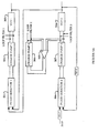
- Figure 2 shows a typical prior art read channel system, which consists of an analog front end, which comprises AGC 201, programmable equalizer filter 202, and data qualifier 204, a time base generator 210 and data synchronizer 206 and 207.
- Full wave rectifier 203 couples the output of equalizer filter 202 to AGC 201 in a feedback loop.
- An output of data qualifier 204 is coupled to PLL1 205 and data synchronizer 206.
- Another output of data qualifier 204 is coupled to PLL2 208 and data synchronizer 207.
- the data qualifier 204 transforms each valid analog read data pulses into a digital pulse, while preserving the relative time position of each valid pulse edge.
- a reference signal FREF is coupled to time base generator 210, which is coupled to PLL3 209.
- the output of time base generator 210 is coupled to PLL1 205, PLL2 208, and CLOCK terminals. Both time base generator 210 and data synchronizers 206 and 207 are based on a PLL circuit.
- Time base generator 210 is programmed to provide a stable reference frequency for data synchronizers.
- the output clock of time base generator 210 can be either PLL3 209 output or time base generator's FREE input signal.
- the read signal is sliced by the floating slice level in the data qualifier.
- the signal comprises both edges of the pit mark.
- the formed pit length depends on the recording conditions (write power, media, slew rate of the laser driver, etc.) and data pattern. Hence, both edges (leading edge and trailing edge) need to be treated independently. As both edges require separate PLLs, and are synchronized independently, the decode window margins may also vary.
- 3 PLL circuits in a read channel circuit There are usually 3 PLL circuits in a read channel circuit: 2 PLL circuits for the data synchronizer, and one PLL for the time base generator.
- the output clock of the time base generator 210 is used as the reference clock for the data synchronizer PLLs in the idle mode and write clock in write mode.
- the 3 PLL circuits in the chip are asynchronous. Also, it is inefficient to include 3 PLL circuits in the same chip since it requires bigger die size and may deteriorate the jitter performance of the clock outputs. Since the PLL circuit is an analog based solution (including VCO and phase detector), the circuit area is large compared to other circuits in the read channel IC.
- the present invention discloses a fully integrated data synchronization circuit for both optical and magneto-optical disk drive (ODD and MOD) read channel system.
- the data synchronization system comprises dual data synchronizers that provide read reference clocks.
- Dual PLL circuits are coupled to the data synchronizers to provide a stable reference frequency to data synchronizers.
- One of the two data synchronizers is used to obtain leading edge data, while the other is for trailing edge data.
- Each PLL circuit comprises a phase detector, a charge pump, and a VCO.
- a loop filter is used in conjunction with a charge pump to control loop characteristics of the PLLs.
- one of the PLLs is used as a time base generator to provide a stable reference frequency to data synchronizers. Once data synchronizers achieve lock using the stable reference frequency and switch over to read data, the time base generator PLL is switched over to function as a data synchronizer PLL in a read mode.
- one of the PLLs is used as both time base generator and data synchronizer PLL, thereby eliminating the need for extra PLL circuitry and requiring only two PLL circuits to support time base generation and data synchronization, reducing die size and power dissipation and improving jitter performance.
- the invention also allows synchronous locking of data synchronizers, minimizing decode window margin variations.
- the servo information permits the definition of individual data tracks on the data surfaces of the disk drive.
- the data tracks may be further divided into a plurality of smaller fields, or "sectors".
- a header field can be used to independently verify the location of individual sectors and tracks.
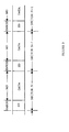
- Figure 3 illustrates a format of data track encoding in a servo sector scheme.
- a header field precedes each data sector on each data track and contains identifier (ID) information which is unique to that sector over the entire drive.
- ID identifier
- a typical identifier includes the track number and the sector number.
- the header may also contain other information related to media defects and redundancy information for error detection.
- the controller reads the header of each data sector as it is encountered and applies various tests to the information contained therein, including the comparison of the ID which was read to the ID which was expected. If the various tests are passed and the ID read matches the ID expected, then the subsequent data part of the sector is read or written appropriately. Because each sector is uniquely and independently identified, the incorrect identification of any sector will not affect the correct identification of any subsequent sectors.
- a sector comprises offset detection field (ODE) and a recording field in which 512, 1024 or 2048 user data bytes can be recorded.
- ODE offset detection field
- a recording field in which 512, 1024 or 2048 user data bytes can be recorded.
- the header of each sector is embossed (pre-formatted).
- the emboss area is also known as pre-pit.
- the length of the header field is defined as 63 bytes.
- the emboss period is 19.3 ⁇ s
- user data periods are 211.2 ⁇ sec/512 byte sector and 766 ,usec/2048 byte sector in outer track; when the emboss period is 34.6 us, user data periods are 369 ⁇ sec/512 byte sector and 1370 ⁇ sec/2048 byte sector in inner track.
- the disk rotation speed is 3000 rpm at 50 Hz.
- the recording field can be empty, user-written or embossed.
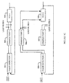
- Figure 4 shows an embodiment of the invention. As can be seen in Figure 4, this embodiment uses two PLL circuits for time base generation and data synchronization.
- an output of data qualifier 404 is coupled to PLL1 405 and data synchronizer 406.
- Another output of data qualifier 404 is coupled to PLL2 408 and data synchronizer/time base generator 407.
- a reference signal FREF is coupled to data synchronizer/time base generator 407.
- PLL2 408 is coupled to PLL1 405 and data synchronizer/time base generator 407.
- the PLL2 408 serves both as a time base generator in idle mode and second data synchronizer PLL in read mode.
- an output of data synchronizer 1 is coupled to SDO1 and an output of data synchronizer 2 is coupled to SDO2, SDO1 represents leading edge data while SDO2 represents trailing edge data.
- An output of PLL1 is coupled to RRC1 and an output of PLL2 is coupled to RRC2.
- Another output of PLL2 408 is coupled to CLOCK.
- block 407 comprises a time base generator and a data synchronizer.
- Data synchronizers 406 and 407 perform data synchronization in the read mode.
- the time base generator portion of 407 provides programmable reference frequency. In idle mode, the time base generator portion of 407 is programmed to provide a stable frequency to the data synchronizer portion of 407. In read mode, however, the phase detector reference is switched from the base generator to the VCO clock signal and the output of the time base generator 407 is only used as a clock count for the sector mark detection window. Switching the source of the phase detector reference from the base generator to the VCO clock signal helps minimize jitter in the data synchronizer PLL.
- the PLL2 408 as a data synchronizer PLL instead of as a time base generator such that it acts as the second synchronizer PLL for the trailing edge of the incoming signal in read mode.
- the time base generator frequency can be maintained via the loop filter voltage.
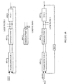
- FIGS 5A, 5B, and 5C show the block diagrams of idle and read operations for PWM mode according to one embodiment of the invention.
- the first PLL loop comprises phase detector 501, charge pump 502, VCO1 503, and loop filter 1.
- Loop filter 1 provides loop voltage to VCO1 503.
- Charge pump 502 increases, decreases, or maintains the loop voltage generated by loop filter 1 to control the VCO frequency.
- Charge pump is well known in the art and is, therefore, not shown in greater detail.
- Loop filters 1, 2, and 3 are external passive filters comprising a capacitor and/or a resistor for controlling PLL locking characteristics.
- the second PLL loop comprising phase detector 506, charge pump 507, VC02 508, loop filter 3 acts as a time base generator PLL with the N+1 and M+1 dividers and provides reference to the FREE input.
- the phase detection rate in an idle mode is dependent on the values of FREF and N+1.
- counters are used to provide divide-by-N and divide-by-M operations.
- the first PLL loop acts as a data synchronizer PLL reference for the time base generator output.
- the voltage of loop filter 2 is maintained to be the same voltage as the loop filter 3 by the comparator 505 having feedback loop through charge pump 504.
- data synchronizers 406 and 407 achieve lock using the output of the time base generator before switching over to read mode.
- PLLs shown in Figure 5A comprises a phase detector, charge pump, and a VCO, it would be appreciated by those skilled in the art that any suitable PLL architecture can be used without departing the scope of the invention.
- the first PLL loop comprising phase detector 501, charge pump 502, VCO 503, and loop filter 1 acts as the first data synchronizer PLL and provides reference to the DRD1*, the leading edge of the data.
- the second PLL loop comprising phase detector 506, charge pump 504, VCO 508 and loop filter 2 acts as a second data synchronizer PLL and provides reference to the DRD2*, the trailing edge of the data.
- loop filter 3 is isolated from the internal circuit. There is no input to the charge pump 3 and loop filter 3 retains the voltage of the idle mode.
- the voltage of loop filter 3 can be maintained by an external capacitor, but would be susceptible to current leakage and may experience voltage drop.
- the maximum period of the MO read mode does not exceed 1370 ⁇ s even at 3000 rpm so that when a 1500 pF capacitor is used in the loop filter 3 and 50 nA leakage current is assumed, the loop filter 3 voltage drop is approximately 46 mV, a negligible amount.
- the VCO control gain is designed to be 0.2 wi rad/VS, less than 1% variation is expected in VCO frequency.
- the VC02 output frequency is dependent on the write drive clock frequency and the disk revolution speed.
- the first and second PLL loops perform the same function as in the MO read mode except that the charge pump 507 is controlled by the outputs of the comparator 505 which has inputs coupled to the outputs of charge pump 507 and charge pump 504. Therefore, the voltage of loop filter 3 is maintained at the same voltage as the loop filter 2 by the comparator 505 having feedback loop through charge pump 3 during this mode.
- This configuration is for the continuous sector read mode.
- the loop filter 3 voltage is maintained at a constant level. However, it is difficult to keep the voltage constant for a long time because of the current leakage.
- the emboss data header
- the loop filter 3 voltage is refreshed with feedback to the charge pump 507 from the comparator 505 output of the voltage difference between loop filter 2 and loop filter 3. Since the header exists in every sector, there is enough time to refresh for at least 19 ⁇ s of the header period. This refresh scheme prevents the voltage of loop filter 3 from drifting due to leakage current.
- the emboss data frequency is independent of the write drive and dependent on the revolution speed of the read drive. In the emboss read mode, the VC02 output frequency is approximately the same as that of the idle mode.
- Loop filters 1, 2, and 3 may use components of different values (for capacitors and/or resistors) to provide different loop filter characteristics depending on the phase detection rates in read and idle modes. It can be seen from Figures 5A, 5B, and 5C that the second PLL loop uses loop filter 3 for time base generation in idle mode and loop filter 2 for phase locking in MO and emboss read modes.
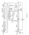
- Figure 5D is a block diagram of an embodiment of the invention.
- DRD1* and the output of VC02 are coupled to switch or multiplexer S1, which selects an input to phase detector 1.
- DRD2* and FREF divided by N+1 are coupled to switch or multiplexer S2, which selects an input to phase detector 2.
- C1 and C2 are control signals for switches or multiplexers S1 and S2, respectively.
- phase detector 2 and comparator 505 are coupled to switch or multiplexer S3, which selects an input to charge pump 2 based upon control signal C3.
- Switch or multiplexer S4 is coupled between phase detector 2 and charge pump 3 to pass the output of phase detector 2 depending upon control signal C4.
- the outputs of charge pumps 2 and 3 are coupled to switch or multiplexer S5, which selects an input to VCO 2 based upon control signal CS.
- M+1 divider has control signal C6 to enable division operation.
- FIGS 6A and 6B show the block diagrams of idle and read operations for PPM (Pit Position Modulation) mode in accordance with one embodiment of the invention.
- VCO 1 and VCO 2 are operated the same way as in the conventional system.
- VCO 2 acts as the time base generator while VCO 1 acts as a data synchronizer VCO.
- Loop filter 2 is not used in this mode.
- Charge pump 2 and loop filter 2 are not used in PPM mode since in PPM, unlike PWM that requires leading edge and trailing edge synchronization, only one synchronization is required.
- phase detector 601 is coupled to charge pump 602, which is coupled to VCO 603.
- An output of VCO 603 is coupled to phase detector 601.
- Phase detector 605 is coupled to charge pump 606, which is coupled to VCO 607.
- An output of VCO 607 is coupled to phase detector 601 and phase detector 605 for feedback.
- phase detector 601 is coupled to charge pump 602, which is coupled to VCO 603.
- An output of VCO 603 is coupled to phase detector 601.
- Input DRD1 is coupled to phase detector 601.
- Phase detector 605 is coupled to charge pump 606, which is coupled to VCO 607.
- An output of VCO 607 is coupled to phase detector 605 in a feedback loop.
- Input FREE is coupled to phase detector 605.
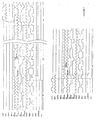
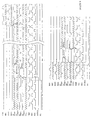
- Figures 7 and 8 show the timing waveforms for the embodiments shown in Figures 5A, 5B, 5C, 6A, and 6B.
- SDO is a synchronized read data output and the leading edge data in PWM mode
- SDO2 is a synchronized read data output and the trailing edge data.
- RRC is a read reference clock output from VCO1 and RRC2 is a read reference clock output from VC02.
- DS1/DRDCK* and DSI/VCOREF2 are phase detector 1 inputs, while DS2/DRDCK* and DS2/VCOREF2 are phase detector 2 inputs.
- FOUT is a time base generator VCO output.
- FREE is the reference frequency for the time base generator.
- RD1 is the row data input signal from the leading edge.
- RD2 is the row data input signal from the trailing edge.
- INTRG2 is the synchronized internal read gate signal and RG is the asynchronous read gate signal.
- Figure 7 shows lock-on/lock-ending sequence waveform diagrams in PPM mode.
- Read gate (RG) signal initiates the PLL locking sequence and selected the PLL reference input.
- the RG is asserted to the high level, the DS1/VCOREF2(VCO1) is reset by the second falling edge of the FOUT.
- the next zero-phase restart is between DS1/DRDCK* and VC01 at the rising edge of the DS1/DRDCK* from the third RD1.
- the internal counter counts the nineteenth RD1
- the RRC and SDO outputs are enabled.
- the RG is negated, the DS1/VCOREF2 (VC01) is reset by the second falling edge of the FOUT, and zero-phase between VC02 and VC01 to restart at the rising edge of second or third DS1/DRDCK* pulse.
- Figure 8 shows lock-on/lock-ending sequence waveform diagrams in PWM mode.
- the DS1/VCOREF2(VC01) and DS2/VCOREF2 are reset by the second falling edge of the FOUT.
- the next zero-phase restart is between DS1 /DRDCK* and VCO at the rising edge of the DS1/DRDCK* from the second RD1.
- Another zero-phase restart is between DS2/DRDCK* and VC02 at the rising edge of the DS2/DRDCK* from the second RD2.
- the VCOs are reset, the input of phase detector 1 in Figure 5 is switched from VC02 output to the DRD1*.
- phase detector 2 The input of phase detector 2 is switched from FREF/(N+1) to DRD2* and charge pump 3 to charge pump 2. DRD1* and DRD2* are delayed read data pulses. As the loop filter 2 voltage and loop filter 3 voltage are maintained by comparator feedback, the VC02 oscillates at the same frequency as in the idle mode. The gain of the comparator is about 6 dB, and the input offset is less than 10 mV.
- the RRC, RRC2, SDO and SD02 outputs are enabled.
- the RG is negated, the DS1/VCOREF2 (VC01) and DS2/VCOREF2 (VC02) are reset by the second falling edge of the FOIST (same as VC02), and zero-phase restart between YC02 and FREF at the rising edge of the second FREF pulse.
- Another zero-phase restart is between VC01 and VC02 at the rising edge of second restarted VC02 pulse.
- the present invention thus provides accurate and reliable time base generator and data synchronizer.
- the advantages of the invention are particularly valuable in dual PLL data synchronization system.
- the advantages of the present invention include:
- the read channel IC requires only two PLLS for PPM and PWM applications, thus saving valuable silicon real estate and cost.
- data synchronizers are synchronized by a common reference signal, minimizing decode window margin variations.
- die size and power dissipation are reduced and jitter performance is improved.
Landscapes
- Engineering & Computer Science (AREA)
- Signal Processing (AREA)
- Stabilization Of Oscillater, Synchronisation, Frequency Synthesizers (AREA)
- Signal Processing For Digital Recording And Reproducing (AREA)
Abstract
Description
Claims (22)
- A data synchronization system comprising:a first data synchronizer;a second data synchronizer;a first phase locked loop (PLL) coupled to said first data synchronizer; anda second PLL coupled to said second data synchronizer.
- The system of Claim 1, wherein said first PLL comprises:a first phase detector;a first charge pump; anda first voltage controlled oscillator (VCO).
- The system of Claim 1 or Claim 2, wherein said second PLL comprises:a phase detector;a second charge pump; anda second voltage controlled oscillator (VCO).
- The system of Claim 3 further comprising:a third charge pump; anda comparator switchably coupled to the second charge pump and to said third charge pump.
- The system of any of Claims 2 to 4, wherein said first PLL further comprises a first loop filter coupled to said first charge pump.
- The system of any of Claims 3 to 5, wherein said second PLL further comprises a second loop filter coupled to said second charge pump.
- The system of any of Claims 4 to 6 further comprising:
a third loop filter coupled to said third charge pump. - The system of any of Claims 3 to 7, wherein said second PLL further comprises;
a frequency divider coupled to said second VCO and said second phase detector in a feedback loop. - The system of any of Claims 3 to 8, further comprising;
a comparator and a second charge pump with an output of said first charge pump and an output of said second charge pump arranged to be coupled to the input terminals of said comparator, said comparator providing an output to said first charge pump in a feedback loop. - The system of any of Claims 3 to 9, further comprising;
a comparator and a second charge pump with an output of said first charge pump and an output of said second charge pump arranged to be coupled to the input terminals of said comparator, said comparator providing an output to said second charge pump in a feedback loop. - A method of data synchronization in a data synchronization system having a first and a second PLL, a first and a second data synchronizer, said first PLL coupled to said first data synchronizer, said second PLL switchably coupled to said second data synchronizer and to said first PLL, the method comprising the steps of:
providing a reference signal to said second PLL; using said second PLL as a time base generator to provide a stable reference frequency to said first and said second data synchronizers. - The method of Claim 11, further comprising providing a first PLL comprising a first phase detector, a first charge pump coupled to said first phase detector, a first loop filter coupled to said first charge pump, and a first VCO coupled to said charge pump, the method comprising the steps of:using said first charge pump to control the output frequency of said VCO; andusing said first loop filter to control the loop characteristics of said first PLL.
- The method of Claim 11 or Claim 12, further comprising providing a second PLL comprising a second phase detector switchably coupled to a second charge pump and a third charge pump, and a second VCO switchably coupled to said second and third charge pumps, the method further comprising the step of:
using said second charge pump to control the output frequency of said second VCO. - The method of Claim 13, further comprising providing a second PLL further comprises a second loop filter coupled to said second charge pump said method further comprising the step of:
using said second loop filter to control the loop characteristics of said second PLL. - The method of Claim 13 or Claim 14 further comprising the step of:
using said third charge pump to control the output frequency of said second VCO. - The method of any of Claims 13 to 15, further comprising providing a second PLL comprising a third loop filter coupled to said third charge pump said method further comprising the step of:
using said third loop filter to control the loop characteristics of said second PLL. - A method of data synchronization in a data synchronization system having a first and a second PLL, a first and a second data synchronizer, said first PLL coupled to said first data synchronizer, said second PLL switchably coupled to said second data synchronizer and to said first PLL, the method comprising the steps of:providing a reference signal to said second PLL in an idle mode;using said second PLL as a time base generator to provide a stable reference frequency to said first and said second data synchronizers in said idle mode;providing a delayed read data signal to said second PLL in a read mode;changing loop characteristics of said second PLL for said read mode.
- The method of Claim 17, further comprising providing a second PLL comprising a phase detector switchably coupled to a first charge pump and a second charge pump, and a VCO switchably coupled to said first and second charge pumps, the method further comprising the steps of:using said first charge pump to control the output frequency of said VCO in said read mode; andusing said second charge pump to control the output frequency of said VCO in said idle mode.
- The method of Claim 18, further comprising providing a second PLL further comprising a comparator switchably coupled to said first and said second charge pumps, the method further comprising the steps of:connecting the outputs of said first charge pump and said second charge pump to said comparator; andconnecting an output of said comparator to said first charge pump in said idle mode.
- The method of Claim 19 further comprising the step of:
connecting an output of said comparator to said second charge pump in said read mode. - The method of any of Claims 18 to 20 further comprising the step of:
connecting the output of said first charge pump to said VCO in said read mode. - The method of any of Claims 18 to 21, further comprising the step of:
connecting the output of said second charge pump to said VCO in said idle mode.
Applications Claiming Priority (2)
| Application Number | Priority Date | Filing Date | Title |
|---|---|---|---|
| US08/691,353 US6067335A (en) | 1996-08-02 | 1996-08-02 | Read channel IC for dual PLL solution |
| US691353 | 2000-10-18 |
Publications (3)
| Publication Number | Publication Date |
|---|---|
| EP0822664A2 true EP0822664A2 (en) | 1998-02-04 |
| EP0822664A3 EP0822664A3 (en) | 1999-08-18 |
| EP0822664B1 EP0822664B1 (en) | 2016-10-12 |
Family
ID=24776212
Family Applications (1)
| Application Number | Title | Priority Date | Filing Date |
|---|---|---|---|
| EP97305794.6A Expired - Lifetime EP0822664B1 (en) | 1996-08-02 | 1997-08-01 | System and method for synchronising data |
Country Status (6)
| Country | Link |
|---|---|
| US (1) | US6067335A (en) |
| EP (1) | EP0822664B1 (en) |
| JP (1) | JPH10293974A (en) |
| KR (1) | KR19980018324A (en) |
| SG (1) | SG65669A1 (en) |
| TW (1) | TW387085B (en) |
Cited By (2)
| Publication number | Priority date | Publication date | Assignee | Title |
|---|---|---|---|---|
| WO2000041307A1 (en) * | 1998-12-16 | 2000-07-13 | International Business Machines Corporation | Combined read and write vco for dasd prml channels |
| EP2075710A2 (en) | 2007-12-31 | 2009-07-01 | STMicroelectronics S.r.l. | Communication system between first and second independently clocked devices |
Families Citing this family (10)
| Publication number | Priority date | Publication date | Assignee | Title |
|---|---|---|---|---|
| JP2000174888A (en) * | 1998-12-09 | 2000-06-23 | Sharp Corp | Communication device |
| US6680970B1 (en) * | 2000-05-23 | 2004-01-20 | Hewlett-Packard Development Company, L.P. | Statistical methods and systems for data rate detection for multi-speed embedded clock serial receivers |
| JP2002290233A (en) * | 2001-03-27 | 2002-10-04 | Fujitsu Ltd | Mode switching method of PLL circuit and mode control circuit of PLL circuit |
| JP2003152694A (en) * | 2001-11-14 | 2003-05-23 | Mitsubishi Electric Corp | Data clock recovery device |
| US7116740B1 (en) | 2003-01-29 | 2006-10-03 | Cisco Technology, Inc. | Method and system for providing clock signals |
| US6970030B1 (en) * | 2003-10-01 | 2005-11-29 | Silicon Laboratories, Inc. | Dual phased-locked loop structure having configurable intermediate frequency and reduced susceptibility to interference |
| US20060001494A1 (en) * | 2004-07-02 | 2006-01-05 | Bruno Garlepp | Cascaded locked-loop circuits deriving high-frequency, low noise clock signals from a jittery, low-frequency reference |
| US7844847B2 (en) * | 2006-09-18 | 2010-11-30 | Samsung Electronics Co., Ltd. | System and method for tuning power consumption and group delay in wireless RFICs |
| KR100834979B1 (en) | 2006-12-20 | 2008-06-03 | 삼성전자주식회사 | A tact switch module performing a toggling operation and a power switching module including the tact switch module. |
| JP5598161B2 (en) * | 2010-08-26 | 2014-10-01 | ヤマハ株式会社 | Clock generation circuit |
Citations (3)
| Publication number | Priority date | Publication date | Assignee | Title |
|---|---|---|---|---|
| US3900890A (en) | 1974-05-06 | 1975-08-19 | Sperry Rand Corp | Speed tolerant recording and recovery system |
| EP0453253A2 (en) | 1990-04-20 | 1991-10-23 | International Business Machines Corporation | Timing signal generator for signal processing system |
| JPH0490168A (en) | 1990-08-02 | 1992-03-24 | Fujitsu Ltd | Data reproducing circuit for magneto-optical disk device |
Family Cites Families (16)
| Publication number | Priority date | Publication date | Assignee | Title |
|---|---|---|---|---|
| US3701039A (en) * | 1968-10-28 | 1972-10-24 | Ibm | Random binary data signal frequency and phase compensation circuit |
| FR2194091B1 (en) * | 1972-05-10 | 1977-04-01 | Centre Nat Etd Spatiales | |
| KR900001593B1 (en) * | 1985-03-30 | 1990-03-15 | 가부시끼가이샤 도오시바 | Digital signal reproducing circuit |
| US4953185A (en) * | 1988-10-05 | 1990-08-28 | Motorola Inc. | Clock recovery and hold circuit for digital TDM mobile radio |
| US5206885A (en) * | 1989-02-06 | 1993-04-27 | Motorola, Inc. | Selective call receiver with fast bit synchronizer |
| US5128809A (en) * | 1989-06-29 | 1992-07-07 | Digital Equipment Corporation | Coherent multi-frequency synthesis |
| JPH0332132A (en) * | 1989-06-29 | 1991-02-12 | Canon Inc | Digital signal decoder |
| US5170297A (en) * | 1990-07-13 | 1992-12-08 | Standard Microsystems Corporation | Current averaging data separator |
| US5206889A (en) * | 1992-01-17 | 1993-04-27 | Hewlett-Packard Company | Timing interpolator |
| JPH06259890A (en) * | 1993-03-03 | 1994-09-16 | Fuji Electric Co Ltd | Reproducing device for magnetic recording data |
| JPH0730533A (en) * | 1993-07-12 | 1995-01-31 | Sony Corp | Sync detection circuit |
| JP3133885B2 (en) * | 1993-12-24 | 2001-02-13 | 富士通株式会社 | Signal processing device having PLL circuit |
| US5834980A (en) * | 1994-01-03 | 1998-11-10 | Lucent Technologies Inc. | Method and apparatus for supplying synchronization signals securing as clock signals with defined phase relationships |
| US5450458A (en) * | 1994-08-05 | 1995-09-12 | International Business Machines Corporation | Method and apparatus for phase-aligned multiple frequency synthesizer with synchronization window decoder |
| US5414390A (en) * | 1994-09-12 | 1995-05-09 | Analog Devices, Inc. | Center frequency controlled phase locked loop system |
| US5528638A (en) * | 1995-05-24 | 1996-06-18 | Sun Microsystems, Inc. | Multiple phase shifted clocks generation using a minimal set of signals from a PLL |
-
1996
- 1996-08-02 US US08/691,353 patent/US6067335A/en not_active Expired - Lifetime
-
1997
- 1997-08-01 EP EP97305794.6A patent/EP0822664B1/en not_active Expired - Lifetime
- 1997-08-02 SG SG1997002772A patent/SG65669A1/en unknown
- 1997-08-02 KR KR1019970037092A patent/KR19980018324A/en not_active Ceased
- 1997-08-04 JP JP9241673A patent/JPH10293974A/en active Pending
- 1997-10-01 TW TW086111090A patent/TW387085B/en not_active IP Right Cessation
Patent Citations (3)
| Publication number | Priority date | Publication date | Assignee | Title |
|---|---|---|---|---|
| US3900890A (en) | 1974-05-06 | 1975-08-19 | Sperry Rand Corp | Speed tolerant recording and recovery system |
| EP0453253A2 (en) | 1990-04-20 | 1991-10-23 | International Business Machines Corporation | Timing signal generator for signal processing system |
| JPH0490168A (en) | 1990-08-02 | 1992-03-24 | Fujitsu Ltd | Data reproducing circuit for magneto-optical disk device |
Cited By (3)
| Publication number | Priority date | Publication date | Assignee | Title |
|---|---|---|---|---|
| WO2000041307A1 (en) * | 1998-12-16 | 2000-07-13 | International Business Machines Corporation | Combined read and write vco for dasd prml channels |
| US6313962B1 (en) | 1998-12-16 | 2001-11-06 | International Business Machines Corporation | Combined read and write VCO for DASD PRML channels |
| EP2075710A2 (en) | 2007-12-31 | 2009-07-01 | STMicroelectronics S.r.l. | Communication system between first and second independently clocked devices |
Also Published As
| Publication number | Publication date |
|---|---|
| JPH10293974A (en) | 1998-11-04 |
| EP0822664B1 (en) | 2016-10-12 |
| EP0822664A3 (en) | 1999-08-18 |
| TW387085B (en) | 2000-04-11 |
| KR19980018324A (en) | 1998-06-05 |
| US6067335A (en) | 2000-05-23 |
| SG65669A1 (en) | 1999-06-22 |
Similar Documents
| Publication | Publication Date | Title |
|---|---|---|
| US7126776B1 (en) | Disk drive having a sector clock that is synchronized to the angular speed of the spindle motor | |
| US4633488A (en) | Phase-locked loop for MFM data recording | |
| US5388090A (en) | Method, apparatus, and medium for recording information in data sections having number of bytes which increases with increase in circumference of tracks on medium | |
| US5414689A (en) | Optical information recording/reproducing apparatus using pit edge recording system | |
| US5535067A (en) | Frequency controlled reference clock generator | |
| US4688205A (en) | Data demodulation apparatus | |
| US6067335A (en) | Read channel IC for dual PLL solution | |
| EP0763825B1 (en) | Data detection apparatus | |
| US6181655B1 (en) | Optical disc drive, timing signal generator, and information recording and reproduction method | |
| US6873483B2 (en) | Disk drive with servo synchronous recording | |
| US5623477A (en) | Optical recording disk capable of resynchronization in digital encoding and decoding | |
| US7016284B2 (en) | Method and related circuit for generating a wobble clock and an ATIP clock through a reference clock and a wobble signal | |
| EP0674314A1 (en) | A data recording medium, an optical disk and an optical disk apparatus | |
| US5864531A (en) | DC level fluctuation correction by selecting a time constant coupled to a reproduced signal | |
| US6961293B2 (en) | Method and related device for achieving stable writing state of compact disk drive by adjusting writing clock | |
| US6690631B2 (en) | Clock generation circuit and integrated circuit for reproducing an audio signal comprising such a clock generation circuit | |
| JPH05314664A (en) | Information recording medium, information recording / reproducing method, and information recording / reproducing apparatus | |
| US6313962B1 (en) | Combined read and write VCO for DASD PRML channels | |
| KR100217185B1 (en) | Controlling device of input voltage of vco of pll for reproducing multi-type disk | |
| USRE39832E1 (en) | Optical recording disk capable of resynchronization in digital encoding and decoding | |
| JPH0757384A (en) | Disk player | |
| JPH08263845A (en) | Optical information recording / reproducing device | |
| JPH0729299A (en) | Disk device | |
| JPS63298870A (en) | Signal reproducing system |
Legal Events
| Date | Code | Title | Description |
|---|---|---|---|
| PUAI | Public reference made under article 153(3) epc to a published international application that has entered the european phase |
Free format text: ORIGINAL CODE: 0009012 |
|
| AK | Designated contracting states |
Kind code of ref document: A2 Designated state(s): DE FR GB IT NL |
|
| PUAL | Search report despatched |
Free format text: ORIGINAL CODE: 0009013 |
|
| AK | Designated contracting states |
Kind code of ref document: A3 Designated state(s): AT BE CH DE DK ES FI FR GB GR IE IT LI LU MC NL PT SE |
|
| 17P | Request for examination filed |
Effective date: 20000218 |
|
| AKX | Designation fees paid |
Free format text: DE FR GB IT NL |
|
| GRAP | Despatch of communication of intention to grant a patent |
Free format text: ORIGINAL CODE: EPIDOSNIGR1 |
|
| INTG | Intention to grant announced |
Effective date: 20160426 |
|
| GRAS | Grant fee paid |
Free format text: ORIGINAL CODE: EPIDOSNIGR3 |
|
| GRAA | (expected) grant |
Free format text: ORIGINAL CODE: 0009210 |
|
| AK | Designated contracting states |
Kind code of ref document: B1 Designated state(s): DE FR GB IT NL |
|
| REG | Reference to a national code |
Ref country code: GB Ref legal event code: FG4D |
|
| REG | Reference to a national code |
Ref country code: DE Ref legal event code: R096 Ref document number: 69740866 Country of ref document: DE |
|
| REG | Reference to a national code |
Ref country code: NL Ref legal event code: MP Effective date: 20161012 |
|
| PG25 | Lapsed in a contracting state [announced via postgrant information from national office to epo] |
Ref country code: NL Free format text: LAPSE BECAUSE OF FAILURE TO SUBMIT A TRANSLATION OF THE DESCRIPTION OR TO PAY THE FEE WITHIN THE PRESCRIBED TIME-LIMIT Effective date: 20161012 |
|
| REG | Reference to a national code |
Ref country code: DE Ref legal event code: R097 Ref document number: 69740866 Country of ref document: DE |
|
| REG | Reference to a national code |
Ref country code: DE Ref legal event code: R071 Ref document number: 69740866 Country of ref document: DE |
|
| PLBE | No opposition filed within time limit |
Free format text: ORIGINAL CODE: 0009261 |
|
| STAA | Information on the status of an ep patent application or granted ep patent |
Free format text: STATUS: NO OPPOSITION FILED WITHIN TIME LIMIT |
|
| 26N | No opposition filed |
Effective date: 20170713 |
|
| REG | Reference to a national code |
Ref country code: GB Ref legal event code: PE20 Expiry date: 20170731 |
|
| PG25 | Lapsed in a contracting state [announced via postgrant information from national office to epo] |
Ref country code: GB Free format text: LAPSE BECAUSE OF EXPIRATION OF PROTECTION Effective date: 20170731 |