EP0817362B1 - Multiple output, zero voltage switching, series resonant VHF inverter - Google Patents
Multiple output, zero voltage switching, series resonant VHF inverter Download PDFInfo
- Publication number
- EP0817362B1 EP0817362B1 EP97110393A EP97110393A EP0817362B1 EP 0817362 B1 EP0817362 B1 EP 0817362B1 EP 97110393 A EP97110393 A EP 97110393A EP 97110393 A EP97110393 A EP 97110393A EP 0817362 B1 EP0817362 B1 EP 0817362B1
- Authority
- EP
- European Patent Office
- Prior art keywords
- resonant
- capacitor
- inductor
- network
- circuit
- Prior art date
- Legal status (The legal status is an assumption and is not a legal conclusion. Google has not performed a legal analysis and makes no representation as to the accuracy of the status listed.)
- Expired - Lifetime
Links
- 239000003990 capacitor Substances 0.000 claims description 104
- 230000000737 periodic effect Effects 0.000 claims description 16
- 238000010586 diagram Methods 0.000 description 4
- 230000001105 regulatory effect Effects 0.000 description 4
- 238000006243 chemical reaction Methods 0.000 description 1
- 230000000694 effects Effects 0.000 description 1
Images
Classifications
-
- H—ELECTRICITY
- H02—GENERATION; CONVERSION OR DISTRIBUTION OF ELECTRIC POWER
- H02M—APPARATUS FOR CONVERSION BETWEEN AC AND AC, BETWEEN AC AND DC, OR BETWEEN DC AND DC, AND FOR USE WITH MAINS OR SIMILAR POWER SUPPLY SYSTEMS; CONVERSION OF DC OR AC INPUT POWER INTO SURGE OUTPUT POWER; CONTROL OR REGULATION THEREOF
- H02M7/00—Conversion of AC power input into DC power output; Conversion of DC power input into AC power output
- H02M7/42—Conversion of DC power input into AC power output without possibility of reversal
- H02M7/44—Conversion of DC power input into AC power output without possibility of reversal by static converters
- H02M7/48—Conversion of DC power input into AC power output without possibility of reversal by static converters using discharge tubes with control electrode or semiconductor devices with control electrode
- H02M7/53—Conversion of DC power input into AC power output without possibility of reversal by static converters using discharge tubes with control electrode or semiconductor devices with control electrode using devices of a triode or transistor type requiring continuous application of a control signal
- H02M7/537—Conversion of DC power input into AC power output without possibility of reversal by static converters using discharge tubes with control electrode or semiconductor devices with control electrode using devices of a triode or transistor type requiring continuous application of a control signal using semiconductor devices only, e.g. single switched pulse inverters
-
- H—ELECTRICITY
- H02—GENERATION; CONVERSION OR DISTRIBUTION OF ELECTRIC POWER
- H02M—APPARATUS FOR CONVERSION BETWEEN AC AND AC, BETWEEN AC AND DC, OR BETWEEN DC AND DC, AND FOR USE WITH MAINS OR SIMILAR POWER SUPPLY SYSTEMS; CONVERSION OF DC OR AC INPUT POWER INTO SURGE OUTPUT POWER; CONTROL OR REGULATION THEREOF
- H02M1/00—Details of apparatus for conversion
- H02M1/0083—Converters characterised by their input or output configuration
- H02M1/009—Converters characterised by their input or output configuration having two or more independently controlled outputs
-
- Y—GENERAL TAGGING OF NEW TECHNOLOGICAL DEVELOPMENTS; GENERAL TAGGING OF CROSS-SECTIONAL TECHNOLOGIES SPANNING OVER SEVERAL SECTIONS OF THE IPC; TECHNICAL SUBJECTS COVERED BY FORMER USPC CROSS-REFERENCE ART COLLECTIONS [XRACs] AND DIGESTS
- Y02—TECHNOLOGIES OR APPLICATIONS FOR MITIGATION OR ADAPTATION AGAINST CLIMATE CHANGE
- Y02B—CLIMATE CHANGE MITIGATION TECHNOLOGIES RELATED TO BUILDINGS, e.g. HOUSING, HOUSE APPLIANCES OR RELATED END-USER APPLICATIONS
- Y02B70/00—Technologies for an efficient end-user side electric power management and consumption
- Y02B70/10—Technologies improving the efficiency by using switched-mode power supplies [SMPS], i.e. efficient power electronics conversion e.g. power factor correction or reduction of losses in power supplies or efficient standby modes
Definitions
- DC to AC inverters are commonly employed in applications which require the conversion of DC power to AC power, including for example power supplies.
- DC to AC inverters have been designed to operate in the VHF range of frequencies since higher frequencies allow for significantly smaller passive components and also provide for faster feedback response to load perturbations.
- multiple power supply outputs are required, for example a main output and one or more auxiliary output.
- this is accomplished by the use of separate inverters, or power splitters for dividing the output of a single inverter.
- said switching means includes a transistor having a first terminal and a second terminal, and an inductor connected between said first terminal and the supply voltage
- said first resonant circuit includes a first resonant circuit first capacitor connected between said first terminal and said second terminal, and a first resonant circuit inductor and a first resonant circuit second capacitor serially connected between said first terminal and said first load circuit
- said second resonant circuit includes a second resonant circuit first capacitor which is connected between said first terminal and said second terminal and which can be combined with said first resonant circuit first capacitor, and a second resonant circuit inductor and a second resonant circuit second capacitor serially connected between said first terminal and said second load circuit.
- the above object is achieved by the second DC to AC inverter, mentioned at the outset, wherein said first resonant waveshaping network being comprised of a first capacitor and a first inductor connected in series between a first supply voltage node and a first central node, said first supply voltage node being at a positive voltage relative to ground, said second resonant waveshaping network being comprised of a second capacitor and a second inductor connected in series between said first supply voltage node and a second central node, said first switching means being connected across said first capacitor and said second capacitor, said first switching means being driven with a first periodic drive signal of a predetermined frequency, a third resonant waveshaping network comprised of a third capacitor and a third inductor connected in series between a second supply voltage node and the first central node, said second supply voltage node being at a voltage that is less than said positive voltage, a fourth resonant waveshaping network comprised of a fourth capacitor and a fourth inductor connected in series between the first
- FIG. 1 set forth therein is a schematic diagram of a VHF DC to AC inverter in accordance H with the invention which includes an RF choke 11 having one terminal connected to a supply node 101 which is connected to a supply voltage V IN that is positive relative to a ground reference.
- the other terminal of the RF choke 11 is connected to the collector terminal of an NPN transistor 13.
- the emitter terminal of the NPN transistor 13 is connected to a ground reference potential, while the base of the NPN transistor 13 is driven with a periodic drive voltage signal DR which has a predetermined frequency F 0 .
- the periodic drive voltage signal DR comprises a sinusoid. .
- a capacitor C11 is connected between the collector of the NPN transistor 13 and the ground, and an inductor L11 is connected between the collector of the NPN transistor 13 and one terminal of a capacitor C12.
- the other terminal of the capacitor C12 is connected to a load circuit 33 which can be a regulated load.
- the VHF DC to AC inverter of FIG. 1 further includes a capacitor C21 that is connected between the collector of the NPN transistor 13 and the ground, and an inductor L21 that is connected between the collector of the NPN transistor 13 and one terminal of a capacitor C22.
- the other terminal of the capacitor C22 is connected to a load circuit 43 which can be a regulated load.
- the capacitor C11, the inductor L11, and the capacitor C12 form a first resonant waveshaping network, while the capacitor C21, the inductor L21, and the capacitor C22 form a second resonant waveshaping network.
- These networks are tuned to substantially the same frequency, for example in the range of about .8F 0 to about .9F 0 , where F 0 is the frequency of the periodic drive signal DR, but are configured to deliver different amounts of power.
- the ratios of the values of corresponding elements in the first and second resonant waveshaping networks are determined by the ratio of the power provided to the load circuits 33, 43.
- the ratio between the value of the capacitor C11 of the first waveshaping network and the value of the capacitor C21 of the second waveshaping network is A/B (i.e., the value of C21 is B/A tines the value of C11).
- the ratio between the value of the inductor L11 of the first waveshaping network and the value of the inductor L21 of the second waveshaping network is B/A (i.e., the value of L21 is A/B times the value of L11).
- the ratio between the value of the capacitor C12 of the first waveshaping network and the value of the capacitor C22 of the second resonant waveshaping network is A/B (i.e., the value of C22 is B/A times the value of C12).
- the switch 13 (which can alternatively be implemented as a power FET), the capacitor C11, the inductor L11, and the capacitor C12, together with the RF choke 11 comprise a conventional class E VHF DC-AC inverter, configured to deliver a power A to the load circuit 33.
- the capacitor C21, the inductor L21, and the capacitor C22 also comprise a resonant waveshaping network that functions similarly to the resonant network comprised of the capacitor C11, the inductor L11, and the capacitor C12, and together with the switch 13 and the RF choke 11 comprise a conventional class E VHF DC-AC inverter, configured to deliver a power B to the load circuit 43.
- the switch 13 and the RF choke 11 perform functions for both resonant circuits, and the capacitor C11 can be combined with the capacitor C21.
- two inverters are realized with one switch 13, one RF choke 11, and one collector-emitter capacitor (or drain-source capacitor if the switch 13 is implemented with an FET).
- a separate AC output is provided by only one additional inductor and one additional capacitor.
- the power splitter approach referred to in the background discussion would require two additional inductors, two additional capacitors, and an additional resistor.
- FIG. 2 set forth therein is a schematic diagram of a series resonant half bridge VHF DC to AC inverter in accordance with the invention which includes a capacitor C111 having one terminal connected to a first supply node 201 which is connected to a supply voltage V IN that is positive relative to a ground reference.
- the other terminal of the capacitor C111 is connected to one terminal of an inductor L111 which has its other terminal connected to a first central node 103.
- the collector terminal of a first NPN transistor 115 is connected to the first supply node 201, while the emitter of the first NPN transistor 115 is connected to the node between the capacitor C111 and the inductor L111.
- the base of the first NPN transistor 115 is driven with a first periodic drive voltage signal DR1 which has a predetermined frequency.
- a capacitor C221 has one terminal connected to the first supply node 201 which is connected to the supply voltage V IN that is positive relative to a ground reference.
- the other terminal of the capacitor C221 is connected to one terminal of an inductor L221 which has its other terminal connected to second central node 203.
- the first NPN transistor 115 comprises an active switch that provides an open circuit when it is open or non-conductive, and electrically connects the terminals of the capacitors C111, C221 when it is conductive.
- the capacitor C111 and the inductor L111 comprise a first resonant waveshaping network, while the capacitor C221 and the inductor L221 comprise a second resonant waveshaping network.
- the DC to AC inverter of FIG. 2 further comprises a capacitor C331 having one terminal connected to a second supply node 202 which is connected to a second supply voltage -V IN that is negative with respect to the first supply voltage V IN .
- the other terminal of the capacitor C331 is connected to one terminal of an inductor L331 which has its other terminal connected to the first central node 103.
- the collector terminal of a second NPN transistor 125 is connected to the node between the capacitor C331 and the inductor L331, while the emitter of the second NPN transistor 125 is connected to the second supply node 202.
- the base of the second NPN transistor 125 is driven with a second periodic drive voltage signal DR2 which is of the same predetermined frequency as the first periodic drive voltage signal DR1, but is 180 degrees out of phase with respect to the first periodic drive voltage signal DR1.
- a capacitor C441 has one terminal connected to the second supply node 202 which is connected to the second supply voltage -V IN that is negative with respect to the first supply voltage V IN .
- the other terminal of the capacitor C441 is connected to one terminal of an inductor L441 which has its other terminal connected to the second central node 203.
- the second NPN transistor 125 comprises an active switch that provides an open circuit when it is open or non-conductive, and electrically connects the two terminals of the capacitors C331, C441 when it is conductive.
- the capacitor C331 and the inductor L331 comprise a third resonant waveshaping network, while the capacitor C441 and the inductor L441 comprise a fourth resonant waveshaping network.
- a first LC bandpass filter 130 connected to the first central node 103 is responsive to the first and third resonant waveshaping networks formed of the capacitors C111, C331 and the inductors L111, L331, and provides power to a first load circuit 133 which can be a regulated load.
- a second LC bandpass filter 140 connected to the second central node 103 is responsive to the second and fourth resonant waveshaping networks formed of the capacitors C221, C441 and the inductors L221, L441, and provides power to a second load circuit 143 which can be a regulated load.
- the first resonant network formed by elements C111, L111 and the third resonant network formed by the elements C331, L331 are substantially identical.
- the second resonant network formed by elements C221, L221 and the fourth resonant network formed by the elements C441, L441 are substantially identical. These networks are tuned to substantially the same frequency, but are configured to deliver different amounts of power.
- the ratios of the values of corresponding elements in the first resonant waveshaping network (C111, L111) and the second resonant waveshaping network (C221, L221) are determined by the ratio of the power provided to the load circuits 133, 143.
- the ratios of the values of corresponding elements in the third resonant waveshaping network (C331, L331) and the fourth resonant waveshaping network (C331, L441) are determined by the ratio of the power provided to the load circuits 133, 143.
- the ratio of the power delivered to the first load circuit 133 and the power delivered to the second load circuit 143 is A/B
- the ratio between the value of the capacitor C111 of the first waveshaping network and the value of the capacitor C221 of the second waveshaping network is A/B (i.e., the value of C221 is B/A times the value of C111).
- the ratio between the value of the inductor L111 of the first waveshaping network and the value of the inductor L221 of the second waveshaping network is B/A (i.e., the value of L221 is A/B times the value of L111).
- the ratio between the value of the capacitor C331 of the third waveshaping network and the value of the capacitor C441 of the fourth waveshaping network is A/B (i.e., the value of C441 is B/A times the value of C331).
- the ratio between the value of the inductor L331 of the third waveshaping network and the value of the inductor L441 of the fourth waveshaping network is B/A (i.e., the value of L441 is A/B times the value of L331).
- the capacitance of C111 is substantially equal to the capacitance of C331, and the inductance of L111 is substantially equal to the inductance of L331.
- the second resonant network (C221, L221) and the fourth resonant network (C441, L441) are substantially identical, and the capacitance of C221 is substantially equal to the capacitance of C441, while the inductance of L221 is substantially equal to the inductance of L441.
- the inductors L111, L221, L331, L441 prevent rapid buildup of current, which allows the transistors 115, 125 to be advantageously driven with a 50 percent duty cycle.
- the first and second periodic drive voltage signals DR1, DR2 can comprise sinusoids which are easily produced in the VHF range.
- the frequency of the periodic drive voltage signals DR1, DR2 is in the range of 30 MHz to 200 MHz.
- the resonant waveshaping networks can be tuned for example to a resonant frequency that is in the range of 0.75F 0 to 1.1F 0 , wherein F 0 is the frequency of the periodic drive voltage signals DR1, DR2 and thus the operating frequency of the inverter of FIG. 2.
- the switches 115, 125, the capacitors C111, C331, the inductors L111, L331, and the bandpass filter 130 more particularly comprise a series-resonant half-bridge VHF DC-AC inverter configured to supply a power A to the load circuit 133.
- the capacitor C111 and the inductor L111 comprise a resonant network which ensures that the voltage Vce across the switch 115 is zero when the switch 115 is turned on, and that the voltage Vce across the switch 115 will rise slowly from zero when the switch 115 is turned off, thus allowing the switch current to drop to zero before appreciable switch voltage has built up.
- the capacitor C331 and the inductor L331 perform a similar function for the switch 125.
- the switch 115 is on when the switch 125 is off, and the switch 125 is on when the switch 115 is off.
- the switches 115, 125, the capacitors C221, C441, the inductors L221, L441, and the bandpass filter 140 comprise a series-resonant half-bridge VHF DC-AC inverter configured to supply a power B to the load circuit 143.
- This inverter behaves in substantially the same manner as the inverter comprised of the switches 115, 125, the capacitors C111, C331, the inductors L111, L331, and the bandpass filter 130, described above.
- the capacitor C221 performs the same function as the capacitor C111
- the inductor L221 performs the same function as the inductor L111.
- the capacitor C441 performs the same function as the capacitor C331, and the inductor L441 performs the same function as the inductor L331.
- the bandpass filter 140 performs the same function as the bandpass filter 130.
- VHF DC to AC inverters that efficiently provide for multiple outputs with reduced complexity, comprising switching circuitry and multiple resonant waveshaping networks connected between the switching circuitry and respective load circuits.
Landscapes
- Engineering & Computer Science (AREA)
- Power Engineering (AREA)
- Inverter Devices (AREA)
- Supply And Distribution Of Alternating Current (AREA)
Description
- DC to AC inverters are commonly employed in applications which require the conversion of DC power to AC power, including for example power supplies. DC to AC inverters have been designed to operate in the VHF range of frequencies since higher frequencies allow for significantly smaller passive components and also provide for faster feedback response to load perturbations.
- In many applications multiple power supply outputs are required, for example a main output and one or more auxiliary output. Typically, this is accomplished by the use of separate inverters, or power splitters for dividing the output of a single inverter.
- Considerations with separate inverters and power splitters include complexity, reduced efficiency, and increased parts count. A further consideration with power splitters is the effect of regulation of one power splitter port on another power splitter port.
- It would therefore be an advantage to provide an improved VHF DC to AC inverter that provides multiple outputs.
- This object is achieved by the VHF DC to AC inverter, mentioned at the outset, wherein said switching means includes a transistor having a first terminal and a second terminal, and an inductor connected between said first terminal and the supply voltage, said first resonant circuit includes a first resonant circuit first capacitor connected between said first terminal and said second terminal, and a first resonant circuit inductor and a first resonant circuit second capacitor serially connected between said first terminal and said first load circuit, and said second resonant circuit includes a second resonant circuit first capacitor which is connected between said first terminal and said second terminal and which can be combined with said first resonant circuit first capacitor, and a second resonant circuit inductor and a second resonant circuit second capacitor serially connected between said first terminal and said second load circuit.
- Further, the above object is achieved by the second DC to AC inverter, mentioned at the outset, wherein
said first resonant waveshaping network being comprised of a first capacitor and a first inductor connected in series between a first supply voltage node and a first central node, said first supply voltage node being at a positive voltage relative to ground,
said second resonant waveshaping network being comprised of a second capacitor and a second inductor connected in series between said first supply voltage node and a second central node,
said first switching means being connected across said first capacitor and said second capacitor, said first switching means being driven with a first periodic drive signal of a predetermined frequency,
a third resonant waveshaping network comprised of a third capacitor and a third inductor connected in series between a second supply voltage node and the first central node, said second supply voltage node being at a voltage that is less than said positive voltage,
a fourth resonant waveshaping network comprised of a fourth capacitor and a fourth inductor connected in series between the second supply voltage node and the second central node,
said second switching means being connected across said third and fourth capacitors, said second switching means being driven with a second periodic signal of said predetermined frequency and being out of phase by 180 degrees relative to said first periodic drive signal,
a first bandpass filter connected to said first central node and responsive to said first resonant waveshaping network and said third resonant waveshaping network,
said first load circuit being responsive to said first bandpass filter,
a second bandpass filter connected to said second central node and responsive to said second resonant waveshaping network and said fourth resonant waveshaping network, and
said second load circuit being responsive to said second bandpass filter. - The advantages and features of the disclosed invention will readily be appreciated by persons skilled in the art from the following detailed description when read in conjunction with the drawing wherein:
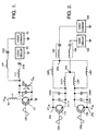
- FIG. 1 is a schematic circuit diagram of a multiple output class E VHF DC to AC inverter in accordance with the invention.
- FIG. 2 is a schematic diagram of a multiple output series resonant half bridge VHF DC to AC inverter in accordance with the invention.
-
- In the following detailed description and in the several figures of the drawing, like elements are identified with like reference numerals.
Referring now to FIG. 1, set forth therein is a schematic diagram of a VHF DC to AC inverter in accordance H with the invention which includes anRF choke 11 having one terminal connected to asupply node 101 which is connected to a supply voltage VIN that is positive relative to a ground reference. The other terminal of theRF choke 11 is connected to the collector terminal of anNPN transistor 13. The emitter terminal of theNPN transistor 13 is connected to a ground reference potential, while the base of theNPN transistor 13 is driven with a periodic drive voltage signal DR which has a predetermined frequency F0. By way of illustrative example, the periodic drive voltage signal DR comprises a sinusoid. . - A capacitor C11 is connected between the collector of the
NPN transistor 13 and the ground, and an inductor L11 is connected between the collector of theNPN transistor 13 and one terminal of a capacitor C12. The other terminal of the capacitor C12 is connected to aload circuit 33 which can be a regulated load. - The VHF DC to AC inverter of FIG. 1 further includes a capacitor C21 that is connected between the collector of the
NPN transistor 13 and the ground, and an inductor L21 that is connected between the collector of theNPN transistor 13 and one terminal of a capacitor C22. The other terminal of the capacitor C22 is connected to aload circuit 43 which can be a regulated load. - The capacitor C11, the inductor L11, and the capacitor C12 form a first resonant waveshaping network, while the capacitor C21, the inductor L21, and the capacitor C22 form a second resonant waveshaping network. These networks are tuned to substantially the same frequency, for example in the range of about .8F0 to about .9F0, where F0 is the frequency of the periodic drive signal DR, but are configured to deliver different amounts of power. Thus, the ratios of the values of corresponding elements in the first and second resonant waveshaping networks are determined by the ratio of the power provided to the
load circuits - The switch 13 (which can alternatively be implemented as a power FET), the capacitor C11, the inductor L11, and the capacitor C12, together with the
RF choke 11 comprise a conventional class E VHF DC-AC inverter, configured to deliver a power A to theload circuit 33. The capacitor C11, the inductor L11, and the capacitor C12 comprise a resonant waveshaping network that ensures that the voltage Vce across theswitch 13 is zero when theswitch 13 is turned on, and that the voltage Vce across theswitch 13 will rise slowly (from Vce = Vsat ≈ 0) when the switch is turned off, thus allowing switch current to drop to zero before appreciable switch voltage has built up. - The capacitor C21, the inductor L21, and the capacitor C22 also comprise a resonant waveshaping network that functions similarly to the resonant network comprised of the capacitor C11, the inductor L11, and the capacitor C12, and together with the
switch 13 and theRF choke 11 comprise a conventional class E VHF DC-AC inverter, configured to deliver a power B to theload circuit 43. - When the two inverter circuits in the inverter of FIG. 1 are operated together, elements in parallel can be combined. Thus, the
switch 13 and theRF choke 11 perform functions for both resonant circuits, and the capacitor C11 can be combined with the capacitor C21. Effectively, two inverters are realized with oneswitch 13, oneRF choke 11, and one collector-emitter capacitor (or drain-source capacitor if theswitch 13 is implemented with an FET). Thus, a separate AC output is provided by only one additional inductor and one additional capacitor. In contrast, the power splitter approach referred to in the background discussion would require two additional inductors, two additional capacitors, and an additional resistor. - Referring now to FIG. 2, set forth therein is a schematic diagram of a series resonant half bridge VHF DC to AC inverter in accordance with the invention which includes a capacitor C111 having one terminal connected to a
first supply node 201 which is connected to a supply voltage VIN that is positive relative to a ground reference. The other terminal of the capacitor C111 is connected to one terminal of an inductor L111 which has its other terminal connected to a firstcentral node 103. The collector terminal of afirst NPN transistor 115 is connected to thefirst supply node 201, while the emitter of thefirst NPN transistor 115 is connected to the node between the capacitor C111 and the inductor L111. The base of thefirst NPN transistor 115 is driven with a first periodic drive voltage signal DR1 which has a predetermined frequency. - A capacitor C221 has one terminal connected to the
first supply node 201 which is connected to the supply voltage VIN that is positive relative to a ground reference. The other terminal of the capacitor C221 is connected to one terminal of an inductor L221 which has its other terminal connected to secondcentral node 203. - The
first NPN transistor 115 comprises an active switch that provides an open circuit when it is open or non-conductive, and electrically connects the terminals of the capacitors C111, C221 when it is conductive. The capacitor C111 and the inductor L111 comprise a first resonant waveshaping network, while the capacitor C221 and the inductor L221 comprise a second resonant waveshaping network. - The DC to AC inverter of FIG. 2 further comprises a capacitor C331 having one terminal connected to a
second supply node 202 which is connected to a second supply voltage -VIN that is negative with respect to the first supply voltage VIN. The other terminal of the capacitor C331 is connected to one terminal of an inductor L331 which has its other terminal connected to the firstcentral node 103. The collector terminal of asecond NPN transistor 125 is connected to the node between the capacitor C331 and the inductor L331, while the emitter of thesecond NPN transistor 125 is connected to thesecond supply node 202. The base of thesecond NPN transistor 125 is driven with a second periodic drive voltage signal DR2 which is of the same predetermined frequency as the first periodic drive voltage signal DR1, but is 180 degrees out of phase with respect to the first periodic drive voltage signal DR1. - A capacitor C441 has one terminal connected to the
second supply node 202 which is connected to the second supply voltage -VIN that is negative with respect to the first supply voltage VIN. The other terminal of the capacitor C441 is connected to one terminal of an inductor L441 which has its other terminal connected to the secondcentral node 203. - The
second NPN transistor 125 comprises an active switch that provides an open circuit when it is open or non-conductive, and electrically connects the two terminals of the capacitors C331, C441 when it is conductive. The capacitor C331 and the inductor L331 comprise a third resonant waveshaping network, while the capacitor C441 and the inductor L441 comprise a fourth resonant waveshaping network. - A first
LC bandpass filter 130 connected to the firstcentral node 103 is responsive to the first and third resonant waveshaping networks formed of the capacitors C111, C331 and the inductors L111, L331, and provides power to afirst load circuit 133 which can be a regulated load. A secondLC bandpass filter 140 connected to the secondcentral node 103 is responsive to the second and fourth resonant waveshaping networks formed of the capacitors C221, C441 and the inductors L221, L441, and provides power to asecond load circuit 143 which can be a regulated load. - The first resonant network formed by elements C111, L111 and the third resonant network formed by the elements C331, L331 are substantially identical. Similarly, the second resonant network formed by elements C221, L221 and the fourth resonant network formed by the elements C441, L441 are substantially identical. These networks are tuned to substantially the same frequency, but are configured to deliver different amounts of power. Thus, the ratios of the values of corresponding elements in the first resonant waveshaping network (C111, L111) and the second resonant waveshaping network (C221, L221) are determined by the ratio of the power provided to the
load circuits load circuits first load circuit 133 and the power delivered to thesecond load circuit 143 is A/B, the ratio between the value of the capacitor C111 of the first waveshaping network and the value of the capacitor C221 of the second waveshaping network is A/B (i.e., the value of C221 is B/A times the value of C111). Correspondingly, the ratio between the value of the inductor L111 of the first waveshaping network and the value of the inductor L221 of the second waveshaping network is B/A (i.e., the value of L221 is A/B times the value of L111). The ratio between the value of the capacitor C331 of the third waveshaping network and the value of the capacitor C441 of the fourth waveshaping network is A/B (i.e., the value of C441 is B/A times the value of C331). Correspondingly, the ratio between the value of the inductor L331 of the third waveshaping network and the value of the inductor L441 of the fourth waveshaping network is B/A (i.e., the value of L441 is A/B times the value of L331). - Insofar as the first resonant network (C111, L111) and the third resonant network (C331, L331) are substantially identical, the capacitance of C111 is substantially equal to the capacitance of C331, and the inductance of L111 is substantially equal to the inductance of L331. Similarly, the second resonant network (C221, L221) and the fourth resonant network (C441, L441) are substantially identical, and the capacitance of C221 is substantially equal to the capacitance of C441, while the inductance of L221 is substantially equal to the inductance of L441.
- More particularly as to the drive signals DR1, DR2, the inductors L111, L221, L331, L441 prevent rapid buildup of current, which allows the
transistors transistors - The
switches bandpass filter 130 more particularly comprise a series-resonant half-bridge VHF DC-AC inverter configured to supply a power A to theload circuit 133. The capacitor C111 and the inductor L111 comprise a resonant network which ensures that the voltage Vce across theswitch 115 is zero when theswitch 115 is turned on, and that the voltage Vce across theswitch 115 will rise slowly from zero when theswitch 115 is turned off, thus allowing the switch current to drop to zero before appreciable switch voltage has built up. The capacitor C331 and the inductor L331 perform a similar function for theswitch 125. - In operation, since the drive signals DR1, DR2 are 180 degrees out of phase, the
switch 115 is on when theswitch 125 is off, and theswitch 125 is on when theswitch 115 is off. - When the
switch 115 is on, current is delivered from the node 201 (which is connected to VIN) through the inductor L111 into thenode 103. Some of the current is delivered into the bandpass filter 130 (where harmonic content is filtered) and hence into theload circuit 133. The rest of the current provides energy for the resonant circuit comprised of the capacitor C331 and the inductor L331. Similarly, when theswitch 125 is on, current is returned from theload circuit 133 through thebandpass filter 130 into thenode 103. Some the current returns through the inductor L331 into thenode 202 which is connected to -VIN. The rest of the current provides energy for the resonant circuit formed by the capacitor C111 and the inductor L111. - The
switches bandpass filter 140 comprise a series-resonant half-bridge VHF DC-AC inverter configured to supply a power B to theload circuit 143. This inverter behaves in substantially the same manner as the inverter comprised of theswitches bandpass filter 130, described above. Thus, the capacitor C221 performs the same function as the capacitor C111, and the inductor L221 performs the same function as the inductor L111. The capacitor C441 performs the same function as the capacitor C331, and the inductor L441 performs the same function as the inductor L331. Thebandpass filter 140 performs the same function as thebandpass filter 130. - When the two inverter circuits of the inverter of FIG. 2 are operated together, elements in parallel can be combined. Thus, the
switches - The foregoing has thus been a disclosure of VHF DC to AC inverters that efficiently provide for multiple outputs with reduced complexity, comprising switching circuitry and multiple resonant waveshaping networks connected between the switching circuitry and respective load circuits.
- Although the foregoing has been a description and illustration of specific embodiments of the invention these should not be construed as limiting the scope of the invention as defined by the appended claims.
Claims (10)
- A VHF DC to AC inverter comprising:characterized in that:switching means (13) connected between a supply voltage (VIN) and a reference voltage;a first resonant waveshaping network (C11, L11, C12) responsive to said switching means (13);a first load circuit (33) responsive to said first resonant waveshaping network (C11, L11, C12);a second resonant waveshaping network (C21, L21, C22) responsive to said switching means (13); anda second load circuit (43) responsive to said second resonant waveshaping network (C21, L21, C22),said switching means (13) includes a transistor (13) having a first terminal and a second terminal, and an inductor (11) connected between said first terminal and the supply voltage (VIN);said first resonant circuit (C11, L11, C12) includes a first resonant circuit first capacitor (C11) connected between said first terminal and said second terminal, and a first resonant circuit inductor (L11) and a first resonant circuit second capacitor (C12) serially connected between said first terminal and said first load circuit (33); andsaid second resonant circuit (C21, L21, C22) includes a second resonant circuit first capacitor (C21) which is connected between said first terminal and said second terminal and which can be combined with said first resonant circuit first capacitor (C11), and a second resonant circuit inductor (L21) and a second resonant circuit second capacitor (C22) serially connected between said first terminal and said second load circuit (43).
- The inverter of claim 1, characterized in that the values of said first resonant circuit first capacitor (C11), inductor (L11), and second capacitor (C12) are respectively proportional relative to the values of said second resonant circuit first capacitor (C21), inductor (L12) and second capacitor (C22) in accordance with a ratio of power delivered to said first load circuit (33) and power delivered to said second load circuit (43).
- The inverter of claim 2, characterized in that:the ratio of power delivered to said first load circuit (33) and power delivered to said second load circuit (43) is A/B;the ratio between the value of said first resonant circuit first capacitor (C11) and the value of said second resonant circuit first capacitor (C21) is A/B;the ratio between the value of said first resonant circuit inductor (L11) and the value of said second resonant circuit inductor (L21) is B/A; andthe ratio between the value of said first resonant circuit second capacitor (C12) and the value of said second resonant circuit second capacitor (C22) is A/B.
- A DC to AC inverter comprising a first resonant waveshaping network (C111, L111), a second resonant waveshaping network (C221, L221), first switching means (115), second switching means (125), a first load circuit (133) and a second load circuit,
characterized by
said first resonant waveshaping network (C111, L111) being comprised of a first capacitor (C111) and a first inductor (L111) connected in series between a first supply voltage node (201) and a first central node (103), said first supply voltage node (201) being at a positive voltage (VIN) relative to ground;
said second resonant waveshaping network (C221, L221) being comprised of a second capacitor (C221) and a second inductor (L221) connected in series between the first supply voltage node (201) and a second central node (203);
said first switching means (115) being connected across said first capacitor (C111) and said second capacitor (C221), said first switching means (115) being driven with a first periodic drive signal (DR1) of a predetermined frequency (F0);
a third resonant waveshaping network (C331, L331) comprised of a third capacitor (C331) and a third inductor (L331) connected in series between a second supply voltage node (202) and the first central node (103), said second supply voltage node (202) being at a voltage (-VIN) that is less than said positive voltage (VIN);
a fourth resonant waveshaping network (C441, L441) comprised of a fourth capacitor (C441) and a fourth inductor (L441) connected in series between the second supply voltage node (202) and the second central node (203);
said second switching means (125) being connected across said third and fourth capacitors (C331, C441), said second switching means (125) being driven with a second periodic signal (DR2) of said predetermined frequency (F0) and being out of phase by 180 degrees relative to said first periodic drive signal (DR1);
a first bandpass filter (130) connected to said first central node (103) and responsive to said first resonant waveshaping network (C111, L111) and said third resonant waveshaping network (C331, L331);
said first load circuit (133) being responsive to said first bandpass filter (130);
a second bandpass filter (140) connected to said second central node (203) and responsive to said second resonant waveshaping network (C221, L221) and said fourth resonant waveshaping network (C441, L441); and
said second load circuit (143) being responsive to said second bandpass filter (140). - The inverter of claim 4, characterized in that said first resonant waveshaping network (C111, L111) and said third resonant waveshaping network (C331, L331) are substantially identical.
- The inverter of claim 5, characterized in that the values of said first resonant network capacitor (C111) and inductor (L111) are respectively proportional relative to the values of said second resonant circuit capacitor (C221) and inductor (L221) in accordance with a ratio of power delivered to said first load circuit (133) and power delivered to said second load circuit (143), and wherein the values of said third resonant network capacitor (C331) and inductor (L331) are respectively proportional relative to the values of said fourth resonant circuit capacitor (C441) and inductor (L441) in accordance with the ratio of power delivered to said first load circuit (133) and power delivered to said second load circuit (143).
- The inverter of claim 6, characterized in that:the ratio of power delivered to said first load circuit (133) and power delivered to said second load circuit (143) is A/B;the ratio between the value of said first resonant network capacitor (C111) and the value of said second resonant network capacitor (C221) is A/B;the ratio between the value of said first resonant network inductor (L111) and the value of said second resonant network inductor (L221) is B/A;the ratio between the value of said third resonant network capacitor (C331) and the value of said fourth resonant network capacitor (C441) is A/B;the ratio between the value of said third resonant network inductor (L331) and the value of said fourth resonant network inductor (L441) is B/A.
- The inverter to any of claims 4 - 6, characterized in that said second supply voltage node (202) is at ground.
- The inverter of any of claims 4 - 6, characterized in that said second supply voltage node (202) is at a negative voltage (-VIN) relative to ground.
- The inverter of any of claims 4 - 8, characterized in that said first switching means (115) comprises a first NPN transistor (115), and said second switching means (125) comprises a second NPN transistor (125).
Applications Claiming Priority (2)
| Application Number | Priority Date | Filing Date | Title |
|---|---|---|---|
| US671035 | 1996-06-27 | ||
| US08/671,035 US5668715A (en) | 1996-06-27 | 1996-06-27 | Multiple output, zero voltage switching, series resonant VHF inverter |
Publications (3)
| Publication Number | Publication Date |
|---|---|
| EP0817362A2 EP0817362A2 (en) | 1998-01-07 |
| EP0817362A3 EP0817362A3 (en) | 1998-12-23 |
| EP0817362B1 true EP0817362B1 (en) | 2003-10-29 |
Family
ID=24692885
Family Applications (1)
| Application Number | Title | Priority Date | Filing Date |
|---|---|---|---|
| EP97110393A Expired - Lifetime EP0817362B1 (en) | 1996-06-27 | 1997-06-25 | Multiple output, zero voltage switching, series resonant VHF inverter |
Country Status (7)
| Country | Link |
|---|---|
| US (1) | US5668715A (en) |
| EP (1) | EP0817362B1 (en) |
| JP (1) | JP3037640B2 (en) |
| AU (1) | AU690491B2 (en) |
| CA (1) | CA2208646C (en) |
| DE (1) | DE69725788T2 (en) |
| ES (1) | ES2205090T3 (en) |
Families Citing this family (5)
| Publication number | Priority date | Publication date | Assignee | Title |
|---|---|---|---|---|
| GB9806415D0 (en) * | 1998-03-26 | 1998-05-20 | Raytec Components Limited | Dx1 power regulator |
| EP1987468B1 (en) * | 2006-02-15 | 2018-05-23 | Tyco Fire & Security GmbH | Rf switched rfid multiplexer |
| CN102195510B (en) * | 2010-03-08 | 2014-09-03 | 苏州奥曦特电子科技有限公司 | Single-switch oscillating inverter |
| JP5846426B2 (en) * | 2011-11-30 | 2016-01-20 | 国立大学法人神戸大学 | High frequency inverter for induction heating and its control method |
| GB2607063B (en) * | 2021-05-27 | 2023-09-06 | Dyson Technology Ltd | Power inverter |
Family Cites Families (7)
| Publication number | Priority date | Publication date | Assignee | Title |
|---|---|---|---|---|
| US3878481A (en) * | 1973-11-02 | 1975-04-15 | Westinghouse Electric Corp | Low noise VHF oscillator with circuit matching transistors |
| DE3112499A1 (en) * | 1981-03-30 | 1982-10-14 | Patra Patent Treuhand | Ballast arrangement for operating low-pressure discharge lamps |
| JPS5959047U (en) * | 1982-10-13 | 1984-04-17 | アルプス電気株式会社 | UHF-VHF combination tuner |
| JPS61113437U (en) * | 1984-12-26 | 1986-07-17 | ||
| US5162963A (en) * | 1989-03-14 | 1992-11-10 | Hughes Aircraft Company | Surge eliminator for switching converters |
| JP2828881B2 (en) * | 1993-10-04 | 1998-11-25 | 沖電気工業株式会社 | High voltage power circuit |
| US5410276A (en) * | 1993-12-28 | 1995-04-25 | Hughes Aircraft Company | RF modulation using a pulsed DC power supply |
-
1996
- 1996-06-27 US US08/671,035 patent/US5668715A/en not_active Expired - Lifetime
-
1997
- 1997-06-24 CA CA002208646A patent/CA2208646C/en not_active Expired - Fee Related
- 1997-06-25 ES ES97110393T patent/ES2205090T3/en not_active Expired - Lifetime
- 1997-06-25 EP EP97110393A patent/EP0817362B1/en not_active Expired - Lifetime
- 1997-06-25 DE DE69725788T patent/DE69725788T2/en not_active Expired - Lifetime
- 1997-06-26 AU AU28341/97A patent/AU690491B2/en not_active Ceased
- 1997-06-27 JP JP9172333A patent/JP3037640B2/en not_active Expired - Fee Related
Also Published As
| Publication number | Publication date |
|---|---|
| DE69725788T2 (en) | 2004-05-13 |
| CA2208646C (en) | 2000-02-29 |
| EP0817362A3 (en) | 1998-12-23 |
| AU690491B2 (en) | 1998-04-23 |
| DE69725788D1 (en) | 2003-12-04 |
| CA2208646A1 (en) | 1997-12-27 |
| JPH10117483A (en) | 1998-05-06 |
| US5668715A (en) | 1997-09-16 |
| ES2205090T3 (en) | 2004-05-01 |
| EP0817362A2 (en) | 1998-01-07 |
| JP3037640B2 (en) | 2000-04-24 |
| AU2834197A (en) | 1998-01-22 |
Similar Documents
| Publication | Publication Date | Title |
|---|---|---|
| EP0798846B1 (en) | Zero voltage switching, series resonant half bridge VHF inverter | |
| US5332951A (en) | Circuit for driving gas discharge lamps having protection against diode operation of the lamps | |
| US6008589A (en) | Single-switch, high power factor, ac-to-ac power converters | |
| US5708573A (en) | Varactor controlled fixed frequency VHF DC-DC converter | |
| KR20040004398A (en) | Class e/f switching power amplifiers | |
| US5677601A (en) | Operating circuit for low-power low-pressure discharge lamps, particularly compact fluorescent lamps | |
| JPH0693602B2 (en) | Switching circuit arrangement for a tuner that switches between two frequency bands | |
| Kazimierczuk et al. | Class-E amplifier with an inductive impedance inverter | |
| US5495404A (en) | Multi-resonant inverter | |
| US5668715A (en) | Multiple output, zero voltage switching, series resonant VHF inverter | |
| KR970703643A (en) | Variable Frequency Oscillator Circuit (VARIABLE-FREQUENCY OSCILLATOR CIRCUIT) | |
| CA2149327A1 (en) | Circuit arrangement for operating low-pressure discharge lamps | |
| JPH0191672A (en) | Inverter device | |
| US20020075414A1 (en) | Television tuner having less distortion | |
| KR930003235B1 (en) | N-Phase Sine Wave Converter | |
| US5703771A (en) | VHF inverter with self regulation for any load | |
| SU1658328A1 (en) | Dc voltage converter | |
| JPS576574A (en) | Transistor inverter device | |
| CN100546163C (en) | Circuit arrangement for inductive transfer of electrical energy | |
| JPH0422573Y2 (en) | ||
| Matsuo et al. | Resonant DC/DC converter using Class DE oscillator | |
| SU1480067A1 (en) | Single-clock inverter with sine output voltage | |
| JPS627774B2 (en) | ||
| JPH06351241A (en) | High voltage power supply circuit | |
| JPH06351242A (en) | High voltage power supply circuit |
Legal Events
| Date | Code | Title | Description |
|---|---|---|---|
| PUAI | Public reference made under article 153(3) epc to a published international application that has entered the european phase |
Free format text: ORIGINAL CODE: 0009012 |
|
| AK | Designated contracting states |
Kind code of ref document: A2 Designated state(s): DE ES GB IT |
|
| RAP1 | Party data changed (applicant data changed or rights of an application transferred) |
Owner name: RAYTHEON COMPANY |
|
| PUAL | Search report despatched |
Free format text: ORIGINAL CODE: 0009013 |
|
| RAP1 | Party data changed (applicant data changed or rights of an application transferred) |
Owner name: RAYTHEON COMPANY |
|
| AK | Designated contracting states |
Kind code of ref document: A3 Designated state(s): AT BE CH DE DK ES FI FR GB GR IE IT LI LU MC NL PT SE |
|
| 17P | Request for examination filed |
Effective date: 19990526 |
|
| AKX | Designation fees paid |
Free format text: DE ES GB IT |
|
| GRAH | Despatch of communication of intention to grant a patent |
Free format text: ORIGINAL CODE: EPIDOS IGRA |
|
| GRAS | Grant fee paid |
Free format text: ORIGINAL CODE: EPIDOSNIGR3 |
|
| GRAA | (expected) grant |
Free format text: ORIGINAL CODE: 0009210 |
|
| AK | Designated contracting states |
Kind code of ref document: B1 Designated state(s): DE ES GB IT |
|
| REG | Reference to a national code |
Ref country code: GB Ref legal event code: FG4D |
|
| REF | Corresponds to: |
Ref document number: 69725788 Country of ref document: DE Date of ref document: 20031204 Kind code of ref document: P |
|
| REG | Reference to a national code |
Ref country code: ES Ref legal event code: FG2A Ref document number: 2205090 Country of ref document: ES Kind code of ref document: T3 |
|
| PLBE | No opposition filed within time limit |
Free format text: ORIGINAL CODE: 0009261 |
|
| STAA | Information on the status of an ep patent application or granted ep patent |
Free format text: STATUS: NO OPPOSITION FILED WITHIN TIME LIMIT |
|
| 26N | No opposition filed |
Effective date: 20040730 |
|
| PGFP | Annual fee paid to national office [announced via postgrant information from national office to epo] |
Ref country code: IT Payment date: 20120619 Year of fee payment: 16 |
|
| PGFP | Annual fee paid to national office [announced via postgrant information from national office to epo] |
Ref country code: ES Payment date: 20120726 Year of fee payment: 16 |
|
| REG | Reference to a national code |
Ref country code: GB Ref legal event code: 732E Free format text: REGISTERED BETWEEN 20130228 AND 20130306 |
|
| REG | Reference to a national code |
Ref country code: DE Ref legal event code: R082 Ref document number: 69725788 Country of ref document: DE Representative=s name: BOSCH JEHLE PATENTANWALTSGESELLSCHAFT MBH, DE |
|
| REG | Reference to a national code |
Ref country code: DE Ref legal event code: R082 Ref document number: 69725788 Country of ref document: DE Representative=s name: BOSCH JEHLE PATENTANWALTSGESELLSCHAFT MBH, DE Effective date: 20130603 Ref country code: DE Ref legal event code: R081 Ref document number: 69725788 Country of ref document: DE Owner name: OL SECURITY LLC, DOVER, US Free format text: FORMER OWNER: RAYTHEON CO., LEXINGTON, MASS., US Effective date: 20130603 Ref country code: DE Ref legal event code: R081 Ref document number: 69725788 Country of ref document: DE Owner name: OL SECURITY LLC, US Free format text: FORMER OWNER: RAYTHEON CO., LEXINGTON, US Effective date: 20130603 |
|
| PG25 | Lapsed in a contracting state [announced via postgrant information from national office to epo] |
Ref country code: IT Free format text: LAPSE BECAUSE OF NON-PAYMENT OF DUE FEES Effective date: 20130625 |
|
| REG | Reference to a national code |
Ref country code: ES Ref legal event code: FD2A Effective date: 20140707 |
|
| PG25 | Lapsed in a contracting state [announced via postgrant information from national office to epo] |
Ref country code: ES Free format text: LAPSE BECAUSE OF NON-PAYMENT OF DUE FEES Effective date: 20130626 |
|
| PGFP | Annual fee paid to national office [announced via postgrant information from national office to epo] |
Ref country code: GB Payment date: 20150526 Year of fee payment: 19 |
|
| PGFP | Annual fee paid to national office [announced via postgrant information from national office to epo] |
Ref country code: DE Payment date: 20150630 Year of fee payment: 19 |
|
| REG | Reference to a national code |
Ref country code: DE Ref legal event code: R119 Ref document number: 69725788 Country of ref document: DE |
|
| GBPC | Gb: european patent ceased through non-payment of renewal fee |
Effective date: 20160625 |
|
| PG25 | Lapsed in a contracting state [announced via postgrant information from national office to epo] |
Ref country code: DE Free format text: LAPSE BECAUSE OF NON-PAYMENT OF DUE FEES Effective date: 20170103 |
|
| PG25 | Lapsed in a contracting state [announced via postgrant information from national office to epo] |
Ref country code: GB Free format text: LAPSE BECAUSE OF NON-PAYMENT OF DUE FEES Effective date: 20160625 |