EP0816896B1 - Optical component - Google Patents
Optical component Download PDFInfo
- Publication number
- EP0816896B1 EP0816896B1 EP97401380A EP97401380A EP0816896B1 EP 0816896 B1 EP0816896 B1 EP 0816896B1 EP 97401380 A EP97401380 A EP 97401380A EP 97401380 A EP97401380 A EP 97401380A EP 0816896 B1 EP0816896 B1 EP 0816896B1
- Authority
- EP
- European Patent Office
- Prior art keywords
- modulator
- metallization
- optical
- polarization
- light guide
- Prior art date
- Legal status (The legal status is an assumption and is not a legal conclusion. Google has not performed a legal analysis and makes no representation as to the accuracy of the status listed.)
- Expired - Lifetime
Links
Images


Classifications
-
- G—PHYSICS
- G02—OPTICS
- G02B—OPTICAL ELEMENTS, SYSTEMS OR APPARATUS
- G02B6/00—Light guides; Structural details of arrangements comprising light guides and other optical elements, e.g. couplings
- G02B6/10—Light guides; Structural details of arrangements comprising light guides and other optical elements, e.g. couplings of the optical waveguide type
- G02B6/12—Light guides; Structural details of arrangements comprising light guides and other optical elements, e.g. couplings of the optical waveguide type of the integrated circuit kind
- G02B6/122—Basic optical elements, e.g. light-guiding paths
- G02B6/125—Bends, branchings or intersections
-
- G—PHYSICS
- G02—OPTICS
- G02F—OPTICAL DEVICES OR ARRANGEMENTS FOR THE CONTROL OF LIGHT BY MODIFICATION OF THE OPTICAL PROPERTIES OF THE MEDIA OF THE ELEMENTS INVOLVED THEREIN; NON-LINEAR OPTICS; FREQUENCY-CHANGING OF LIGHT; OPTICAL LOGIC ELEMENTS; OPTICAL ANALOGUE/DIGITAL CONVERTERS
- G02F1/00—Devices or arrangements for the control of the intensity, colour, phase, polarisation or direction of light arriving from an independent light source, e.g. switching, gating or modulating; Non-linear optics
- G02F1/01—Devices or arrangements for the control of the intensity, colour, phase, polarisation or direction of light arriving from an independent light source, e.g. switching, gating or modulating; Non-linear optics for the control of the intensity, phase, polarisation or colour
- G02F1/03—Devices or arrangements for the control of the intensity, colour, phase, polarisation or direction of light arriving from an independent light source, e.g. switching, gating or modulating; Non-linear optics for the control of the intensity, phase, polarisation or colour based on ceramics or electro-optical crystals, e.g. exhibiting Pockels effect or Kerr effect
- G02F1/035—Devices or arrangements for the control of the intensity, colour, phase, polarisation or direction of light arriving from an independent light source, e.g. switching, gating or modulating; Non-linear optics for the control of the intensity, phase, polarisation or colour based on ceramics or electro-optical crystals, e.g. exhibiting Pockels effect or Kerr effect in an optical waveguide structure
- G02F1/0353—Devices or arrangements for the control of the intensity, colour, phase, polarisation or direction of light arriving from an independent light source, e.g. switching, gating or modulating; Non-linear optics for the control of the intensity, phase, polarisation or colour based on ceramics or electro-optical crystals, e.g. exhibiting Pockels effect or Kerr effect in an optical waveguide structure involving an electro-optic TE-TM mode conversion
-
- G—PHYSICS
- G02—OPTICS
- G02F—OPTICAL DEVICES OR ARRANGEMENTS FOR THE CONTROL OF LIGHT BY MODIFICATION OF THE OPTICAL PROPERTIES OF THE MEDIA OF THE ELEMENTS INVOLVED THEREIN; NON-LINEAR OPTICS; FREQUENCY-CHANGING OF LIGHT; OPTICAL LOGIC ELEMENTS; OPTICAL ANALOGUE/DIGITAL CONVERTERS
- G02F1/00—Devices or arrangements for the control of the intensity, colour, phase, polarisation or direction of light arriving from an independent light source, e.g. switching, gating or modulating; Non-linear optics
- G02F1/01—Devices or arrangements for the control of the intensity, colour, phase, polarisation or direction of light arriving from an independent light source, e.g. switching, gating or modulating; Non-linear optics for the control of the intensity, phase, polarisation or colour
- G02F1/061—Devices or arrangements for the control of the intensity, colour, phase, polarisation or direction of light arriving from an independent light source, e.g. switching, gating or modulating; Non-linear optics for the control of the intensity, phase, polarisation or colour based on electro-optical organic material
- G02F1/065—Devices or arrangements for the control of the intensity, colour, phase, polarisation or direction of light arriving from an independent light source, e.g. switching, gating or modulating; Non-linear optics for the control of the intensity, phase, polarisation or colour based on electro-optical organic material in an optical waveguide structure
-
- G—PHYSICS
- G02—OPTICS
- G02F—OPTICAL DEVICES OR ARRANGEMENTS FOR THE CONTROL OF LIGHT BY MODIFICATION OF THE OPTICAL PROPERTIES OF THE MEDIA OF THE ELEMENTS INVOLVED THEREIN; NON-LINEAR OPTICS; FREQUENCY-CHANGING OF LIGHT; OPTICAL LOGIC ELEMENTS; OPTICAL ANALOGUE/DIGITAL CONVERTERS
- G02F1/00—Devices or arrangements for the control of the intensity, colour, phase, polarisation or direction of light arriving from an independent light source, e.g. switching, gating or modulating; Non-linear optics
- G02F1/01—Devices or arrangements for the control of the intensity, colour, phase, polarisation or direction of light arriving from an independent light source, e.g. switching, gating or modulating; Non-linear optics for the control of the intensity, phase, polarisation or colour
- G02F1/03—Devices or arrangements for the control of the intensity, colour, phase, polarisation or direction of light arriving from an independent light source, e.g. switching, gating or modulating; Non-linear optics for the control of the intensity, phase, polarisation or colour based on ceramics or electro-optical crystals, e.g. exhibiting Pockels effect or Kerr effect
- G02F1/035—Devices or arrangements for the control of the intensity, colour, phase, polarisation or direction of light arriving from an independent light source, e.g. switching, gating or modulating; Non-linear optics for the control of the intensity, phase, polarisation or colour based on ceramics or electro-optical crystals, e.g. exhibiting Pockels effect or Kerr effect in an optical waveguide structure
- G02F1/0356—Devices or arrangements for the control of the intensity, colour, phase, polarisation or direction of light arriving from an independent light source, e.g. switching, gating or modulating; Non-linear optics for the control of the intensity, phase, polarisation or colour based on ceramics or electro-optical crystals, e.g. exhibiting Pockels effect or Kerr effect in an optical waveguide structure controlled by a high-frequency electromagnetic wave component in an electric waveguide structure
-
- G—PHYSICS
- G02—OPTICS
- G02F—OPTICAL DEVICES OR ARRANGEMENTS FOR THE CONTROL OF LIGHT BY MODIFICATION OF THE OPTICAL PROPERTIES OF THE MEDIA OF THE ELEMENTS INVOLVED THEREIN; NON-LINEAR OPTICS; FREQUENCY-CHANGING OF LIGHT; OPTICAL LOGIC ELEMENTS; OPTICAL ANALOGUE/DIGITAL CONVERTERS
- G02F1/00—Devices or arrangements for the control of the intensity, colour, phase, polarisation or direction of light arriving from an independent light source, e.g. switching, gating or modulating; Non-linear optics
- G02F1/01—Devices or arrangements for the control of the intensity, colour, phase, polarisation or direction of light arriving from an independent light source, e.g. switching, gating or modulating; Non-linear optics for the control of the intensity, phase, polarisation or colour
- G02F1/21—Devices or arrangements for the control of the intensity, colour, phase, polarisation or direction of light arriving from an independent light source, e.g. switching, gating or modulating; Non-linear optics for the control of the intensity, phase, polarisation or colour by interference
- G02F1/212—Mach-Zehnder type
-
- G—PHYSICS
- G02—OPTICS
- G02F—OPTICAL DEVICES OR ARRANGEMENTS FOR THE CONTROL OF LIGHT BY MODIFICATION OF THE OPTICAL PROPERTIES OF THE MEDIA OF THE ELEMENTS INVOLVED THEREIN; NON-LINEAR OPTICS; FREQUENCY-CHANGING OF LIGHT; OPTICAL LOGIC ELEMENTS; OPTICAL ANALOGUE/DIGITAL CONVERTERS
- G02F1/00—Devices or arrangements for the control of the intensity, colour, phase, polarisation or direction of light arriving from an independent light source, e.g. switching, gating or modulating; Non-linear optics
- G02F1/01—Devices or arrangements for the control of the intensity, colour, phase, polarisation or direction of light arriving from an independent light source, e.g. switching, gating or modulating; Non-linear optics for the control of the intensity, phase, polarisation or colour
- G02F1/21—Devices or arrangements for the control of the intensity, colour, phase, polarisation or direction of light arriving from an independent light source, e.g. switching, gating or modulating; Non-linear optics for the control of the intensity, phase, polarisation or colour by interference
- G02F1/225—Devices or arrangements for the control of the intensity, colour, phase, polarisation or direction of light arriving from an independent light source, e.g. switching, gating or modulating; Non-linear optics for the control of the intensity, phase, polarisation or colour by interference in an optical waveguide structure
-
- G—PHYSICS
- G02—OPTICS
- G02F—OPTICAL DEVICES OR ARRANGEMENTS FOR THE CONTROL OF LIGHT BY MODIFICATION OF THE OPTICAL PROPERTIES OF THE MEDIA OF THE ELEMENTS INVOLVED THEREIN; NON-LINEAR OPTICS; FREQUENCY-CHANGING OF LIGHT; OPTICAL LOGIC ELEMENTS; OPTICAL ANALOGUE/DIGITAL CONVERTERS
- G02F1/00—Devices or arrangements for the control of the intensity, colour, phase, polarisation or direction of light arriving from an independent light source, e.g. switching, gating or modulating; Non-linear optics
- G02F1/29—Devices or arrangements for the control of the intensity, colour, phase, polarisation or direction of light arriving from an independent light source, e.g. switching, gating or modulating; Non-linear optics for the control of the position or the direction of light beams, i.e. deflection
- G02F1/31—Digital deflection, i.e. optical switching
- G02F1/313—Digital deflection, i.e. optical switching in an optical waveguide structure
- G02F1/3132—Digital deflection, i.e. optical switching in an optical waveguide structure of directional coupler type
-
- G—PHYSICS
- G02—OPTICS
- G02F—OPTICAL DEVICES OR ARRANGEMENTS FOR THE CONTROL OF LIGHT BY MODIFICATION OF THE OPTICAL PROPERTIES OF THE MEDIA OF THE ELEMENTS INVOLVED THEREIN; NON-LINEAR OPTICS; FREQUENCY-CHANGING OF LIGHT; OPTICAL LOGIC ELEMENTS; OPTICAL ANALOGUE/DIGITAL CONVERTERS
- G02F1/00—Devices or arrangements for the control of the intensity, colour, phase, polarisation or direction of light arriving from an independent light source, e.g. switching, gating or modulating; Non-linear optics
- G02F1/29—Devices or arrangements for the control of the intensity, colour, phase, polarisation or direction of light arriving from an independent light source, e.g. switching, gating or modulating; Non-linear optics for the control of the position or the direction of light beams, i.e. deflection
- G02F1/31—Digital deflection, i.e. optical switching
- G02F1/313—Digital deflection, i.e. optical switching in an optical waveguide structure
- G02F1/3136—Digital deflection, i.e. optical switching in an optical waveguide structure of interferometric switch type
-
- G—PHYSICS
- G02—OPTICS
- G02F—OPTICAL DEVICES OR ARRANGEMENTS FOR THE CONTROL OF LIGHT BY MODIFICATION OF THE OPTICAL PROPERTIES OF THE MEDIA OF THE ELEMENTS INVOLVED THEREIN; NON-LINEAR OPTICS; FREQUENCY-CHANGING OF LIGHT; OPTICAL LOGIC ELEMENTS; OPTICAL ANALOGUE/DIGITAL CONVERTERS
- G02F2203/00—Function characteristic
- G02F2203/06—Polarisation independent
Definitions
- the present invention relates to components electro.
- Electrooptical polymers have a strong telecommunications potential. We plans to use them in distribution networks optical to the subscriber (fiber to the home: FTTH, according to Anglo-Saxon terminology generally used by the skilled person) because they are likely to allow manufacture of components at low cost. They allow to simply make waveguides on substrates varied. When the oriented polymer is placed between electrodes, applying an electric field of modulation between the electrodes modulates the index of refraction of the polymer via the Pockels effect. This is translated by a phase shift of the guided optical wave; this phase shift can be used to process the optical signal (modulation, switching, etc.).
- An object of the invention is to propose improvements to known electrooptical components at this day.
- Electrooptical effect there are three types of electrode geometry: geometries planar electrodes, those with transverse electrodes and those with coplanar electrodes.
- optical guides of the components electrooptics known to date are generally almost straight.
- the electrooptical components are indeed usually made from ferroelectric crystals or semiconductors.
- the waveguide is generally achieved by local disturbance of the index of refraction.
- the differences in index between the heart and the sheath of the guides being weak (0.001), the guides optics of these components must have substantially linear geometries to minimize loss of curvature (angle less than 0.1 °).
- the invention provides a component comprising an optical guide whose core is in one electro-optical material, as well as at least one metallization to the right of a portion of said guide, for the control thereof, characterized in that the guide optical is folded and in that the metallization extends at least two portions of the light guide which extend folded over each other.
- the electrooptical material is advantageously a polymer material.
- such a structure finds advantageously applied in the case of components capacitive, i.e. controlled at frequencies lower or around the GHz, since it allows reduce the size or control voltage. We then have a compromise control voltage-bandwidth-size to optimize.
- Metallization is then used as a transmission line microwave and the optical signal propagates in guide portions to the right of which the metallization extends in the same direction and the same direction as the microwave signal that propagates in this metallization.
- Such a component indeed has a length of the reduced microwave line, which limits attenuation of the microwave wave, and reduces the component size.
- the optical guide of the component advantageously comprises a polarization converter disposed between two portions to the right of which extends the metallization control.
- Such a structure allows to modulate successively with the same metallization both propagation polarizations in the optical guide; the bandwidth is reduced, but we get a component easier to use, especially for modulation microwave.
- the component proposed by the invention can be monolithically integrated into any optical component, especially in a Mach-Zehnder component, a optical switch (modulator with insertion extraction by example) or any other active component using the effect electrooptics on a linear guide portion.
- phase modulator independent of the polarization illustrated in Figure 1 has two identical phase modulators 1 and 2 between which is placed a TE ⁇ TM converter referenced by 3.
- Modulators 1 and 2 are electro-optical modulators of the type of those which are described in detail below with reference to Figures 16 and following.
- the TM component is first modulated via the coefficient r33 in the first modulator, then is converted to TE polarization by the converter, then is modulated via the coefficient r13 in the second modulator.
- the incident TE component is modulated via the coefficient r13 in the first modulator, then is converted to TM polarization by the converter, then is modulated via the coefficient r33 in the second modulator. If the two modulators are the same length, the effect of modulation will be the same on both polarizations.
- Figures 2 to 6 illustrate other optical components insensitive to polarization.
- the device illustrated in Figure 2 is a intensity modulator of Mach-Zehnder type independent of polarization.
- One of its two branches, referenced by 21a, includes an assembly of the type illustrated on the figure 1.
- the other of its two branches, referenced by 21b, includes a TE ⁇ TM converter, referenced by 22.
- Figure 3 illustrates another embodiment possible for an intensity modulator insensitive to polarization.
- This modulator comprises two modulators 31a, 31b classic Mach-Zehnder type intensities which are mounted in series and between which is placed a TE ⁇ TM converter, referenced by 32.
- each of the two branches 41a, 41b of a Mach-Zehnder assembly can use on each of the two branches 41a, 41b of a Mach-Zehnder assembly, modulators of phase of the type illustrated in FIG. 1.
- the elementary modulators carry out modulations of phase of opposite signs.
- the Figure 1 modulator can be used on each of the two branches 51a, 51b of an intensity modulator at mirror (1/2 Mach-Zehnder of which each branch 51a, 51b is ends with a mirror 52), to make a "push-pull" mounting independent of polarization.
- the device of Figure 1 can be used to make directional couplers independent of the polarization.
- a Mach-Zehnder "push-pull" arrangement of the type shown in Figure 4 is disposed between two directional couplers 61, 62, both branches 63a, 63b of said assembly extending the branches of the output coupler 61 and extending through the input branches of the output coupler 62.
- the 3 dB directional couplers are of the type comprising two waveguides which are juxtaposed and extend parallel over part of their length.
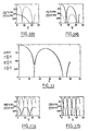
- Figures 7 to 15 illustrate the characteristics of polarization of the different components that come to be described.
- the amplitude of the TE and TM components is expressed as a function of the phase shifts of the modulators 1 and 2 (identified by the indices 1 and 2), of ⁇ 0 , and of the wave amplitudes before modulation:
- FIGS. 8a, 8b on which the amplitudes have been plotted modes depending on the modulation voltage applied to modulators 1 and 2.
- Mirror-type modulators are susceptible large-scale applications in an FTTH network.
- the insertion of a polarization converter in the modulator arm makes it insensitive to polarization. This is illustrated on Figures 14a, 14b and 15, when the arms contain two phase modulators in series with a TE converter ⁇ TM. It should be noted that in this case the optical wave crosses twice the converter and the output polarization is therefore identical to the input polarization. The effect push pull illustrated here lowers the tension extinction.
- Figure 16 illustrates an example of a modulator capacitive according to the prior art. It includes a guide optics 101 which extends linearly and which is in one electrooptical material, as well as an electrode 102 which extends over part of the length of this light guide 101. This electrode 102 allows, with metallization earthed on the other side of the guide optic 1, to generate in said optical guide 101 a electric field for the modification of its index of refraction.
- an electrooptical modulator is characterized by the product V ⁇ L, where L is the optical path traveled by light, and V ⁇ is the half-wave voltage of the modulator, i.e. the voltage necessary to apply a phase shift of ⁇ to the light wave.
- V ⁇ L ⁇ . d not 3 .r eff , where ⁇ is the operating length, d the inter-electrode distance, n the refractive index of the material forming the core, r eff the effective electrooptical coefficient.
- V ⁇ L 0.16 Vm, that is, for an operating voltage of 10 V, an optical path of 1.6 cm.
- the length of the modulator must be at least greater than 1.6 cm, to an electrode width of 10 ⁇ m.
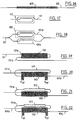
- FIG. 17 shows a modulator of phase according to a possible embodiment for the invention.
- the optical guide 111 of this modulator is folded twice on itself and has a looped shape elongate.
- the different portions of said modulator which extend juxtaposed at the level of said loop are overlapped by a metallization layer 12 which constitutes a modulator control electrode.
- a modulator configuration of the type illustrated in FIG. 17 allows, for a given value of V ⁇ , to considerably reduce the length of the modulator.
- the modulator extends over 0.5 cm, for an optical length 1.6 cm total
- the width of the electrode 112 is 200 ⁇ m.
- Such a configuration with a folded optical guide can be used to reduce the value of V ⁇ for a fixed component size.
- the optical guide 131 is folded there in a pin hair.
- An electrode 132 is superimposed on two portions 131a and 131b juxtaposed with this optical guide 31.
- modulators which have just been described in reference to Figures 17 to 19 are modulators capacitive used for command frequencies low (lower than a few GHz).
- control frequency bandwidth of such capacitive modulators is given by their constant RC, where R is their resistance and C their capacitance.
- the optical guide 141 of this modulator is in loop.
- a metallization layer 142 is superimposed linearly to two parallel portions 141a and 141b of this optical guide 141. These portions 141a and 141b are such that the optical signal propagates in the same direction.
- the metallization 142 is used as a transmission line for a microwave radio signal between an input E Rf and an output S Rf , the input E Rf being connected to a microwave source.
- the optical signal propagates in the same direction in the two portions 141a and 141b.
- the meaning of propagation of the radio signal is the same as that of optical waves, so as to allow the agreement of phase between optical waves and microwave.
- the modulator thus constituted is a modulator with progressive waves.
- ⁇ loop is greater than ⁇ electrode .
- the bandwidth of a modulator traveling wave loop is reduced compared to that of a linear modulator, and is determined by the length of the loop.
- the interest of a wave modulator progressive loop is that the line microwave is shorter than for a modulator linear, and therefore there is less power dissipated in the modulator.
- the optical guide 151 of the modulators has a intermediate portion 151a which, on said optical guide 151, is interposed between two linear portions 151b and 151c of the same length covered by the same metallization 152, said intermediate portion 151a itself not being covered by this metallization 152.
- This intermediate portion 151a has a passive TE ⁇ TM converter 153 for example of the type of that described in the article already cited above.
- a first polarization of the optical signal is modulated during the passage thereof in the input branch 151b of the modulator.
- the polarization is reversed by the passive converter 153 when passing through the branch intermediate 151a and the second polarization is modulated during the second pass under the loop, that is to say during of the optical signal passing through the output branch 151c of the modulator.
- Such a modulator therefore has the advantage of allowing to modulate the two polarizations with a single electrode.
Description
La présente invention est relative aux composants électrooptiques.The present invention relates to components electro.
Les polymères électrooptiques ont un fort potentiel dans le domaine des télécommunications. On envisage de les employer dans des réseaux de distribution optiques chez l'abonné (fiber to the home : FTTH, selon la terminologie anglo-saxonne généralement utilisée par l'Homme du Métier) car ils sont susceptibles de permettre la fabrication de composants à bas coût. Ils permettent de réaliser simplement des guides d'onde sur des substrats variés. Lorsque le polymère orienté est placé entre des électrodes, l'application d'un champ électrique de modulation entre les électrodes permet de moduler l'indice de réfraction du polymère via l'effet Pockels. Cela se traduit par un déphasage de l'onde optique guidée ; ce déphasage peut être utilisé pour traiter le signal optique (modulation, commutation, etc).Electrooptical polymers have a strong telecommunications potential. We plans to use them in distribution networks optical to the subscriber (fiber to the home: FTTH, according to Anglo-Saxon terminology generally used by the skilled person) because they are likely to allow manufacture of components at low cost. They allow to simply make waveguides on substrates varied. When the oriented polymer is placed between electrodes, applying an electric field of modulation between the electrodes modulates the index of refraction of the polymer via the Pockels effect. This is translated by a phase shift of the guided optical wave; this phase shift can be used to process the optical signal (modulation, switching, etc.).
Un but de l'invention est de proposer des perfectionnements aux composants électrooptiques connus à ce jour.An object of the invention is to propose improvements to known electrooptical components at this day.
Pour l'effet électrooptique, on distingue trois types de géométrie d'électrodes : les géométries à électrodes planes, celles à électrodes transverses et celles à électrodes coplanaires.For the electrooptical effect, there are three types of electrode geometry: geometries planar electrodes, those with transverse electrodes and those with coplanar electrodes.
Pour les géométries à électrodes planes, on forme un condensateur plan, le polymère électrooptique étant placé entre les électrodes. For geometries with planar electrodes, we form a planar capacitor, the electrooptic polymer being placed between the electrodes.
On connaít depuis longtemps des technologies permettant la réalisation de guides d'ondes à courbure.We have known for a long time technologies allowing the realization of waveguides at curvature.
On pourra à cet égard par exemple se référer à la
publication:
et plus récemment, à
and more recently, at
Toutefois, les guides optiques des composants électrooptiques connus à ce jour sont généralement quasiment rectilignes.However, the optical guides of the components electrooptics known to date are generally almost straight.
Les composants électrooptiques sont en effet habituellement fabriqués à base de cristaux ferroélectriques ou de semi-conducteurs.The electrooptical components are indeed usually made from ferroelectric crystals or semiconductors.
Or, dans de tels matériaux, le guide d'ondes est généralement réalisé par perturbation locale de l'indice de réfraction. Les différences d'indice entre le coeur et la gaine des guides étant faible (0,001), les guides optiques de ces composants doivent présenter des géométries sensiblement linéaires afin de minimiser les pertes de courbure (angle inférieur à 0,1°).However, in such materials, the waveguide is generally achieved by local disturbance of the index of refraction. The differences in index between the heart and the sheath of the guides being weak (0.001), the guides optics of these components must have substantially linear geometries to minimize loss of curvature (angle less than 0.1 °).
On notera en outre que les efforts de recherche sur ces composants portent principalement, à l'heure actuelle, sur l'optimisation des matériaux actifs, et notamment l'amélioration de leurs coefficients électrooptiques.It should also be noted that research efforts on these components relate mainly, to the hour current, on the optimization of active materials, and notably the improvement of their coefficients electro.
L'invention propose un composant comportant un guide optique dont le coeur est en un matériau électro-optique, ainsi qu'au moins une métallisation au droit d'une portion dudit guide, pour la commande de celui-ci, caractérisé en ce que le guide optique est replié et en ce que la métallisation s'étend au droit d'au moins deux portions du guide optique qui s'étendent de façon repliée l'une par rapport à l'autre.The invention provides a component comprising an optical guide whose core is in one electro-optical material, as well as at least one metallization to the right of a portion of said guide, for the control thereof, characterized in that the guide optical is folded and in that the metallization extends at least two portions of the light guide which extend folded over each other.
Le matériau électrooptique est avantageusement un matériau polymère.The electrooptical material is advantageously a polymer material.
Notamment, une telle structure trouve avantageusement application dans le cas de composants capacitifs, c'est-à-dire commandés à des fréquences inférieures ou de l'ordre du GHz, puisqu'elle permet d'en réduire la taille ou la tension de commande. On a alors un compromis tension de commande-bande passante-encombrement à optimiser.In particular, such a structure finds advantageously applied in the case of components capacitive, i.e. controlled at frequencies lower or around the GHz, since it allows reduce the size or control voltage. We then have a compromise control voltage-bandwidth-size to optimize.
Elle trouve également avantageusement application dans les composants à ondes progressives. La métallisation est alors utilisée comme ligne de transmission hyperfréquence et le signal optique se propage dans les portions de guide au droit desquelles la métallisation s'étend, dans la même direction et le même sens que le signal hyperfréquence qui se propage dans cette métallisation.It also advantageously finds application in traveling wave components. Metallization is then used as a transmission line microwave and the optical signal propagates in guide portions to the right of which the metallization extends in the same direction and the same direction as the microwave signal that propagates in this metallization.
Un tel composant présente en effet une longueur de la ligne hyperfréquence réduite, ce qui limite l'atténuation de l'onde hyperfréquence, et réduit la taille du composant.Such a component indeed has a length of the reduced microwave line, which limits attenuation of the microwave wave, and reduces the component size.
Par ailleurs, le guide optique du composant comporte avantageusement un convertisseur de polarisation disposé entre deux portions au droit desquelles s'étend la métallisation de commande.In addition, the optical guide of the component advantageously comprises a polarization converter disposed between two portions to the right of which extends the metallization control.
Une telle structure permet de moduler successivement avec une même métallisation les deux polarisations de propagation dans le guide optique ; la bande passante est réduite, mais on obtient un composant plus simple à utiliser, surtout pour la modulation hyperfréquence.Such a structure allows to modulate successively with the same metallization both propagation polarizations in the optical guide; the bandwidth is reduced, but we get a component easier to use, especially for modulation microwave.
Le composant proposé par l'invention peut être intégré monolithiquement dans tout composant optique, notamment dans un composant de Mach-Zehnder, un commutateur optique (modulateur à insertion extraction par exemple) ou tout autre composant actif utilisant l'effet électrooptique sur une portion de guide linéaire.The component proposed by the invention can be monolithically integrated into any optical component, especially in a Mach-Zehnder component, a optical switch (modulator with insertion extraction by example) or any other active component using the effect electrooptics on a linear guide portion.
D'autres caractéristiques et avantages de l'invention ressortiront encore de la description qui suit. Cette description est purement illustrative et non limitative. Elle doit être lue en regard des dessins annexés sur lesquels :
- la figure 1 est une représentation schématique d'un modulateur de phase insensible à la polarisation ;
- les figures 2 à 5 sont des représentations schématiques de modulateurs d'intensité insensibles à la polarisation ;
- la figure 6 est une représentation schématique d'un coupleur 2x2 insensible à la polarisation ;
- les figures 7a, 7b sont des graphes sur lesquels on a porté les amplitudes des modes en fonction de la tension de modulation appliquée aux modulateurs élémentaires du montage de la figure 1 ;
- les figures 8a, 8b sont des graphes sur lesquels on a porté les intensités des modes en fonction de la tension de modulation appliquée aux modulateurs élémentaires du montage de la figure 1 ;
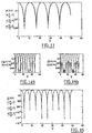
- la figure 9 est un graphe sur lequel on a porté l'intensité totale en sortie du modulateur de la figure 2 pour différents angles de polarisation d'entrée, en fonction la tension de modulation ;
- les figures 10a, 10b et 11 sont des graphes analogues à ceux des figures 8a, 8b et 9, pour le modulateur de la figure 3 ;
- les figures 12a, 12b et 13 sont des graphes analogues à ceux des figures 8a, 8b et 9, pour le modulateur de la figure 4 ;
- les figures 14a, 14b et 15 sont des graphes analogues à ceux des figures 8a, 8b et 9, pour le modulateur de la figure 5 ;
- la figure 16 illustre un modulateur conforme à un art antérieur connu ;
- les figures 17 à 22 illustrent des modulateurs conformes à différents modes de réalisation possibles pour l'invention.
- Figure 1 is a schematic representation of a phase modulator insensitive to polarization;
- Figures 2 to 5 are schematic representations of intensity modulators insensitive to polarization;
- FIG. 6 is a schematic representation of a 2x2 coupler insensitive to polarization;
- FIGS. 7a, 7b are graphs on which the amplitudes of the modes have been plotted as a function of the modulation voltage applied to the elementary modulators of the assembly of FIG. 1;
- FIGS. 8a, 8b are graphs on which the intensities of the modes have been plotted as a function of the modulation voltage applied to the elementary modulators of the assembly of FIG. 1;
- FIG. 9 is a graph on which the total intensity at the output of the modulator of FIG. 2 has been plotted for different angles of input polarization, as a function of the modulation voltage;
- Figures 10a, 10b and 11 are graphs similar to those of Figures 8a, 8b and 9, for the modulator of Figure 3;
- Figures 12a, 12b and 13 are graphs similar to those of Figures 8a, 8b and 9, for the modulator of Figure 4;
- Figures 14a, 14b and 15 are graphs similar to those of Figures 8a, 8b and 9, for the modulator of Figure 5;
- FIG. 16 illustrates a modulator according to a known prior art;
- Figures 17 to 22 illustrate modulators according to different possible embodiments for the invention.
Le modulateur de phase indépendant de la
polarisation illustré sur la figure 1 comporte deux
modulateurs de phase identiques 1 et 2 entre lesquels est
disposé un convertisseur TE TM référencé par 3.The phase modulator independent of the
polarization illustrated in Figure 1 has two
Les modulateurs 1 et 2 sont des
modulateurs électro-optiques du type de ceux qui sont
décrits plus loin de façon détaillée en référence aux
figures 16 et suivantes.
Le convertisseur TE TM est un convertisseur type de celui décrit dans la publication :
- (M. C. Oh et al., Appl. Phys. Lett 67 (13) (1995) pp 1821-1823).
- (MC Oh et al., Appl. Phys. Lett 67 (13) (1995) pp 1821-1823).
Par exemple, dans le cas de modulateurs 1 et 2 à
électrodes planes, la composante TM est d'abord modulée
via le coefficient r33 dans le premier modulateur, puis
est convertie en polarisation TE par le convertisseur,
puis est modulée via le coefficient r13 dans le deuxième
modulateur. La composante TE incidente est modulée via le
coefficient r13 dans le premier modulateur, puis est
convertie en polarisation TM par le convertisseur, puis
est modulée via le coefficient r33 dans le deuxième
modulateur. Si les deux modulateurs sont de même longueur,
l'effet de la modulation sera le même sur les deux
polarisations.For example, in the case of
Les figures 2 à 6 illustrent d'autres composants optiques insensibles à la polarisation.Figures 2 to 6 illustrate other optical components insensitive to polarization.
Le dispositif illustré sur la figure 2 est un modulateur d'intensité de type Mach-Zehnder indépendant de la polarisation.The device illustrated in Figure 2 is a intensity modulator of Mach-Zehnder type independent of polarization.
L'une de ses deux branches, référencée par 21a, comporte un montage du type de celui illustré sur la figure 1.One of its two branches, referenced by 21a, includes an assembly of the type illustrated on the figure 1.
L'autre de ses deux branches, référencée par 21b, comporte un convertisseur TE TM, référencé par 22.The other of its two branches, referenced by 21b, includes a TE TM converter, referenced by 22.
La figure 3 illustre un autre mode de réalisation possible pour un modulateur d'intensité insensible à la polarisation.Figure 3 illustrates another embodiment possible for an intensity modulator insensitive to polarization.
Ce modulateur comporte deux modulateurs 31a, 31b
d'intensité de type Mach-Zehnder classiques qui sont
montés en série et entre lesquels est disposé un
convertisseur TE TM, référencé par 32. This modulator comprises two
En variante encore, ainsi qu'illustré sur la
figure 4, on peut utiliser sur chacune des deux branches
41a, 41b d'un montage Mach-Zehnder, des modulateurs de
phase du type de celui illustré sur la figure 1. Les
modulateurs élémentaires réalisent des modulations de
phase de signes opposés.In another variant, as illustrated on the
figure 4, one can use on each of the two
On dispose ainsi d'un montage "push-pull" (selon la terminologie anglo-saxonne généralement utilisée par l'Homme du Métier) indépendant de la polarisation.We thus have a "push-pull" assembly (according to the Anglo-Saxon terminology generally used by skilled in the art) independent of polarization.
Egalement, ainsi qu'illustré sur la figure 5, le
modulateur de la figure 1 peut être utilisé sur chacune
des deux branches 51a, 51b d'un modulateur d'intensité à
miroir (1/2 Mach-Zehnder dont chaque branche 51a, 51b se
termine par un miroir 52), pour réaliser un montage "push-pull"
indépendant de la polarisation.Also, as illustrated in FIG. 5, the
Figure 1 modulator can be used on each
of the two
En variante encore, ainsi qu'illustré sur la figure 6, le dispositif de la figure 1 peut être utilisé pour réaliser des coupleurs directifs indépendants de la polarisation.In another variant, as illustrated on the Figure 6, the device of Figure 1 can be used to make directional couplers independent of the polarization.
Sur la figure 6, un montage Mach-Zehnder "push-pull"
du type de celui illustré sur la figure 4 est
disposé entre deux coupleurs directifs 61, 62, les deux
branches 63a, 63b dudit montage prolongeant les branches
de sortie du coupleur d'entrée 61 et se prolongeant par
les branches d'entrée du coupleur de sortie 62. Plus
précisément, les coupleurs directifs 3 dB sont du type
comportant deux guides d'onde qui sont juxtaposés et
s'étendent parallèlement sur une partie de leur longueur. In Figure 6, a Mach-Zehnder "push-pull" arrangement
of the type shown in Figure 4 is
disposed between two
Les figures 7 à 15 illustrent les caractéristiques de polarisation des différents composants qui viennent d'être décrits.Figures 7 to 15 illustrate the characteristics of polarization of the different components that come to be described.
Ces différentes courbes ont été obtenues en faisant l'hypothèse qu'un convertisseur TE TM module les modes TE et TM sur une distance égale à la longueur de couplage, c'est-à-dire comme un convertisseur imparfait, dont on peut prévoir les effets des imperfections sur la performance en sortie du composant.These different curves were obtained in assuming that a TE TM converter modulates TE and TM modes over a distance equal to the length of coupling, i.e. as an imperfect converter, the effects of imperfections on which can be predicted component output performance.
On définit un angle ϕ0 relié au contraste (exprimé
en dB) par :
Dans le cas d'un modulateur de phase insensible à
la polarisation, l'amplitude des composantes TE et TM
s'exprime en fonction des déphasages des modulateurs 1 et
2 (repérés par les indices 1 et 2), de ϕ0, et des
amplitudes des ondes avant modulation :

Dans le cas idéal où les déphasages induits par
les modulateurs 1 et 2 sont identiques, et où ϕ0=0
(contraste infini), on obtient une modulation de phase
indépendante de la polarisation (à laquelle s'ajoute une
conversion de polarisation) :
Dans le cas d'un convertisseur imparfait, les
termes principaux sont modulés avec la même phase, mais il
reste des modulations résiduelles sur la deuxième
composante de la polarisation. C'est ce qu'illustrent les
figures 8a, 8b, sur lesquelles on a porté les amplitudes
des modes en fonction de tension de modulation appliquée
aux modulateurs 1 et 2.In the case of an imperfect converter, the
main terms are modulated with the same phase but it
rest of the residual modulations on the second
component of polarization. This is illustrated by
FIGS. 8a, 8b, on which the amplitudes have been plotted
modes depending on the modulation voltage applied
to
Le cas d'un modulateur de Mach-Zehnder insensible à la polarisation, comportant un convertisseur TE TM imparfait (contraste de 22 dB), est illustré sur les figures 8a, 8b où on représente les intensités de chaque mode en sortie pour un mode TE ou TM en entrée. La tension d'extinction est plus faible que la tension d'extinction de chaque modulateur pris séparément, car les phases des deux modulateurs de phase s'ajoutent. On remarque que la composante résiduelle ("cross-talk"), due à l'imperfection du convertisseur, est négligeable devant la composante principale du signal.The case of an insensitive Mach-Zehnder modulator polarization, comprising a TE TM converter imperfect (22 dB contrast), is illustrated on the Figures 8a, 8b where we represent the intensities of each output mode for TE or TM input mode. Voltage is lower than the extinguishing voltage of each modulator taken separately, because the phases of two phase modulators are added. We notice that the residual component ("cross-talk"), due to imperfection of the converter, is negligible compared to the component main signal.
Sur la figure 9, on a représenté en fonction de la tension de modulation l'intensité totale en sortie pour différents angles de polarisation d'entrée (supposée linéaire pour simplifier).In Figure 9, there is shown as a function of the modulation voltage the total output intensity for different input polarization angles (assumed linear for simplicity).
Le cas de deux modulateurs de Mach-Zehnder en série avec un convertisseur de polarisation (montage de la figure 3) est illustré figures 10a, 10b et 11. Comme on le constatera sur ces figures,ce montage permet l'indépendance en polarisation, mais ce cas est plus défavorable que le cas précédent : en effet, la tension d'extinction est égale à la plus petite des tensions d'extinction, car, dans ce cas, on effectue le produit des modulations d'intensité de chaque modulateur. The case of two Mach-Zehnder modulators in series with a polarization converter (mounting the Figure 3) is illustrated in Figures 10a, 10b and 11. As we will see in these figures, this assembly allows independence in polarization but this case is more unfavorable than the previous case: indeed, the tension extinction is equal to the smallest of the voltages because, in this case, the product of intensity modulations of each modulator.
L'effet "push-pull" indépendant de la polarisation est illustré sur les figures 12a, 12b et 13 pour un modulateur de Mach-Zehnder comportant des modulateurs de phase en série avec un convertisseur de polarisation (montage de la figure 4). On obtient l'indépendance en polarisation, et une réduction d'un facteur 2 de la tension d'extinction, par rapport à un modulateur de Mach-Zehnder du type de la figure 2.The "push-pull" effect independent of polarization is illustrated in Figures 12a, 12b and 13 for a Mach-Zehnder modulator comprising modulators of phase in series with a polarization converter (assembly of figure 4). We obtain independence in polarization, and a 2-fold reduction in extinction voltage, compared to a Mach-Zehnder modulator of the type of figure 2.
Des modulateurs type miroir sont susceptibles d'applications à grande échelle dans un réseau FTTH. L'insertion d'un convertisseur de polarisation dans les bras du modulateur (figure 5) permet de le rendre insensible à la polarisation. Cela est illustré sur les figures 14a, 14b et 15, lorsque les bras contiennent deux modulateurs de phase en série avec un convertisseur TE TM. Il faut noter que dans ce cas l'onde optique traverse deux fois le convertisseur et la polarisation en sortie est donc identique à la polarisation d'entrée. L'effet push pull illustré ici permet d'abaisser la tension d'extinction.Mirror-type modulators are susceptible large-scale applications in an FTTH network. The insertion of a polarization converter in the modulator arm (figure 5) makes it insensitive to polarization. This is illustrated on Figures 14a, 14b and 15, when the arms contain two phase modulators in series with a TE converter TM. It should be noted that in this case the optical wave crosses twice the converter and the output polarization is therefore identical to the input polarization. The effect push pull illustrated here lowers the tension extinction.
On va maintenant décrire en référence aux figures 16 et suivantes des structures de commutateurs et modulateurs avantageuses. We will now describe with reference to the figures 16 and following switch structures and advantageous modulators.
La figure 16 illustre un exemple de modulateur
capacitif conforme à l'art antérieur. Il comporte un guide
optique 101 qui s'étend linéairement et qui est en un
matériau électrooptique, ainsi qu'une électrode 102 qui
s'étend sur une partie de la longueur de ce guide optique
101. Cette électrode 102 permet, avec une métallisation
reliée à la masse disposée de l'autre côté du guide
optique 1, de générer dans ledit guide optique 101 un
champ électrique pour la modification de son indice de
réfraction.Figure 16 illustrates an example of a modulator
capacitive according to the prior art. It includes a
On sait qu'un modulateur électrooptique est caractérisé par le produit VπL, où L est le chemin optique parcouru par la lumière, et Vπ est la tension demi-onde du modulateur, c'est à dire la tension nécessaire pour appliquer un déphasage de π à l'onde lumineuse.We know that an electrooptical modulator is characterized by the product V π L, where L is the optical path traveled by light, and V π is the half-wave voltage of the modulator, i.e. the voltage necessary to apply a phase shift of π to the light wave.
Dans le cas de polymères électrooptiques,
Pour λ = 1,3 µm, d = 5 µm, n = 1,6, et reff = 10 pm/V, on obtient VπL = 0,16 Vm, soit, pour une tension de fonctionnement de 10 V, un chemin optique de 1,6 cm.For λ = 1.3 µm, d = 5 µm, n = 1.6, and r eff = 10 pm / V, we obtain V π L = 0.16 Vm, that is, for an operating voltage of 10 V, an optical path of 1.6 cm.
Ainsi, dans le cas d'un modulateur conforme à l'art antérieur illustré sur la figure 16, la longueur du modulateur doit être au moins supérieure à 1,6 cm, pour une largeur d'électrode de 10 µm.Thus, in the case of a modulator conforming to prior art illustrated in Figure 16, the length of the modulator must be at least greater than 1.6 cm, to an electrode width of 10 µm.
On a représenté sur la figure 17 un modulateur de phase conforme à un mode de réalisation possible pour l'invention.FIG. 17 shows a modulator of phase according to a possible embodiment for the invention.
Le guide optique 111 de ce modulateur est replié
deux fois sur lui-même et présente une forme en boucle
allongée. Les différentes portions dudit modulateur qui
s'étendent de façon juxtaposées au niveau de ladite boucle
sont chevauchées par une couche de métallisation 12 qui
constitue une électrode de commande du modulateur.The
Le guide est conçu de manière à tolérer des courbures importantes, par exemple en choisissant pour le coeur et la gaine des matériaux ayant une différence d'indice de réfraction importante comme ceux décrits dans la publication :
- J. Liang, R. Levenson, J. Zyss, ACS/OSA 93 (Toronto) - Topical Meeting - organic Thin Films for Photonic Applications, "Design and fabrication of electro-optic polymer waveguides".
- J. Liang, R. Levenson, J. Zyss, ACS / OSA 93 (Toronto) - Topical Meeting - organic Thin Films for Photonic Applications, "Design and fabrication of electro-optic polymer waveguides".
De tels matériaux permettent en effet des rayons de courbure importants.Such materials indeed allow rays significant curvature.
En particulier, ils permettent de réaliser des guides optiques repliés.In particular, they make it possible to carry out folded optical guides.
Comme on l'aura compris, une configuration de modulateur du type de celle illustrée sur la figure 17 permet, pour une valeur de Vπ donnée, de diminuer considérablement la longueur du modulateur.As will be understood, a modulator configuration of the type illustrated in FIG. 17 allows, for a given value of V π , to considerably reduce the length of the modulator.
Notamment, pour diminuer la longueur d'un composant d'un facteur entier N, il suffit de réaliser (N-1)/2 boucles.In particular, to decrease the length of a component of an integer factor N, just realize (N-1) / 2 loops.
Ainsi, dans l'exemple qui vient d'être décrit, le modulateur s'étend sur 0,5 cm, pour une longueur optique totale de 1,6 cm,Thus, in the example which has just been described, the modulator extends over 0.5 cm, for an optical length 1.6 cm total,
La largeur de l'électrode 112 est de 200 µm.The width of the
Egalement, une telle configuration à guide optique replié peut être utilisée pour diminuer la valeur de Vπ pour une taille de composant fixée.Also, such a configuration with a folded optical guide can be used to reduce the value of V π for a fixed component size.
Ainsi, si pour une même taille de modulateur on veut réduire la tension Vπ d'un rapport N, il suffit de réaliser un composant du type de celui de la figure 17, avec (N-1)/2 boucles.Thus, if for the same modulator size we want to reduce the voltage V π by a ratio N, it suffices to make a component of the type of that of FIG. 17, with (N-1) / 2 loops.
D'autres modes de réalisation de l'invention sont bien entendu possibles.Other embodiments of the invention are of course possible.
On a par exemple illustré sur la figure 18 un
modulateur d'intensité de type Mach-zehnder dont les deux
branches 121a et 121b de guides optiques sont en boucle,
une électrode 22 étant superposée à la partie en boucle de
la branche 121a.We have for example illustrated in Figure 18 a
intensity modulator of the Mach-Zehnder type, both of which
Sur la figure 19, on a représenté une autre configuration de modulateur de phase.In Figure 19, there is shown another phase modulator configuration.
Le guide optique 131 y est replié en épingle à
cheveux.The
Une électrode 132 est superposée à deux portions
131a et 131b juxtaposées de ce guide optique 31.An
Les modulateurs qui viennent d'être décrits en référence aux figures 17 à 19 sont des modulateurs capacitifs utilisés pour des fréquences de commandes basses (inférieures à quelques GHz).The modulators which have just been described in reference to Figures 17 to 19 are modulators capacitive used for command frequencies low (lower than a few GHz).
La bande passante en fréquence de commande de tels modulateurs capacitifs est donnée par leur constante RC, où R est leur résistance et C leur capacitance.The control frequency bandwidth of such capacitive modulators is given by their constant RC, where R is their resistance and C their capacitance.
Pour un modulateur en boucle, il faut ajouter pour
déterminer cette bande passante la limitation due au
retard optique dans la boucle : pour une boucle de
longueur 1 mm, la fréquence de coupure parasite est de
l'ordre de 100 GHz. L'effet de la boucle est donc
négligeable.For a loop modulator, add for
determine this bandwidth the limitation due to
optical delay in the loop: for a loop of
Sur la figure 20, on a représenté un modulateur à ondes progressives conforme à l'invention.In Figure 20, there is shown a modulator with traveling waves according to the invention.
Le guide optique 141 de ce modulateur est en
boucle. Une couche de métallisation 142 est superposée
linéairement à deux portions parallèles 141a et 141b de ce
guide optique 141. Ces portions 141a et 141b sont telles
que le signal optique s'y propage dans le même sens.The
La métallisation 142 est utilisée comme ligne de
transmission d'un signal radio-électrique hyperfréquence
entre une entrée ERf et une sortie SRf, l'entrée ERf étant
reliée à une source hyperfréquence.The
Le signal optique se propage dans le même sens
dans les deux portions 141a et 141b. Le sens de
propagation du signal radio-électrique est le même que
celui des ondes optiques, de façon à permettre l'accord de
phase entre les ondes optiques et hyperfréquence.The optical signal propagates in the same direction
in the two
Le modulateur ainsi constitué est un modulateur à ondes progressives.The modulator thus constituted is a modulator with progressive waves.
L'efficacité de modulation est proportionnelle au
terme :
et où τboucle et τélectrode désignent respectivement les
retards optiques dus à la boucle et à l'électrode,The modulation efficiency is proportional to the term:
and where τ loop and τ electrode respectively designate the optical delays due to the loop and to the electrode,
En l'occurrence, τboucle est supérieur à τélectrode.In this case, τ loop is greater than τ electrode .
Pour un modulateur linéaire équivalent (ligne de
transmission deux fois plus longue), le coefficient
correspondant serait :
Par conséquent, la bande passante d'un modulateur à ondes progressives en boucle est réduite par rapport à celle d'un modulateur linéaire, et est déterminée par la longueur de la boucle.Therefore, the bandwidth of a modulator traveling wave loop is reduced compared to that of a linear modulator, and is determined by the length of the loop.
Néanmoins, l'intérêt d'un modulateur à ondes progressives en boucle tient en ce que la ligne hyperfréquence est plus courte que pour un modulateur linéaire, et qu'il y a par conséquent moins de puissance dissipée dans le modulateur.Nevertheless, the interest of a wave modulator progressive loop is that the line microwave is shorter than for a modulator linear, and therefore there is less power dissipated in the modulator.
On se réfère maintenant aux figures 21 et 22 sur lesquelles on a représenté des modulateurs en boucle respectivement de type capacitif et à ondes progressives, indépendants de la polarisation.We now refer to Figures 21 and 22 on which are shown loop modulators capacitive and traveling waves respectively, independent of polarization.
Le guide optique 151 des modulateurs présente une
portion intermédiaire 151a qui, sur ledit guide optique
151, est interposée entre deux portions linéaires 151b et
151c de même longueur recouvertes par une même
métallisation 152, ladite portion intermédiaire 151a
n'étant elle-même pas recouverte par cette métallisation
152.The optical guide 151 of the modulators has a
Cette portion intermédiaire 151a présente un
convertisseur TE TM passif 153 par exemple du type de
celui décrit dans l'article déjà cité précédemment.This
Avec un tel montage, une première polarisation du
signal optique est modulée lors du passage de celui-ci
dans la branche d'entrée 151b du modulateur.With such an arrangement, a first polarization of the
optical signal is modulated during the passage thereof
in the
Puis, la polarisation est inversée par le
convertisseur passif 153 lors du passage dans la branche
intermédiaire 151a et la deuxième polarisation est modulée
lors du deuxième passage sous la boucle, c'est-à-dire lors
du passage du signal optique dans la branche de sortie
151c du modulateur.Then, the polarization is reversed by the
Un tel modulateur a donc l'avantage de permettre de moduler les deux polarisations avec une seule électrode.Such a modulator therefore has the advantage of allowing to modulate the two polarizations with a single electrode.
Par conséquent, il n'est pas nécessaire de prévoir des électrodes transverses, de sorte que la fabrication est considérablement simplifiée.Therefore, it is not necessary to plan transverse electrodes, so that manufacturing is considerably simplified.
Claims (7)
- An optical component including a light guide (111, 121, 131, 141, 151) whose core is made of an electro-optical material, together with at least one area of metallization (112, 122, 132, 142, 152) over a portion of said light guide, for the purpose of controlling it, the component being characterized in that said light guide (111, 121, 131, 141, 151) is folded on itself and in that the metallization (112, 122, 132, 142, 152) extends over at least two portions of the light guide extended in folded manner relative to each other.
- A component according to claim 1, characterized in that the electro-optical material is a polymer material.
- A capacitive component according to claim 1 or 2, characterized in that the metallization (112, 122, 132, 152) is a control electrode for said component.
- A travelling wave component according to claim 1 or 2, characterized in that the metallization (142, 152) is a microwave transmission line, and in that the optical signal propagates in the portions (141a, 141b; 151b, 151c) of the light guide over which said metallization (142, 152) extends along the same axis and in the same direction as the microwave signal which propagates in said metallization.
- A component according to any one of claims 1 to 4, characterized in that the light guide (151) includes a polarization converter (153) between two portions (151b, 151c) over which the control metallization (152) extends.
- A modulation component according to any one of claims 1 to 4.
- A switching component according to any one of claims 1 to 4.
Applications Claiming Priority (2)
| Application Number | Priority Date | Filing Date | Title |
|---|---|---|---|
| FR9607528A FR2749945B1 (en) | 1996-06-18 | 1996-06-18 | ELECTROOPTIC COMPONENT |
| FR9607528 | 1996-06-18 |
Publications (3)
| Publication Number | Publication Date |
|---|---|
| EP0816896A2 EP0816896A2 (en) | 1998-01-07 |
| EP0816896A3 EP0816896A3 (en) | 1998-02-11 |
| EP0816896B1 true EP0816896B1 (en) | 2004-08-25 |
Family
ID=9493137
Family Applications (1)
| Application Number | Title | Priority Date | Filing Date |
|---|---|---|---|
| EP97401380A Expired - Lifetime EP0816896B1 (en) | 1996-06-18 | 1997-06-17 | Optical component |
Country Status (4)
| Country | Link |
|---|---|
| US (1) | US5930412A (en) |
| EP (1) | EP0816896B1 (en) |
| DE (1) | DE69730384T2 (en) |
| FR (1) | FR2749945B1 (en) |
Families Citing this family (12)
| Publication number | Priority date | Publication date | Assignee | Title |
|---|---|---|---|---|
| FR2776784A1 (en) * | 1998-03-30 | 1999-10-01 | France Telecom | Electro-optical modulator, forming a Pockels cell |
| US6337755B1 (en) * | 1998-11-17 | 2002-01-08 | Qtera Corporation | Polarization independent all-optical regenerators |
| US6148122A (en) * | 1998-11-17 | 2000-11-14 | Qtera Corporation | High speed lithium niobate polarization independent modulators |
| WO2001023955A2 (en) * | 1999-09-21 | 2001-04-05 | Nanovation Technologies, Inc. | A nanophotonic mach-zehnder interferometer switch and filter |
| EP1107488A1 (en) * | 1999-12-06 | 2001-06-13 | Qtera Corporation | Polarization independent all-optical regenerators |
| EP1109051A1 (en) * | 1999-12-06 | 2001-06-20 | Qtera Corporation | Polarisation independent optical phase modulator |
| US6512860B2 (en) * | 2000-08-18 | 2003-01-28 | Danmarks Tekniske Universitet | Bent electro-absorption modulator |
| US6760493B2 (en) * | 2001-06-28 | 2004-07-06 | Avanex Corporation | Coplanar integrated optical waveguide electro-optical modulator |
| DE60139549D1 (en) * | 2001-06-28 | 2009-09-24 | Avanex Corp | Electro-optical modulator with integrated coplanar optical waveguide |
| US6754429B2 (en) * | 2001-07-06 | 2004-06-22 | Corning Incorporated | Method of making optical fiber devices and devices thereof |
| EP1279999A1 (en) * | 2001-07-23 | 2003-01-29 | Corning Incorporated | Polarization-insensitive variable optical attenuator |
| US8173045B2 (en) | 2008-05-28 | 2012-05-08 | University Of Washington | Diels-Alder crosslinkable dendritic nonlinear optic chromophores and polymer composites |
Family Cites Families (11)
| Publication number | Priority date | Publication date | Assignee | Title |
|---|---|---|---|---|
| US3589794A (en) * | 1968-08-07 | 1971-06-29 | Bell Telephone Labor Inc | Optical circuits |
| US4384760A (en) * | 1980-12-15 | 1983-05-24 | Bell Telephone Laboratories, Incorporated | Polarization transformer |
| US4390236A (en) * | 1981-03-19 | 1983-06-28 | Bell Telephone Laboratories, Incorporated | Tunable polarization independent wavelength filter |
| US4691984A (en) * | 1985-09-26 | 1987-09-08 | Trw Inc. | Wavelength-independent polarization converter |
| GB8630959D0 (en) * | 1986-12-29 | 1987-02-04 | British Telecomm | Optical polarisation control |
| NL9200576A (en) * | 1992-03-27 | 1993-10-18 | Nederland Ptt | ADJUSTABLE POLARIZATION INVERTER. |
| JP2724098B2 (en) * | 1992-10-07 | 1998-03-09 | 沖電気工業株式会社 | Optical wavelength filter device |
| JPH07159738A (en) * | 1993-12-06 | 1995-06-23 | Hitachi Chem Co Ltd | Composition for active optical waveguide, production of active optical waveguide using the same and active optical waveguide |
| DE19549395A1 (en) * | 1995-02-07 | 1996-10-31 | Ldt Gmbh & Co | Image generation system for detecting and treating sight defects |
| NL1003198C2 (en) * | 1995-07-07 | 1997-11-25 | Nederland Ptt | Polarization-independent optical device. |
| US5654818A (en) * | 1996-02-09 | 1997-08-05 | The United States Of America As Represented By The United States National Aeronautics And Space Administration | Polarization independent electro-optic modulator |
-
1996
- 1996-06-18 FR FR9607528A patent/FR2749945B1/en not_active Expired - Fee Related
-
1997
- 1997-06-17 DE DE69730384T patent/DE69730384T2/en not_active Expired - Lifetime
- 1997-06-17 EP EP97401380A patent/EP0816896B1/en not_active Expired - Lifetime
- 1997-06-18 US US08/878,048 patent/US5930412A/en not_active Expired - Lifetime
Non-Patent Citations (1)
| Title |
|---|
| BUACHIDZE Z.E. ET AL: "Waveguide electrooptic modulator with a limiting modulation frequency higher than 10 GHz", SOV. J. QUANTUM ELECTRON., vol. 18, no. 7, 1988, NEW YORK, NY, US, pages 898 - 899, XP000054147, DOI: doi:10.1070/QE1988v018n07ABEH012322 * |
Also Published As
| Publication number | Publication date |
|---|---|
| EP0816896A3 (en) | 1998-02-11 |
| FR2749945B1 (en) | 1998-09-11 |
| EP0816896A2 (en) | 1998-01-07 |
| DE69730384T2 (en) | 2005-09-01 |
| US5930412A (en) | 1999-07-27 |
| DE69730384D1 (en) | 2004-09-30 |
| FR2749945A1 (en) | 1997-12-19 |
Similar Documents
| Publication | Publication Date | Title |
|---|---|---|
| EP0442802B1 (en) | Polarisation splitter for waveguide light | |
| EP0017571B1 (en) | Light intensity modulator in integrated optics and integrated optical circuit comprising such a modulator | |
| EP3009879B1 (en) | Electro-optical -phase modulator and modulation method | |
| EP0816896B1 (en) | Optical component | |
| FR2694817A1 (en) | Tunable interferometric optical filter. | |
| FR2502353A1 (en) | WAVE LENGTH FILTER TUNABLE AND INDEPENDENT OF POLARIZATION | |
| FR2544881A1 (en) | ELECTRO-OPTICAL DEVICE WITH PROGRESSIVE WAVES | |
| EP0869377B1 (en) | Integrated optical element with polarization effect | |
| EP0788017B1 (en) | Polarization independent nonlinear optical loop mirror (NOLM) | |
| FR2695216A1 (en) | Optical switch having a propagation direction close to the Z axis of the electro-optical material. | |
| US20170293083A1 (en) | Optical loop enhanced optical modulators | |
| EP1412814B1 (en) | Wide band electro-optical modulators | |
| Nelan et al. | Compact thin film lithium niobate folded intensity modulator using a waveguide crossing | |
| EP0374006A1 (en) | Optical frequency translator and modulator using such a device | |
| FR2598823A1 (en) | DIRECTIONAL OPTOELECTRONIC COUPLER FOR NON POLARIZED CONTROL SIGNAL. | |
| FR2743234A1 (en) | WAVE LENGTH DEMULTIPLEXER | |
| EP0099282B1 (en) | Polarization-independent integrated optical modulator | |
| EP0591301B1 (en) | Integrated electrooptic modulation device | |
| US6757091B1 (en) | Method and apparatus for phase shifting an optical beam in an optical device | |
| EP0094866B1 (en) | Bidirectional link arrangement of the single-mode optical fibre bus type | |
| EP0783127B1 (en) | Mach-Zehner interferometric coupler with single-mode optical fibre | |
| US11289877B2 (en) | Optical system and method for locking a wavelength of a tunable laser | |
| EP0125182B1 (en) | Alternate dephasing electro-optical directional coupler with three electrodes | |
| EP0299842B1 (en) | Electrooptic integrated modulator-commutator with bandpass response | |
| Gill et al. | Optical modulation techniques for analog signal processing and CMOS compatible electro-optic modulation |
Legal Events
| Date | Code | Title | Description |
|---|---|---|---|
| PUAI | Public reference made under article 153(3) epc to a published international application that has entered the european phase |
Free format text: ORIGINAL CODE: 0009012 |
|
| PUAL | Search report despatched |
Free format text: ORIGINAL CODE: 0009013 |
|
| AK | Designated contracting states |
Kind code of ref document: A2 Designated state(s): DE FR GB |
|
| AK | Designated contracting states |
Kind code of ref document: A3 Designated state(s): AT BE CH DE DK ES FI FR GB GR IE IT LI LU MC NL PT SE |
|
| 17P | Request for examination filed |
Effective date: 19980803 |
|
| AKX | Designation fees paid |
Free format text: DE FR GB |
|
| RBV | Designated contracting states (corrected) |
Designated state(s): DE FR GB |
|
| 17Q | First examination report despatched |
Effective date: 20030725 |
|
| GRAP | Despatch of communication of intention to grant a patent |
Free format text: ORIGINAL CODE: EPIDOSNIGR1 |
|
| GRAS | Grant fee paid |
Free format text: ORIGINAL CODE: EPIDOSNIGR3 |
|
| GRAA | (expected) grant |
Free format text: ORIGINAL CODE: 0009210 |
|
| AK | Designated contracting states |
Kind code of ref document: B1 Designated state(s): DE FR GB |
|
| REG | Reference to a national code |
Ref country code: GB Ref legal event code: FG4D Free format text: NOT ENGLISH |
|
| GBT | Gb: translation of ep patent filed (gb section 77(6)(a)/1977) |
Effective date: 20040818 |
|
| REF | Corresponds to: |
Ref document number: 69730384 Country of ref document: DE Date of ref document: 20040930 Kind code of ref document: P |
|
| PLBE | No opposition filed within time limit |
Free format text: ORIGINAL CODE: 0009261 |
|
| STAA | Information on the status of an ep patent application or granted ep patent |
Free format text: STATUS: NO OPPOSITION FILED WITHIN TIME LIMIT |
|
| 26N | No opposition filed |
Effective date: 20050526 |
|
| REG | Reference to a national code |
Ref country code: GB Ref legal event code: 732E Free format text: REGISTERED BETWEEN 20090528 AND 20090603 |
|
| REG | Reference to a national code |
Ref country code: FR Ref legal event code: TP |
|
| PGFP | Annual fee paid to national office [announced via postgrant information from national office to epo] |
Ref country code: DE Payment date: 20110630 Year of fee payment: 15 |
|
| PGFP | Annual fee paid to national office [announced via postgrant information from national office to epo] |
Ref country code: FR Payment date: 20120614 Year of fee payment: 16 |
|
| REG | Reference to a national code |
Ref country code: DE Ref legal event code: R119 Ref document number: 69730384 Country of ref document: DE Effective date: 20130101 |
|
| PG25 | Lapsed in a contracting state [announced via postgrant information from national office to epo] |
Ref country code: DE Free format text: LAPSE BECAUSE OF NON-PAYMENT OF DUE FEES Effective date: 20130101 |
|
| REG | Reference to a national code |
Ref country code: FR Ref legal event code: ST Effective date: 20140228 |
|
| PG25 | Lapsed in a contracting state [announced via postgrant information from national office to epo] |
Ref country code: FR Free format text: LAPSE BECAUSE OF NON-PAYMENT OF DUE FEES Effective date: 20130701 |
|
| PGFP | Annual fee paid to national office [announced via postgrant information from national office to epo] |
Ref country code: GB Payment date: 20140527 Year of fee payment: 18 |
|
| GBPC | Gb: european patent ceased through non-payment of renewal fee |
Effective date: 20150617 |
|
| PG25 | Lapsed in a contracting state [announced via postgrant information from national office to epo] |
Ref country code: GB Free format text: LAPSE BECAUSE OF NON-PAYMENT OF DUE FEES Effective date: 20150617 |