EP0815529B1 - Connecteur pour appareil lecteur de carte a microcircuit - Google Patents
Connecteur pour appareil lecteur de carte a microcircuit Download PDFInfo
- Publication number
- EP0815529B1 EP0815529B1 EP96908168A EP96908168A EP0815529B1 EP 0815529 B1 EP0815529 B1 EP 0815529B1 EP 96908168 A EP96908168 A EP 96908168A EP 96908168 A EP96908168 A EP 96908168A EP 0815529 B1 EP0815529 B1 EP 0815529B1
- Authority
- EP
- European Patent Office
- Prior art keywords
- card
- contact
- brush
- connector
- potential
- Prior art date
- Legal status (The legal status is an assumption and is not a legal conclusion. Google has not performed a legal analysis and makes no representation as to the accuracy of the status listed.)
- Expired - Lifetime
Links
Images


Classifications
-
- G—PHYSICS
- G06—COMPUTING; CALCULATING OR COUNTING
- G06K—GRAPHICAL DATA READING; PRESENTATION OF DATA; RECORD CARRIERS; HANDLING RECORD CARRIERS
- G06K7/00—Methods or arrangements for sensing record carriers, e.g. for reading patterns
- G06K7/06—Methods or arrangements for sensing record carriers, e.g. for reading patterns by means which conduct current when a mark is sensed or absent, e.g. contact brush for a conductive mark
-
- G—PHYSICS
- G06—COMPUTING; CALCULATING OR COUNTING
- G06K—GRAPHICAL DATA READING; PRESENTATION OF DATA; RECORD CARRIERS; HANDLING RECORD CARRIERS
- G06K7/00—Methods or arrangements for sensing record carriers, e.g. for reading patterns
- G06K7/0013—Methods or arrangements for sensing record carriers, e.g. for reading patterns by galvanic contacts, e.g. card connectors for ISO-7816 compliant smart cards or memory cards, e.g. SD card readers
- G06K7/0056—Methods or arrangements for sensing record carriers, e.g. for reading patterns by galvanic contacts, e.g. card connectors for ISO-7816 compliant smart cards or memory cards, e.g. SD card readers housing of the card connector
- G06K7/0069—Methods or arrangements for sensing record carriers, e.g. for reading patterns by galvanic contacts, e.g. card connectors for ISO-7816 compliant smart cards or memory cards, e.g. SD card readers housing of the card connector including means for detecting correct insertion of the card, e.g. end detection switches notifying that the card has been inserted completely and correctly
-
- G—PHYSICS
- G06—COMPUTING; CALCULATING OR COUNTING
- G06K—GRAPHICAL DATA READING; PRESENTATION OF DATA; RECORD CARRIERS; HANDLING RECORD CARRIERS
- G06K7/00—Methods or arrangements for sensing record carriers, e.g. for reading patterns
- G06K7/0013—Methods or arrangements for sensing record carriers, e.g. for reading patterns by galvanic contacts, e.g. card connectors for ISO-7816 compliant smart cards or memory cards, e.g. SD card readers
- G06K7/0021—Methods or arrangements for sensing record carriers, e.g. for reading patterns by galvanic contacts, e.g. card connectors for ISO-7816 compliant smart cards or memory cards, e.g. SD card readers for reading/sensing record carriers having surface contacts
Definitions
- the invention relates to a connector for a card reader device. microcircuit.
- the term “card” means all kinds of cards of the type incorporating a monolithic or hybrid integrated circuit, known as a "chip".
- This term “microcircuit” will be used in the following. This is, for example, format card “credit card”, also known under the name “CAM” (Carte A Mémoire "). Most often, the microcircuit is produced on the basis of a microprocessor or a microcontroller, comprising, in particular memory circuits, for example of "PROM” type. This type of card must be able to be inserted into devices specific reading and / or writing of data. To simplify this device will called “reader” in the following, it being understood that it can also ensure writing data and other related functions (power supply electrical, tests) which will be recalled below.
- the data is stored in the aforementioned memory circuits, generally in encrypted form. They are therefore read at from memory positions or on the contrary written in these memory positions.
- the first category consists of detection systems electronic.
- an electrical test is carried out, for example the resistance measurement between the brush contacts. If these tests do not match expected values, in a given range, it is deduced from this that the card is inserted incorrectly or that an object stranger is introduced in his place.
- the second category consists of so-called "to landing".
- An example of such a system is described in the patent application French FR-A-2 628 901.
- the card is positioned against a stop before contacting the brushes. Contact is made by relative displacement from the card to the brushes, perpendicular to the surface of the card (faces main).
- Safety can only be ensured by the proper functioning of mechanical organs of the system. They can however be doubled by a typical contact "limit switch” which blocks the power-up sequence in case the card does not would not be in the correct position.
- a power-up sequence can be ensured by the height of the brushes, or by an initialization of the electronics by closing of a "card presence” contact.
- the main drawback is that the arrangement mechanics required to perform the above functions is complex and expensive.
- the third category consists of brush contact systems rubbing with "limit switch" contact. Such a system is disclosed, for example, by French patent application FR-A-2 623 314.
- the connectors in which are cards inserted have a "limit switch” contact which triggers the bet on the microcircuit when the card is in the correct position.
- the mechanical arrangement is simple and inexpensive.
- the invention sets itself the goal to provide a solution to the problems mentioned above, while alleviating the drawbacks of known art systems, some of which have just been mentioned.
- the reading frame according to the invention thus comprises in combination, an electronic circuit as described in the patent application WO-A-96/24 111, as well as a brush contact additional, as described in EP-A-0 595 305.
- this brush contact instead of being additional, is a single contact element assigned to one of said ranges of contact which is offset from the brush contacts assigned to the other ranges of contact.
- the connector 1 for a microcircuit card reader device C 3 comprises a body 2 supporting brush contact elements B, intended to be brought into electrical contact with conductive pads associated with said microcircuit I C when the card C is inserted in connector 1.
- this connector 1 comprises an electronic circuit I C connected, on the one hand, with at least part of said brush contact elements C 1 to C 8 and, on the other hand, with the electronic circuit 4 of the card reader.
- the electronic circuit I C carried by the connector 1 comprises means which are detailed in PCT application No. FR 96/00156 for controlling operations of insertion or removal of the card C in the card reader.
- FIG. 2 illustrates a fragment of card C conforming to standard ISO 7816.
- This standard prescribes the dimensions, the location and the allocation of the contact pads, C 1 to C 8 , flush with the surface of microcircuit type cards. ID-1.
- the card can include one or more microcircuits. The input-output terminals of these microcircuits are connected to these contact pads, C 1 to C 8 .
- the contact pads, C 1 to C 8 are organized in two rows of four pads, respectively C 1 to C 4 and C 5 to C 8 , substantially parallel to each other and parallel to the left edge B G (in the figure) of card C, edge serving as a stop.
- the figure also represents the upper edge B S of the card C.
- the main geometric characteristics defining the contacts, C 1 to C 8 expressed in minimum and maximum distances (in mm) such as 'they appear from the above-mentioned standard.
- each conductive zone must include a substantially rectangular surface with minimum dimensions 1.7 ⁇ 2mm. Maximum dimensions are not specified. It is only indicated that each contact must be electrically isolated from the other contacts.
- the surface of the card C, between contact areas C 1 to C 8 can be insulating or conductive: for example covered with a metallization connected to the ground contact, for the purpose of decoupling.
- FIG. 3 illustrates an example of a microcircuit card C, in accordance with the AFNOR standard, older, under the same representation conditions as the card C.
- the contact C 8 in the case of the ISO card, is in place of the contact C 1 , in the case of the AFNOR card.
- the connector used in the card reader must take into account the standard used, this constraint being common to known art connectors.
- the edges of the pads of the "signal" contacts (that is to say other than C 1 and C 5 ) are aligned with the pads of contacts C 1 / C 5 or offset in the favorable direction, which is the most general case.
- FIG. 4 which again represents a card C conforming to the aforementioned ISO standard.
- the contact area C 1 supply voltage
- the contact area C 1 has an elongated shape and extends in the direction of the area C 5 .
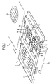
- Figures Sa and 5b represent, by way of example, an Art Connu connector, designated under the general reference 60, seen in section BB and high, respectively.
- the contact elements forming brushes, shown under the general reference 50 and folded at 63, are arranged in two rows in lights 66 and 67, respectively. It also has a pair of elements of contacts 20-30, called "limit switch" detection, folded at 60 and 61. These elements 20 and 30 are arranged in a hole 68 and their ends folded in a 68 'light.
- the front edge 70 (top of FIG. 5b), which is curved, has two lateral end points 71. These two points 71 define a stop line BB for the card.
- the region 24 of the contact element 20, located near the stop line BB has a butt-shaped profile.
- the invention is capable of two main embodiments.
- a contact element is added additional of the type “tension brushes”, which comes in parallel with the “brushes of voltage "normal, according to a configuration which will be described below.
- This brushes additional is notably offset from the normal brush.
- the contact element of the type "tension brushes" is not doubled but only offset from the row contact elements to which it belongs.
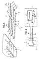
- FIG. 6 schematically illustrates a connector 1 for inserting card C according to the first embodiment of the invention.
- the card C to be inserted in the connector 1 meets the aforementioned ISO standard.
- FIG. 6 For clarity, only FIG. 6 have been shown in FIG. of contact and their arrangements in space.
- body of the connector and other accessories may be fully common to connectors of Known Art, for example to the connector shown in Figures 5a and 5b.
- the connector 1 comprises two rows of contact elements, forming brushes, respectively B C1 B C4 and B C5 -B C8 , four in each row.
- Each of these brushes is intended to be brought into galvanic contact with a corresponding area, C 1 to C 8 , of the card C. They play the role of the contact elements 50 of FIG. 5a.
- a pair of contact elements, B fc1 and B fc2 called “limit switches ", intended to detect the complete and correct insertion of the card C into the connector 1 can be provided. .
- the brushes, B C1 -B C4 and B C5 -B C8 are made of metal blades, thin and flexible, whose distal ends 10 to 80 have the shape of a stick. These blades are parallel to each other and the aforementioned distal ends are arranged opposite, two by two, on either side of an axis of symmetry A perpendicular to the blades.
- an additional contact element referenced B CX, is provided , doubling the contact element B C1 , of the "tension brushes" type.
- This additional contact element B CX can moreover be cut out ( at the time of manufacture of the connector) in the same strip as the normal contacts and overmolded at the same time as them in the body of the connector (see Figure 5b). It will be advantageous, in this case, to narrow the width of a blade and add a fifth next.
- This additional contact element B CX makes it possible to detect the insertion, as the removal of the card C and, therefore, to connect or cut the electrical energy supply, as will be explained below.
- FIG. 7a illustrates the position of the brush contact elements B C1 and B CX , with respect to the range C 1 , in the normal working position, that is to say ie card C correctly inserted in connector 1.
- the brush contact element B CX is in front of the brush contact element B C1 , but outside the range C 1 .
- the brush contact element B C1 is supplied by the supply voltage V CC , generally + 5 V.
- the range C 1 is then also brought to this potential and the microcircuit of the card C (not shown) supplied with electrical energy. Read and / or read operations can take place normally.
- FIG. 8 schematically illustrates, in the form of a block diagram, an electronic circuit for managing the state of the contact elements B C1 and B CX .
- the contact element B C1 is connected to the output V CC of a regulated electrical supply 2 disposed in the reader L.
- the additional contact element B CX is connected to the input of a circuit 3, comprising for example a voltage comparator, between V CC and a reference voltage V ref , for example 0 V, the range M being assumed to be grounded. In reality any reference voltage may be suitable, the role of the comparison circuit 3 being to detect a variation in the potential of the additional contact element B CX , of amplitude greater than a determined threshold. This threshold takes into account, in particular, the tolerances of the supply voltage, foreseeable noise, etc.
- the power supply 2 is provided with electronic circuits detecting a short-circuiting of the output (earthing of the voltage V DC ) and cutting it off. This operation will be performed for the detection of the event "a /" recalled above: detection of a short circuit.
- the detection of the event "b /" (modification of the potential of the additional brush contact element B CX ) is carried out by the comparator circuit 3.
- the output signal V S is transmitted on an input of the supply 2 and blocks this (switching off the brush contact element B C1 ) when a potential change of predetermined amplitude is detected.
- This output signal V S can also be transmitted to an electronic system to deactivate the signal brushes.
- FIG. 7c also illustrates a situation of withdrawal of the card C arte , but in this example, the mass range M (FIGS. 7a and 7b) does not exist.
- the comparator 3 FIG. 8
- the additional contact element B CX goes to the potential V CC .
- FIG. 9a illustrates the configuration to be adopted for the case of a card C according to the AFNOR standard.
- the stop (not shown) is on the side opposite the range C 1 . More specifically, this figure illustrates the normal working state.
- the additional contact element C BX is offset in front of the contact element C B1 , but rests on the pad C 1 .
- the two contact elements C BX and C B1 are therefore brought to the same potential V CC . It is also assumed that a mass range, formed by the range C 5 , adjoins the range C 1 .
- the mass range C 5 will approach the additional contact element C BX , as illustrated in FIG. 9b.
- the contact element B C1 is offset on the abutment side with respect to the contact elements of the "signal brushes" type. If we refer again to Figures 9a to 9c, we have the contact element B C1 in place of the additional contact element B CX .
- This arrangement ensures correct sequencing, by cutting the power supply, possibly after it has been short-circuited.
- the main advantage of the second embodiment is naturally that it is not necessary to provide electronics for managing the state of the brushes. In addition, only a slight modification of the contact element B C1 is necessary.
- the center of the range C 1 is at a distance equal to 18.87 mm from the stop card b, with a tolerance of +0.4 mm maximum and -0.5 mm maximum.
- the width of the range C 1 in a direction parallel to F R , is at least 2 mm and the distance separating a range contiguous to C 1 and C 1 is 0.2 mm.
- the space requirement may be less than that of the connectors equivalents of known art, because the contact elements of the "limit switch" type can be omitted, which allows a possible reduction in thickness.
Landscapes
- Engineering & Computer Science (AREA)
- Artificial Intelligence (AREA)
- Computer Vision & Pattern Recognition (AREA)
- Physics & Mathematics (AREA)
- General Physics & Mathematics (AREA)
- Theoretical Computer Science (AREA)
- Coupling Device And Connection With Printed Circuit (AREA)
- Details Of Connecting Devices For Male And Female Coupling (AREA)
Applications Claiming Priority (3)
| Application Number | Priority Date | Filing Date | Title |
|---|---|---|---|
| FR9503346 | 1995-03-22 | ||
| FR9503346 | 1995-03-22 | ||
| PCT/FR1996/000428 WO1996029672A1 (fr) | 1995-03-22 | 1996-03-21 | Connecteur pour appareil lecteur de carte a microcircuit |
Publications (2)
| Publication Number | Publication Date |
|---|---|
| EP0815529A1 EP0815529A1 (fr) | 1998-01-07 |
| EP0815529B1 true EP0815529B1 (fr) | 1999-06-23 |
Family
ID=9477296
Family Applications (1)
| Application Number | Title | Priority Date | Filing Date |
|---|---|---|---|
| EP96908168A Expired - Lifetime EP0815529B1 (fr) | 1995-03-22 | 1996-03-21 | Connecteur pour appareil lecteur de carte a microcircuit |
Country Status (11)
| Country | Link |
|---|---|
| US (1) | US5945662A (ko) |
| EP (1) | EP0815529B1 (ko) |
| JP (1) | JPH11502338A (ko) |
| KR (1) | KR19980703178A (ko) |
| AT (1) | ATE181608T1 (ko) |
| AU (1) | AU702185B2 (ko) |
| CA (1) | CA2212951C (ko) |
| DE (1) | DE69603018T2 (ko) |
| ES (1) | ES2132903T3 (ko) |
| RU (1) | RU2150744C1 (ko) |
| WO (1) | WO1996029672A1 (ko) |
Families Citing this family (10)
| Publication number | Priority date | Publication date | Assignee | Title |
|---|---|---|---|---|
| US6168082B1 (en) * | 1997-06-30 | 2001-01-02 | The Whitaker Corporation | Card reader assembly |
| FR2767592B1 (fr) * | 1997-08-20 | 1999-10-01 | Schlumberger Ind Sa | Procede de detection de fraude des cartes a memoire electronique utilisees en telephonie |
| JP3333481B2 (ja) * | 1999-11-16 | 2002-10-15 | 山一電機株式会社 | カードコネクタのカード認識スイッチ |
| US6508673B2 (en) | 2000-04-05 | 2003-01-21 | Mcdowell Jennifer Lyn | Low cost smart card reader, extension style, with wiping contacts |
| JP4436962B2 (ja) * | 2000-05-31 | 2010-03-24 | 京セラエルコ株式会社 | カード挿入検知装置 |
| JP4562199B2 (ja) * | 2007-04-09 | 2010-10-13 | 日本航空電子工業株式会社 | カード用コネクタ |
| DE102007022210B3 (de) * | 2007-05-11 | 2008-12-18 | Iprm Intellectual Property Rights Management Ag | Mehrstufiges Verbindersystem für medizinische Verwendung |
| KR20080106731A (ko) * | 2007-06-04 | 2008-12-09 | 타이코에이엠피 주식회사 | 카드 검출장치 및 그 방법 |
| US20100082466A1 (en) * | 2008-09-26 | 2010-04-01 | Mark Carlson | Beneficiary initiated p2p, p2b payment model |
| KR101679430B1 (ko) * | 2010-09-30 | 2016-11-25 | 삼성전자주식회사 | 휴대단말기에서 심카드의 삽입을 인식하는 방법 및 장치 |
Family Cites Families (8)
| Publication number | Priority date | Publication date | Assignee | Title |
|---|---|---|---|---|
| US4017834A (en) * | 1973-05-04 | 1977-04-12 | Cuttill William E | Credit card construction for automatic vending equipment and credit purchase systems |
| US4004133A (en) * | 1974-12-30 | 1977-01-18 | Rca Corporation | Credit card containing electronic circuit |
| US4575703A (en) * | 1982-07-22 | 1986-03-11 | Sony Corporation | Data reading device for data processing apparatus |
| FR2554260B1 (fr) * | 1983-10-27 | 1987-10-30 | Flonic Sa | Appareil de lecture de cartes a memoire electronique |
| FR2623314B1 (fr) * | 1987-11-13 | 1991-06-14 | Cit Alcatel | Cadre de contact pour lecteur de carte a puce, avec contact de fin de course |
| US5031599A (en) * | 1988-05-11 | 1991-07-16 | Cruise Billy J | Attachment of bowstring and cables to compound bow |
| JPH0255355U (ko) * | 1988-10-11 | 1990-04-20 | ||
| JPH06139414A (ja) * | 1992-10-28 | 1994-05-20 | Sony Corp | Icカード検出装置 |
-
1996
- 1996-03-21 US US08/913,395 patent/US5945662A/en not_active Expired - Fee Related
- 1996-03-21 AT AT96908168T patent/ATE181608T1/de not_active IP Right Cessation
- 1996-03-21 JP JP8528144A patent/JPH11502338A/ja active Pending
- 1996-03-21 CA CA002212951A patent/CA2212951C/fr not_active Expired - Fee Related
- 1996-03-21 ES ES96908168T patent/ES2132903T3/es not_active Expired - Lifetime
- 1996-03-21 KR KR1019970706581A patent/KR19980703178A/ko not_active Application Discontinuation
- 1996-03-21 DE DE69603018T patent/DE69603018T2/de not_active Expired - Fee Related
- 1996-03-21 RU RU97117346/09A patent/RU2150744C1/ru not_active IP Right Cessation
- 1996-03-21 AU AU51504/96A patent/AU702185B2/en not_active Ceased
- 1996-03-21 WO PCT/FR1996/000428 patent/WO1996029672A1/fr not_active Application Discontinuation
- 1996-03-21 EP EP96908168A patent/EP0815529B1/fr not_active Expired - Lifetime
Also Published As
| Publication number | Publication date |
|---|---|
| ES2132903T3 (es) | 1999-08-16 |
| DE69603018D1 (de) | 1999-07-29 |
| KR19980703178A (ko) | 1998-10-15 |
| AU5150496A (en) | 1996-10-08 |
| AU702185B2 (en) | 1999-02-18 |
| JPH11502338A (ja) | 1999-02-23 |
| CA2212951A1 (fr) | 1996-09-26 |
| EP0815529A1 (fr) | 1998-01-07 |
| RU2150744C1 (ru) | 2000-06-10 |
| US5945662A (en) | 1999-08-31 |
| ATE181608T1 (de) | 1999-07-15 |
| DE69603018T2 (de) | 1999-10-21 |
| WO1996029672A1 (fr) | 1996-09-26 |
| CA2212951C (fr) | 2003-02-18 |
Similar Documents
| Publication | Publication Date | Title |
|---|---|---|
| EP0815528B1 (fr) | Cadre de lecture pour appareil lecteur de carte a microcircuit | |
| EP0552078B1 (fr) | Carte enfichable pour microordinateur formant lecteur de carte à contacts affleurants | |
| EP1327222B1 (fr) | Lecteur de circuit integre sans contact | |
| EP0815529B1 (fr) | Connecteur pour appareil lecteur de carte a microcircuit | |
| EP1200927B1 (fr) | Lecteur de carte a puce comprenant un systeme d'economie d'energie | |
| EP0807295B1 (fr) | Connecteur pour appareil lecteur de carte a microcircuit et lecteur de carte comprenant un tel connecteur | |
| FR2710996A1 (fr) | Carte portable multi-applications pour ordinateur personnel. | |
| FR2533047A1 (fr) | Carte a memoire avec un circuit integre incorpore | |
| EP0262036B2 (fr) | Système de traitement d'informations à cartes à mémoire ayant plusieurs modules électroniques | |
| FR2734071A1 (fr) | Carte de paiement electronique a module interchangeable | |
| FR2808608A1 (fr) | Carte a memoire electronique destinee a etre introduite dans un dispositif de traitement | |
| FR2554262A1 (fr) | Dispositif anti-fraude pour lecteur de cartes a memoire electronique | |
| EP1116179A1 (fr) | Carte a puce sans contact comportant des moyens d'inhibition | |
| EP0349412A1 (fr) | Support d'informations et système de gestion de tels supports | |
| EP0926619B1 (fr) | Interface de communication avec une carte à puce et dispositif équipé d'une telle interface | |
| EP2791859B1 (fr) | Dispositif de décharge électrostatique | |
| FR2741976A1 (fr) | Carte amovible enfichable, formant lecteur de carte a puce pour micro-ordinateur | |
| EP0231409B1 (fr) | Lecteur de cartes | |
| FR2610430A1 (fr) | Carte a circuit integre du type a lecture sans contact avec fonction de pre-amelioration | |
| EP1053531A1 (fr) | Dispositif a circuit integre securise par attenuation de signatures electriques | |
| EP2239691A1 (fr) | Ensemble à clé mémoire comprenant une carte à microcircuit | |
| WO1996042063A1 (fr) | Carte amovible a connecteur enfichable, formant lecteur de carte a puce pour micro-ordinateur | |
| FR2948794A1 (fr) | Carte a microcircuit comprenant au moins deux interfaces externes de contacts | |
| FR2659767A1 (fr) | Circuit de caracterisation de microcircuits, lecteur enregistreur de carte a microcircuits, et carte a microcircuits associee. | |
| FR2745932A1 (fr) | Ticket a contacts et lecteur associe |
Legal Events
| Date | Code | Title | Description |
|---|---|---|---|
| PUAI | Public reference made under article 153(3) epc to a published international application that has entered the european phase |
Free format text: ORIGINAL CODE: 0009012 |
|
| 17P | Request for examination filed |
Effective date: 19970812 |
|
| AK | Designated contracting states |
Kind code of ref document: A1 Designated state(s): AT BE CH DE ES FR GB IT LI NL SE |
|
| GRAG | Despatch of communication of intention to grant |
Free format text: ORIGINAL CODE: EPIDOS AGRA |
|
| 17Q | First examination report despatched |
Effective date: 19980720 |
|
| GRAG | Despatch of communication of intention to grant |
Free format text: ORIGINAL CODE: EPIDOS AGRA |
|
| GRAH | Despatch of communication of intention to grant a patent |
Free format text: ORIGINAL CODE: EPIDOS IGRA |
|
| GRAH | Despatch of communication of intention to grant a patent |
Free format text: ORIGINAL CODE: EPIDOS IGRA |
|
| GRAA | (expected) grant |
Free format text: ORIGINAL CODE: 0009210 |
|
| AK | Designated contracting states |
Kind code of ref document: B1 Designated state(s): AT BE CH DE ES FR GB IT LI NL SE |
|
| REF | Corresponds to: |
Ref document number: 181608 Country of ref document: AT Date of ref document: 19990715 Kind code of ref document: T |
|
| REG | Reference to a national code |
Ref country code: CH Ref legal event code: NV Representative=s name: SCHMAUDER & PARTNER AG PATENTANWALTSBUERO Ref country code: CH Ref legal event code: EP |
|
| GBT | Gb: translation of ep patent filed (gb section 77(6)(a)/1977) |
Effective date: 19990630 |
|
| REF | Corresponds to: |
Ref document number: 69603018 Country of ref document: DE Date of ref document: 19990729 |
|
| REG | Reference to a national code |
Ref country code: ES Ref legal event code: FG2A Ref document number: 2132903 Country of ref document: ES Kind code of ref document: T3 |
|
| ITF | It: translation for a ep patent filed |
Owner name: STUDIO TORTA S.R.L. |
|
| PLBE | No opposition filed within time limit |
Free format text: ORIGINAL CODE: 0009261 |
|
| STAA | Information on the status of an ep patent application or granted ep patent |
Free format text: STATUS: NO OPPOSITION FILED WITHIN TIME LIMIT |
|
| 26N | No opposition filed | ||
| REG | Reference to a national code |
Ref country code: GB Ref legal event code: IF02 |
|
| PGFP | Annual fee paid to national office [announced via postgrant information from national office to epo] |
Ref country code: AT Payment date: 20020218 Year of fee payment: 7 |
|
| PG25 | Lapsed in a contracting state [announced via postgrant information from national office to epo] |
Ref country code: AT Free format text: LAPSE BECAUSE OF NON-PAYMENT OF DUE FEES Effective date: 20030321 |
|
| PGFP | Annual fee paid to national office [announced via postgrant information from national office to epo] |
Ref country code: ES Payment date: 20050214 Year of fee payment: 10 |
|
| PGFP | Annual fee paid to national office [announced via postgrant information from national office to epo] |
Ref country code: SE Payment date: 20050311 Year of fee payment: 10 |
|
| PGFP | Annual fee paid to national office [announced via postgrant information from national office to epo] |
Ref country code: CH Payment date: 20050322 Year of fee payment: 10 |
|
| PGFP | Annual fee paid to national office [announced via postgrant information from national office to epo] |
Ref country code: BE Payment date: 20050323 Year of fee payment: 10 |
|
| PGFP | Annual fee paid to national office [announced via postgrant information from national office to epo] |
Ref country code: NL Payment date: 20050331 Year of fee payment: 10 |
|
| PG25 | Lapsed in a contracting state [announced via postgrant information from national office to epo] |
Ref country code: SE Free format text: LAPSE BECAUSE OF NON-PAYMENT OF DUE FEES Effective date: 20060322 Ref country code: ES Free format text: LAPSE BECAUSE OF NON-PAYMENT OF DUE FEES Effective date: 20060322 |
|
| PG25 | Lapsed in a contracting state [announced via postgrant information from national office to epo] |
Ref country code: LI Free format text: LAPSE BECAUSE OF NON-PAYMENT OF DUE FEES Effective date: 20060331 Ref country code: CH Free format text: LAPSE BECAUSE OF NON-PAYMENT OF DUE FEES Effective date: 20060331 Ref country code: BE Free format text: LAPSE BECAUSE OF NON-PAYMENT OF DUE FEES Effective date: 20060331 |
|
| PGFP | Annual fee paid to national office [announced via postgrant information from national office to epo] |
Ref country code: IT Payment date: 20060331 Year of fee payment: 11 |
|
| PG25 | Lapsed in a contracting state [announced via postgrant information from national office to epo] |
Ref country code: NL Free format text: LAPSE BECAUSE OF NON-PAYMENT OF DUE FEES Effective date: 20061001 |
|
| REG | Reference to a national code |
Ref country code: CH Ref legal event code: PL |
|
| EUG | Se: european patent has lapsed | ||
| NLV4 | Nl: lapsed or anulled due to non-payment of the annual fee |
Effective date: 20061001 |
|
| PGFP | Annual fee paid to national office [announced via postgrant information from national office to epo] |
Ref country code: GB Payment date: 20070202 Year of fee payment: 12 |
|
| PGFP | Annual fee paid to national office [announced via postgrant information from national office to epo] |
Ref country code: DE Payment date: 20070330 Year of fee payment: 12 |
|
| REG | Reference to a national code |
Ref country code: ES Ref legal event code: FD2A Effective date: 20060322 |
|
| BERE | Be: lapsed |
Owner name: *FRAMATOME CONNECTORS INTERNATIONAL Effective date: 20060331 |
|
| PGFP | Annual fee paid to national office [announced via postgrant information from national office to epo] |
Ref country code: FR Payment date: 20070301 Year of fee payment: 12 |
|
| GBPC | Gb: european patent ceased through non-payment of renewal fee |
Effective date: 20080321 |
|
| REG | Reference to a national code |
Ref country code: FR Ref legal event code: ST Effective date: 20081125 |
|
| PG25 | Lapsed in a contracting state [announced via postgrant information from national office to epo] |
Ref country code: DE Free format text: LAPSE BECAUSE OF NON-PAYMENT OF DUE FEES Effective date: 20081001 |
|
| PG25 | Lapsed in a contracting state [announced via postgrant information from national office to epo] |
Ref country code: FR Free format text: LAPSE BECAUSE OF NON-PAYMENT OF DUE FEES Effective date: 20080331 |
|
| PG25 | Lapsed in a contracting state [announced via postgrant information from national office to epo] |
Ref country code: GB Free format text: LAPSE BECAUSE OF NON-PAYMENT OF DUE FEES Effective date: 20080321 |
|
| PG25 | Lapsed in a contracting state [announced via postgrant information from national office to epo] |
Ref country code: IT Free format text: LAPSE BECAUSE OF NON-PAYMENT OF DUE FEES Effective date: 20070321 |