EP0814630A1 - ATM-Zellenverarbeitungssystem und Methode zum Zugriff auf einen Verbindungsspeicher - Google Patents
ATM-Zellenverarbeitungssystem und Methode zum Zugriff auf einen Verbindungsspeicher Download PDFInfo
- Publication number
- EP0814630A1 EP0814630A1 EP96109860A EP96109860A EP0814630A1 EP 0814630 A1 EP0814630 A1 EP 0814630A1 EP 96109860 A EP96109860 A EP 96109860A EP 96109860 A EP96109860 A EP 96109860A EP 0814630 A1 EP0814630 A1 EP 0814630A1
- Authority
- EP
- European Patent Office
- Prior art keywords
- memory
- address
- processing system
- bit positions
- cell processing
- Prior art date
- Legal status (The legal status is an assumption and is not a legal conclusion. Google has not performed a legal analysis and makes no representation as to the accuracy of the status listed.)
- Granted
Links
Images


Classifications
-
- H—ELECTRICITY
- H04—ELECTRIC COMMUNICATION TECHNIQUE
- H04Q—SELECTING
- H04Q11/00—Selecting arrangements for multiplex systems
- H04Q11/04—Selecting arrangements for multiplex systems for time-division multiplexing
- H04Q11/0428—Integrated services digital network, i.e. systems for transmission of different types of digitised signals, e.g. speech, data, telecentral, television signals
- H04Q11/0478—Provisions for broadband connections
-
- H—ELECTRICITY
- H04—ELECTRIC COMMUNICATION TECHNIQUE
- H04L—TRANSMISSION OF DIGITAL INFORMATION, e.g. TELEGRAPHIC COMMUNICATION
- H04L12/00—Data switching networks
- H04L12/54—Store-and-forward switching systems
- H04L12/56—Packet switching systems
- H04L12/5601—Transfer mode dependent, e.g. ATM
- H04L2012/5625—Operations, administration and maintenance [OAM]
-
- H—ELECTRICITY
- H04—ELECTRIC COMMUNICATION TECHNIQUE
- H04L—TRANSMISSION OF DIGITAL INFORMATION, e.g. TELEGRAPHIC COMMUNICATION
- H04L12/00—Data switching networks
- H04L12/54—Store-and-forward switching systems
- H04L12/56—Packet switching systems
- H04L12/5601—Transfer mode dependent, e.g. ATM
- H04L2012/5629—Admission control
- H04L2012/5631—Resource management and allocation
- H04L2012/5636—Monitoring or policing, e.g. compliance with allocated rate, corrective actions
Definitions
- the invention pertains to the field of telecommunications and, more particularly to a packet switch for a transfer of data in asynchronous mode in a digital transmission network, which can be used notably in an integrated data services network designed for the transmission of data, of different origins, at greatly differing throughput rates, the different services being capable of using data throughput rates that vary in a broad range.
- a packet switch for a transfer of data in asynchronous mode in a digital transmission network
- an integrated data services network designed for the transmission of data, of different origins, at greatly differing throughput rates, the different services being capable of using data throughput rates that vary in a broad range.
- Such a system is commonly known as the "broad band ISDN system”.
- ATM asynchronous transfer mode
- ATM switching systems are required to maintain running counts of the cells that are processed on each virtual connection.
- ATM switching systems usually also store indications of various events that are detected by processing the cell flow of the virtual connections.
- the number of virtual connections using a single physical link typically numbers in the tenth of thousands.
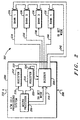
- FIG. 1 shows a prior art ATM cell processing system 100 which is coupled to connection memory 102 via chip select logic 104.
- the ATM cell processing system 100 comprises a micro processor 106 which controls the establishment of virtual connections via input lines 108 and output lines 110 which are coupled to the ATM cell processing system 100.
- the processor 106 detects various events while processing the cell flow of the virtual connections, such as running counts or other information required for billing purposes. Since there is a very high number of virtual connections which use a single physical link, the event indications detected by the processor 106 and the running counts have to be stored and maintained in the connection memory 102 which is organized as a random access memory (RAM).
- the processor 106 uses the connection memory 102 as its private memory. Since one single physical memory component does not have enough storage capacity for all the information which is to be stored by the processor 106, the connection memory 102 is split up into four memory banks 110, 112, 114 and 116.
- the memory banks 110-116 are connected via the address bus 118 to the micro processor 106.
- the chip select logic 104 is also connected to the address bus 118.
- the data bus which is needed for data transmittals from the micro processor 106 to the connection memory 102 and vice versa is not shown in the drawing for simplicity.
- the chip select logic 104 is coupled to the individual memory banks 110, 112, 114 and 116 via the bank select lines 120, 122, 124 and 126, respectively.
- the micro processor 106 When the micro processor 106 wants to access the connection memory 102, it issues a 20 bit wide address on the address bus 118.
- the bit positions 0-17 on the address bus 118 directly serve to access a specific storage location in one of the memory banks 110-116. All memory banks 110-116 receive the same address via the address bus 118.
- the two most significant bits, i.e. bit positions 18 and 19 of the address bus 118 are used in the chip select logic 104 to select one of the memory banks 110-116 which corresponds to the address of the access request of the micro processor 106 considered here.
- the 20 bit wide address space which can be accessed by the micro processor 106 is divided into four sections having the same size.
- Each section of the address space belongs to one of the memory banks 110-116.
- each section of the memory space has its own memory bank. If the two most significant bit positions 18 and 19 are logically "11" that means that the memory bank 110 which holds the upper portion of the memory space is to be accessed.
- the chip select logic 104 raises the bank select line 120 to enable the memory bank 110.
- the other bank select lines 122, 124 and 126 remain logically low so that the corresponding memory banks 112, 114 and 116 remain disabled.
- the address which is present on the address bus 118 is ignored by the disabled memory banks 112, 114 and 116 whereas the bit positions 0-17 of the address which is present on the address bus 118 are used in the memory bank 110 to access a specific memory location for read and/or write purposes.
- other sections of the memory space are addressed by the micro processor 106 other memory banks are selected to perform access operations.
- Such access operations can only be carried out when there is a "hole” in the cell flow.
- Such holes in the cell flow are provided periodically in the ATM cell processing system 100. This is accomplished by processing the ATM cells within the ATM cell processing system 100 at a rate slightly above the transmission rate of the physical input and output lines 108 and 110.
- the invention is aimed to provide an improved ATM cell processing system and an improved method for accessing a connection memory of such a system.
- the invention allows to more efficiently utilize the holes in the cell flow for maintenance purposes since the time required for an access operation to the connection memory from the micro processor is decreased.
- the invention is advantageous in that it allows to couple a connection memory to an ATM cell processing system without any glue logic. Since all the decoding to access the memory banks is done internal the ATM cell processing system, a flexible interface is provided which minimizes the restrictions and requirements for the external memory components used to realize the memory banks. Hence, it is possible to utilize a wide range of relatively inexpensive memory devices for the memory banks.
- the invention allows to minimize access times to the connection memory. This is due to the fact that no more glue logic is required and therefore the control and address signal lines are shorter and less loaded. There is no more need to buffer the signal lines to drive the load. Also the delay due to bank decoding in the external chip logic of the prior art is minimized since the decoding is done more efficiently within the boundary of the ATM cell processing system and can even be implemented on the same chip as the micro processor of the system. Performing the bank select decoding internally eliminates the uncertainty of the decoding delay from the interface design.
- the address space comprises two sets of bit positions: one for the purposes of generating a bank select signal and the other for addressing a memory location in one of the memory banks.
- a pointer can be used to separate the two sets of bit positions for the decoding of the address to generate the bank select signal and to address a memory location.
- the set of bit positions which serves to generate the bank select signal preferably occupies the most significant bit positions of the address.
- each memory bank serves to store a specific bit slice of a data word. If more than one bank is present it is also possible to realize each of the banks by a plurality of memory components each of which storing a bit slice.
- FIG. 2 shows ATM cell processing system 200 and connection memory 202.
- the ATM cell processing system 200 comprises micro processor 206, decoder 204 as well as the registers 212 and 214.
- the ATM cell processing system 200 has input lines 208 and output lines 210 which serve to establish physical connections. Via each physical connection a very high number of virtual logical connections are established under the control of the micro processor 206.
- the processing in the ATM cell processing system 200 is done by the micro processor 206 at a rate which is slightly above the physical transmission rate on the input and output lines 208 and 210 so that at regular intervals "holes" are provided in the cell flow. The time intervals in which such holes are present, are used for maintenance purposes which require access to the connection memory 202.
- the micro processor 206 is coupled to the decoder 204 via address bus 216.
- the address bus is 20 bit wide.
- the micro processor 206 is coupled via lines 218 and 220 to the registers 212 and 214, respectively.
- the registers 212 and 214 are coupled via lines 222 and 224, respectively, to the decoder 204.
- the connection memory 202 has four memory banks 226, 228, 230 and 232.
- the connection memory 202 is equivalent to the connection memory 102 shown in FIG. 1.
- the memory banks 226-232 are connected to bank select lines 234, 236, 238 and 240, respectively.
- the other sides of the bank select lines 234-240 are connected to the decoder 204.
- the address input of each of the memory banks 226-232 is connected to the address bus 242 which is also connected to the decoder 204.
- the register 212 serves as a storage means for storage of data indicative of the number of memory banks which in the example considered here is four.
- the register 214 serves as another storage means for storage of a pointer to a first set of bit positions which serve as a basis to generate bank select signals or, alternatively, for indicating the most significant bit position (MSB) in an address.
- MSB most significant bit position
- the micro processor 206 When the ATM cell processing system 200 is switched on the registers 212 and 214 are initialized by the micro processor 206.
- the micro processor 206 writes the number of memory banks which are coupled to the ATM cell processing system 200 to the register 212 via the signal line 218.
- the micro processor 206 also writes a pointer to the register 214 via the signal line 220.
- the pointer points to the first set of bit positions in an address of an access request of the micro processor 206. This set of bit positions serves as a basis to generate the bank select signal to select one of the memory banks 226 to 232 via one of the bank select lines 234-240, respectively.
- the pointer stored in the register 214 indicates which of the bit positions of an address carries the bank select information. If by definition, this set of bit positions is always placed in a coherent row in the address, one pointer stored in the register 214 is enough to identify this set of bit positions.
- the register 214 stores a pointer for each bit position belonging to the set.
- the register 214 can store 2 pointers which point to the bit positions B17 and B9, respectively.
- the decoder 204 understands this information to indicate that the bit positions B17 and B9 carry the bank select information.
- the information stored in the register 212 is redundant, since each bit position belonging to the set of bit positions carrying the bank select information has its own pointer stored in the register 214.
- the register 214 is adapted to store a plurality of pointers.
- the micro processor 206 can store information in the register 214 to indicate which of the bit positions B0-B19 is most significant. In some cases the whole address space of 20 bits is not required. In such a case the most significant bit position can be one of the lesser significant bit positions in the 20 bit wide address word. For example if the micro processor 206 stores a pointer to bit position B18 in the register 214, this means that the bit position B18 is defined to be the most significant bit position and that the bit position B19 is "don't care".
- bit position B0-B18 is utilized as a physical address for a memory location in the connection memory 202. If the number of memory banks is two, one bit is required for the bank select. This is the most significant bit B18. Likewise, if three or four memory banks are present, two bit positions are required to encode the bank select information. This information is carried by the bit positions B18 and B17. The further bit positions B16-B0 serve as a physical address for addressing of a specific memory location in the selected memory bank.
- the preferred embodiment shown in FIG. 3 differs from FIG. 2 in that only one logical memory bank 302 is present.
- the logical memory bank 302 is realized by the physical memory banks 303 to 310 each of which is a separate memory chip.
- Each of the physical memory banks 303-310 stores a bit slice of three bits of a 24 bit wide data word. As a consequence all 20 bits of the corresponding address word are necessary for each individual memory bank to address the appropriate bit slice.
- all memory banks 303-310 are connected to the 20 bit wide address bus 342.
- the memory banks 303-310 are coupled to the decoder 204 via their respective bank select lines 334-341. Since there is only one logical memory bank all bank select lines 334-341 are logically equivalent and receive the same select signal.
- the processor 206 stores "1" in the register 212 via the line 218 to indicate that only one logical memory bank is present. In this case the information stored in the register 214 is "don't care" since no bank decoding is required. If the micro processor 206 wants to access the connection memory 302 it issues an address word of 20 bits which is passed through the decoder via the address bus 342 to each of the memory banks 303 to 310. Since the number stored in the register 212 is "1", this indicates to the decoder that there is only one logical memory bank so that a bank select signal is outputted by the decoder 204 and transmitted via all bank select lines 334-341 to the corresponding memory banks 303-310.
- connection memory 302 The presence of a plurality of bank select lines for one logical memory bank has the advantage that the load of the lines is split between different drivers which are incorporated in the decoder 204 so that the access time to the connection memory 302 is further decreased.
- the ATM cell processing system 200 of the FIG. 2 and 3 can be connected to different arrangements of connection memories just by programming the registers 212 and 214. Since a well defined interface is provided a wide variety of different physical memory components can be used to realize a connection memory.
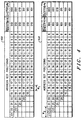
- FIG. 4 shows two examples for the programming of the registers 212 and 214.
- the address bit positions 23 to 8 are indicated.
- the address bit positions 7 to 0 are not shown for simplicity.
- the maximum width of an address word is 24 bits.
- the address bus between micro processor and decoder has to be 24 bits wide if the full address range is to be used.
- the table 400 refers to a preferred embodiment where two logical memory banks are present.
- the register 212 carries the binary information "010" which is the number of logical memory banks.
- the register 214 stores a pointer to the most significant bit in an address word. If the pointer stored in register 214 is "000” it points to the bit position B23. Likewise, if the pointer is "001” it points to the lesser significant bit position B22 so that the bit position B23 becomes “don't care”. Alternatively, if the register 214 has one of the pointers "010", “011”, "100” or "101" the corresponding most significant bit positions are B21, B20, B19 and B18.
- a window having the length of one bit position is defined which covers the set of bit positions which carry the bank select information.
- this set only contains one bit position which is the most significant bit position in the address word as defined by the pointer of register 214.
- This sliding window is denoted W 1 in the table 400.
- the table 410 of FIG. 4 shows the programming of the registers 212 and 214 for the case of four logical memory banks .
- the register 212 carries the binary information "100" and the register 214 can be programmed in the same way as illustrated in table 400. Since in the example shown in table 410 there are four logical memory banks instead of two logical memory banks. Two bit positions are required to carry the bank select information. Hence the sliding window has to carry a set of two bit positions. This sliding window is denoted W 2 in table 410.
- bit position B23 is the most significant bit position.
- the decoder considers this bit position B23 and the following bit position B22 to constitute the set of bit positions which carry the bank select information.
- the pointer stored in register 214 is "001”, “010”, “011”, “100” or "101” this corresponds to the set of bit positions B22, B21; B21, B20; B20, B19; B19, B18; and B18, B17.
- step 500 the micro processor 206 generates an address which is outputted via the address bus 216.
- the decoder 204 looks up the registers 212 and 214 in step 502. The information stored in the registers 212 and 214 determines first set of bit positions which carries the bank select information. These bit positions are covered by the sliding window W as shown in FIG. 4.
- the first set of bit positions is decoded by the decoder 204 in step 504.
- the second set of bit positions which carries the information to address a specific memory location in one of the physical memory banks of the connection memory 202 is also decoded in step 506 by the decoder 204.
- step 508 a bank select signal is generated and the appropriate bank select line or the appropriate bank select lines are driven correspondingly.
- the physical address to access a specific memory location is outputted in step 510.
- the micro processor 206 can read and/or write data to the required memory location.
Landscapes
- Engineering & Computer Science (AREA)
- Computer Networks & Wireless Communication (AREA)
- Data Exchanges In Wide-Area Networks (AREA)
Priority Applications (2)
| Application Number | Priority Date | Filing Date | Title |
|---|---|---|---|
| DE1996634295 DE69634295T2 (de) | 1996-06-19 | 1996-06-19 | ATM-Zellenverarbeitungssystem und Methode zum Zugriff auf einen Verbindungsspeicher |
| EP19960109860 EP0814630B1 (de) | 1996-06-19 | 1996-06-19 | ATM-Zellenverarbeitungssystem und Methode zum Zugriff auf einen Verbindungsspeicher |
Applications Claiming Priority (1)
| Application Number | Priority Date | Filing Date | Title |
|---|---|---|---|
| EP19960109860 EP0814630B1 (de) | 1996-06-19 | 1996-06-19 | ATM-Zellenverarbeitungssystem und Methode zum Zugriff auf einen Verbindungsspeicher |
Publications (2)
| Publication Number | Publication Date |
|---|---|
| EP0814630A1 true EP0814630A1 (de) | 1997-12-29 |
| EP0814630B1 EP0814630B1 (de) | 2005-02-02 |
Family
ID=8222906
Family Applications (1)
| Application Number | Title | Priority Date | Filing Date |
|---|---|---|---|
| EP19960109860 Expired - Lifetime EP0814630B1 (de) | 1996-06-19 | 1996-06-19 | ATM-Zellenverarbeitungssystem und Methode zum Zugriff auf einen Verbindungsspeicher |
Country Status (2)
| Country | Link |
|---|---|
| EP (1) | EP0814630B1 (de) |
| DE (1) | DE69634295T2 (de) |
Citations (2)
| Publication number | Priority date | Publication date | Assignee | Title |
|---|---|---|---|---|
| EP0320772A2 (de) * | 1987-12-18 | 1989-06-21 | Alcatel SEL Aktiengesellschaft | Verfahren zur hybriden Paketvermittlung und Einrichtungen hierzu |
| US5189666A (en) * | 1990-01-25 | 1993-02-23 | Nec Corporation | Bit-slice asynchronous transfer mode switching system |
-
1996
- 1996-06-19 EP EP19960109860 patent/EP0814630B1/de not_active Expired - Lifetime
- 1996-06-19 DE DE1996634295 patent/DE69634295T2/de not_active Expired - Fee Related
Patent Citations (2)
| Publication number | Priority date | Publication date | Assignee | Title |
|---|---|---|---|---|
| EP0320772A2 (de) * | 1987-12-18 | 1989-06-21 | Alcatel SEL Aktiengesellschaft | Verfahren zur hybriden Paketvermittlung und Einrichtungen hierzu |
| US5189666A (en) * | 1990-01-25 | 1993-02-23 | Nec Corporation | Bit-slice asynchronous transfer mode switching system |
Non-Patent Citations (2)
| Title |
|---|
| OECHSLIN P ET AL: "ALI: A VERSATILE INTERFACE CHIP FOR ATM SYSTEMS", COMMUNICATION FOR GLOBAL USERS, ORLANDO, DEC. 6 - 9, 1992, vol. 3 OF 3, 6 December 1992 (1992-12-06), INSTITUTE OF ELECTRICAL AND ELECTRONICS ENGINEERS, pages 1282 - 1287, XP000390422 * |
| T. SHANLEY: "The IBM PS/2 From the Inside Out", December 1990, ADDISON-WESLEY, 12.1990, XP002023813, 19406 * |
Also Published As
| Publication number | Publication date |
|---|---|
| DE69634295D1 (de) | 2005-03-10 |
| EP0814630B1 (de) | 2005-02-02 |
| DE69634295T2 (de) | 2005-06-09 |
Similar Documents
| Publication | Publication Date | Title |
|---|---|---|
| EP1192753B1 (de) | Verfahren und vorrichtung zur paketvermittlung mittels eines geteilten pufferspeichers | |
| EP1237337B1 (de) | Effizienter Optimierungsalgorithmus für Speichergebrauch in Netzwerkanwendungen | |
| US5261059A (en) | Crossbar interface for data communication network | |
| US5535197A (en) | Shared buffer switching module | |
| US5787255A (en) | Internetworking device with enhanced protocol translation circuit | |
| US7782849B2 (en) | Data switch and switch fabric | |
| US5657289A (en) | Expandable data width SAM for a multiport RAM | |
| US20050265357A1 (en) | Memory caching | |
| US20070274303A1 (en) | Buffer management method based on a bitmap table | |
| US5875173A (en) | Communication control device and method for use in an ATM system operable in an ABR mode | |
| WO1995015526A1 (en) | Method and system for managing memory in a high speed network | |
| US6728256B1 (en) | Shared buffer control device | |
| US7506081B2 (en) | System and method of maintaining high bandwidth requirement of a data pipe from low bandwidth memories | |
| EP0357618A1 (de) | Vermittlungssystem. | |
| EP0858716B1 (de) | Verbesserungen in oder sich beziehend auf einer atm-vermittlungsstelle | |
| EP0685795A1 (de) | Speicherabbildungseinrichtung für ein Signalverarbeitungssystem | |
| EP0814630B1 (de) | ATM-Zellenverarbeitungssystem und Methode zum Zugriff auf einen Verbindungsspeicher | |
| US6314489B1 (en) | Methods and systems for storing cell data using a bank of cell buffers | |
| US20020066000A1 (en) | Transporting data transmission units of different sizes using segments of fixed sizes | |
| EP0503560B1 (de) | Vermittlungseinheit zwischen den Eingängen und Ausgängen | |
| US5815499A (en) | ATM switch address generating circuit | |
| EP0718997A2 (de) | Digitaler Datenkonzentrator | |
| EP0446335B1 (de) | Pakete-/schnelle-pakete-vermittlung für sprache und daten | |
| EP1585024B1 (de) | Ein verbesserter on-chip Speicher zur Speicherung von variablen Datenbits | |
| US6871256B2 (en) | Method and arrangement in a stack having a memory segmented into data groups having a plurality of elements |
Legal Events
| Date | Code | Title | Description |
|---|---|---|---|
| PUAI | Public reference made under article 153(3) epc to a published international application that has entered the european phase |
Free format text: ORIGINAL CODE: 0009012 |
|
| AK | Designated contracting states |
Kind code of ref document: A1 Designated state(s): DE FR GB |
|
| 17P | Request for examination filed |
Effective date: 19980629 |
|
| 17Q | First examination report despatched |
Effective date: 20030623 |
|
| GRAP | Despatch of communication of intention to grant a patent |
Free format text: ORIGINAL CODE: EPIDOSNIGR1 |
|
| GRAS | Grant fee paid |
Free format text: ORIGINAL CODE: EPIDOSNIGR3 |
|
| RAP1 | Party data changed (applicant data changed or rights of an application transferred) |
Owner name: FREESCALE SEMICONDUCTOR, INC. |
|
| GRAA | (expected) grant |
Free format text: ORIGINAL CODE: 0009210 |
|
| AK | Designated contracting states |
Kind code of ref document: B1 Designated state(s): DE FR GB |
|
| REG | Reference to a national code |
Ref country code: GB Ref legal event code: FG4D |
|
| REF | Corresponds to: |
Ref document number: 69634295 Country of ref document: DE Date of ref document: 20050310 Kind code of ref document: P |
|
| PLBE | No opposition filed within time limit |
Free format text: ORIGINAL CODE: 0009261 |
|
| STAA | Information on the status of an ep patent application or granted ep patent |
Free format text: STATUS: NO OPPOSITION FILED WITHIN TIME LIMIT |
|
| ET | Fr: translation filed | ||
| 26N | No opposition filed |
Effective date: 20051103 |
|
| PGFP | Annual fee paid to national office [announced via postgrant information from national office to epo] |
Ref country code: DE Payment date: 20070629 Year of fee payment: 12 |
|
| PGFP | Annual fee paid to national office [announced via postgrant information from national office to epo] |
Ref country code: GB Payment date: 20070511 Year of fee payment: 12 |
|
| PGFP | Annual fee paid to national office [announced via postgrant information from national office to epo] |
Ref country code: FR Payment date: 20070605 Year of fee payment: 12 |
|
| GBPC | Gb: european patent ceased through non-payment of renewal fee |
Effective date: 20080619 |
|
| REG | Reference to a national code |
Ref country code: FR Ref legal event code: ST Effective date: 20090228 |
|
| PG25 | Lapsed in a contracting state [announced via postgrant information from national office to epo] |
Ref country code: DE Free format text: LAPSE BECAUSE OF NON-PAYMENT OF DUE FEES Effective date: 20090101 |
|
| PG25 | Lapsed in a contracting state [announced via postgrant information from national office to epo] |
Ref country code: GB Free format text: LAPSE BECAUSE OF NON-PAYMENT OF DUE FEES Effective date: 20080619 |
|
| PG25 | Lapsed in a contracting state [announced via postgrant information from national office to epo] |
Ref country code: FR Free format text: LAPSE BECAUSE OF NON-PAYMENT OF DUE FEES Effective date: 20080630 |