EP0814341A2 - Circuit for establishing an output signal corresponding to the amplitude of an input signal - Google Patents
Circuit for establishing an output signal corresponding to the amplitude of an input signal Download PDFInfo
- Publication number
- EP0814341A2 EP0814341A2 EP97109102A EP97109102A EP0814341A2 EP 0814341 A2 EP0814341 A2 EP 0814341A2 EP 97109102 A EP97109102 A EP 97109102A EP 97109102 A EP97109102 A EP 97109102A EP 0814341 A2 EP0814341 A2 EP 0814341A2
- Authority
- EP
- European Patent Office
- Prior art keywords
- summation
- output
- amplifier
- signal
- current
- Prior art date
- Legal status (The legal status is an assumption and is not a legal conclusion. Google has not performed a legal analysis and makes no representation as to the accuracy of the status listed.)
- Withdrawn
Links
Images

Classifications
-
- G—PHYSICS
- G01—MEASURING; TESTING
- G01R—MEASURING ELECTRIC VARIABLES; MEASURING MAGNETIC VARIABLES
- G01R19/00—Arrangements for measuring currents or voltages or for indicating presence or sign thereof
- G01R19/04—Measuring peak values or amplitude or envelope of ac or of pulses
Definitions
- the invention relates to a circuit arrangement for forming an output signal corresponding to the amplitude of an input signal.
- Such a circuit arrangement is from Tietze, Schenk: Semiconductor circuit technology ", Springer-Verlag, 1978, pages 662-663.
- the circuit arrangement described there has a first voltage follower to which the input signal is supplied, a second voltage follower which supplies the output signal, a diode, a series resistor, a capacitor and The input of the second voltage follower is connected to the output of the first voltage follower via the diode and the series resistor connected in series therewith, and to ground via the capacitor and the switch connected in parallel.
- the switch is first opened.
- the capacitor is thus charged to a charge corresponding to the instantaneous value of the input signal as the amplitude of the input signal increases via the diode and the series resistor. If the amplitude of the input signal drops, however, the charge on the capacitor is retained, since the diode prevents the capacitor from being discharged via the first voltage follower and since the second voltage follower does not load the capacitor.
- the charge of the capacitor is accordingly a measure of the amplitude of the input signal, so that the second voltage follower delivers the output signal corresponding to the amplitude of the input signal as a measurement result.
- the capacitor can then be discharged for a new measurement via the switch.
- the main disadvantage of the circuit arrangement is that the capacitor is only delayed, i. H. asymptotic, to which the charge corresponding to the current value of the input signal is charged and that the measurement consequently becomes less precise with increasing frequency of the input signal.
- the cause of this delay is the voltage drop across the series resistor, which is connected between the first voltage follower and the capacitor in order to reduce the tendency to oscillate in the circuit arrangement.
- no continuous measurements can be carried out with the circuit arrangement, since the capacitor must be discharged via the switch for each measurement. Interference caused by switching operations can cause measurement errors.
- the capacitor takes up considerable chip area when the circuit arrangement is integrated into an integrated circuit.
- the invention has for its object to provide an advantageous circuit arrangement according to the preamble of claim 1, which can be inexpensively integrated into an integrated circuit with little circuit complexity, which is operated without clocking, which provides accurate measurement results and which can be used in particular for measuring the amplitude of high-frequency input signals is.
- the amplifier stages of the circuit arrangement according to the invention are designed as temperature-compensated amplifiers, ie as amplifiers with amplification factors that are independent of the temperature of the amplifier stages, preferably the same. They are connected as an amplifier chain, ie they are connected in series one behind the other, an amplifier input of a downstream amplifier stage being connected to an amplifier output of the previous amplifier stage. Depending on the amplitude of the input signal, the amplifier stages can be overdriven, ie saturated. An amplifier stage is overdriven or saturated when a signal fed to its amplifier input exceeds a modulation limit of the amplifier stage, so that a distortion-free amplification is no longer possible.
- the amplifier stages each have a measurement output at which a measurement signal corresponding to the modulation of the respective amplifier stage is present.
- a summation unit connected to the measurement outputs of the amplifier stages generates, by summing the measurement signals, a sum signal which is present as an output signal at a summation output of the summation unit.
- the sum signal is essentially determined by the number of overdriven, ie saturated, amplifier stages and is consequently a measure of the amplitude of the input signal. For amplifier stages with the same amplification factors, it is roughly proportional to the logarithm of the amplitude of the input signal.
- the circuit arrangement is suitable for carrying out continuous measurements. Due to the lack of feedback in the amplifier chain, it has a low tendency to oscillate, so that it is also suitable for measuring the amplitude of high-frequency input signals.
- the amplifier stages preferably each have two bipolar amplifier transistors in a differential amplifier circuit, each having an emitter current source connected to the emitter connections of the amplifier transistors, which supplies a cross current proportional to the temperature of the amplifier stages, and each having an output current source which can be controlled by the emitter connections of the amplifier transistors and which is advantageously designed as a bipolar output transistor and delivers a measuring current as a measuring signal at the measuring output.
- the amplifier inputs and the amplifier outputs of the amplifier stages are designed as differential input connections or as differential output connections, the base connections or the collector connections of the amplifier transistors of an amplifier stage each being connected to one of the differential input connections or output connections of this amplifier stage.
- the summation unit generates the summation signal from the measurement currents, preferably by summation and subsequent low-pass filtering, which, for example, is the summation current from a summation output of the Summation unit can be decoupled for further processing or evaluation.
- the circuit arrangement has a large dynamic range, i. H. Both very small amplitudes and large amplitudes can be measured, so that it is ideally suited for measuring the field strength of a radio signal.
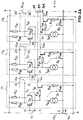
- the circuit arrangement comprises an amplifier chain with the amplifier stages V 1 ... V n connected in series and the summation unit S.
- the amplifier stages V 1 ... V n are all designed as temperature-compensated differential amplifiers, each with the same and temperature-independent gain factors. They each have two differential input connections 10 and 11 or 20 and 21 or 30 and 31 or n0 and n1 as amplifier inputs, each have two differential output connections 12 and 13 or 22 and 23 or 32 and 33 or n3 and n4 as Amplifier output and one measuring output 14 or 24 or 34 or n4.
- the input connections 20, 21 or 30, 31 or n0, n1 of the amplifier stages V 2 , V 3 ... V n following in the amplifier chain of the first amplifier stage V 1 are each connected to one of the output connections 12, 13 or 22, 23 or 32, 33 of the upstream amplifier stage V 1 , V 2 , V 3 , ... connected.
- the input signal U E is fed to the input connections 10 and 11 of the first amplifier stage V 1 as an input voltage. This is achieved by the amplifier stages V 1 ... V n , provided the amplitude of the input signal U E is so small that none of the amplifier stages V 1 ... V n is overdriven, ie saturated, by the product of the gain factors of all amplifier stages V 1 ... V n reinforced. As the amplitude of the input signal U E increases , starting with the last amplifier stage V n - always overdriven several of the amplifier stages V 1 ... V n . The output voltage U Vn present at the output connections n2, n3 of the last amplifier stage V n is then limited and thus distorted.
- V n deliver at their measuring outputs 14 or 24 or 34 or n4, which are all connected to the summation unit S, a measuring current I M1 or ... I Mn as the measuring signal, which the Control of the respective amplifier stage corresponds to V 1 ... V n , ie it indicates how strongly the respective amplifier stage V 1 ... V n is overdriven or saturated.
- the measuring currents I M1 ... I Mn are fed to the summation unit S, summed by them and low-pass filtered for averaging.
- the summation unit S then supplies a summation current as the sum signal I S , which is greater the more of the amplifier stages V 1 ... V n are saturated and which is consequently a measure of the amplitude of the input signal U E.
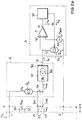
- FIG. 2a which shows a circuit arrangement with three amplifier stages V 1 , V 2 , V 3 as an exemplary embodiment of the amplifier chain from FIG. 1, the amplifier stages V 1 , V 2 , V 3 are differential amplifiers, each with two bipolar amplifier transistors T 10 and T 11 or T 20 and T 21 or T 30 and T 31 , each having an emitter current source Q 1 or Q 2 or Q 3 , in each case a controllable output current source designed as an output transistor T 12 or T 23 or T 32 and in each case two collector resistors R 10 and R 11 or R 20 and R 21 or R 30 and R 31 are formed.
- the base connections of the amplifier transistors T 10 and T 11 or T 20 and T 21 or T 30 and T 31 are each connected to one of the input connections 10 and 11 or 20 and 21 or 30 and 31, the collector connections of the amplifier transistors T 10 and T 11 or T 20 and T 21 or T 30 and T 31 are each connected to one of the output connections 12 and 13 or 22 and 23 or 32 and 33, the output connections 12 or 13 or 22 or 23 or 32 or 33 via the collector resistors R 10 or R 11 or R 20 or R 21 or R 30 or R 31 connected to the first supply connection 1, to which the supply voltage U CC is applied, the emitter connections of the Amplifier transistors T 10 and T 11 or T 20 and T 21 or T 30 and T 31 with the base connection of the output transistor T 12 or T 23 or T 32 and via the emitter current source Q 1 or Q 2 or Q 3 with the second supply connection 2, to which a reference potential is connected, the collector connections of the off gang transistors T 12 or T 23 or T 32 each connected to the measuring output 14 or 24 or 34 and the emitter
- the emitter connections of the Vetttärker transistors T 10 and T 11 or T 20 and T 21 or T 30 and T 31 are advantageously via the base resistors R 12 or R 22 or R 32 to the base connections of the output transistors T 12 or T 23 or T 32 and the emitter connections of the output transistors T 12 , T 22 , T 32 are each connected to the third supply connection 3 via one of the emitter resistors R 13, R 14 and R 15 .
- the emitter current sources Q 1 , Q 2 , Q 3 are each designed as a bipolar transistor or as a field effect transistor, for example as a MOS transistor, which are controlled in such a way that they are proportional to and proportional to the temperature of the amplifier stages V 1 , V 2 , V 3 supply a cross-current I Q1 or I Q2 or I Q3 which is inversely proportional to a given reference resistance .
- the amplification factors of the amplifier stages V 1 , V 2 , V 3 since they are known to be proportional to the respective cross current I Q1 or I Q2 or I Q3 , are proportional to the respective collector resistances R 10 , R 11 or R 20 , R 21 or R 30 , R 31 and inversely proportional to the temperature of the amplifier transistors T 10 , T 11 or T 21 , T 22 or T 31 , T 32 and thus inversely proportional to the temperature of the amplifier stages V 1 or V 2 or V 3 are independent of temperature.
- the measuring currents I M1 or I M2 or I M3 flowing through the measuring outputs 14 or 24 or 34 are determined by the emitter voltages U VE1 or U VE2 or U VE2 of the respective amplifier transistors T 10 , T 11 or T 20 , T 21 or T 30 , T 31 controlled.
- This emitter voltages U VE1 or U VE2 or U VE2 each comprise a DC component and a respective of the alternating component of the respective amplifier stage V 1 and V 2 and V 3 applied voltage U E and U V1, U V2 by rectifying formed rectified portion.
- the measuring currents I M1 or I M2 or I M3 are therefore each composed of a quiescent component and a modulation component.
- the quiescent components are those components of the measuring currents I M1 or I M2 or I M3 that flow when the amplitude of the input signal U E is 0 V.
- the modulation components depend on the modulation of the respective amplifier stage V 1 or V 2 or V 3 , ie on the amplitude of the voltage U E or U V1 or U V2 supplied to the respective amplifier stage V 1 or V 2 or V 3 dependent and they are each at a maximum value for overdriven amplifier stages V 1 , V 2 , V 3 limited.
- the voltages U V1 , U V2 , U V3 supplied by the amplifier stages V 1 , V 2 , V 3 are also temperature-independent, so that with the same amplitude of the input signal U E always the same number of amplifier stages V 1 , V 2 , V 3 are overdriven.
- the maximum value of the measuring currents I M1 , I M2 , I M3 is approximately linearly dependent on the temperature.
- the I Q1, I Q2 and I Q3 dependent on the cross-currents to the emitter terminals of the amplifier transistors T 10, T 11 and T 20, T 21 and T 30, T 31 pending emitter voltages U VE1 and U VE2 or U VE3 , through which the output transistors T 12 or T 22 or T 32 are controlled.
- FIG. 2b which shows an exemplary embodiment of the summation unit S from FIG. 1 and an evaluation unit A as an exemplary embodiment of a circuit arrangement for evaluating the sum signal I S
- the summation unit S has one with the measurement outputs 14, 24, 34 of the amplifier stages V 1 and V 2 or V 3 connected summation node 50, a quiescent current source Q 0 , via which the summation node 50 is connected to the first supply connection 1, and a low-pass filter TP, via which the summation node 50 is connected to the summation output 51 of the summation unit S.
- the output 52 of the low-pass filter TP is designed as a current output, ie the low-pass filter TP has an output current source Q S for decoupling the summation current I S.
- the evaluation unit A comprises the controllable comparison current source Q V , the comparison unit K and the control unit ST.
- the comparison current source Q V is connected to the summation output 51 and to the input 60 of the comparison unit K.
- the comparison current I V of the comparison current source Q V can be reversed by a digital control signal S D supplied by the control unit ST between different reference resistors proportional to the temperature of the amplifier stages V 1 , V 2 , V 3 and to the predetermined reference resistance proportional current values can be switched.
- the comparison current source Q V accordingly acts as a digital-to-analog converter, which generates an analog current - the comparison current I V - with the same temperature coefficient as the summation current I S from the digital control signal S D.
- To control the comparison current I V it has a control input 62, which is connected via the control unit ST to the output 61 of the comparison stage K and to which the digital control signal S D is supplied.
- the comparison current source Q V of the evaluation unit A and the output current source Q S of the low-pass filter TP are designed as bipolar transistors or as field-effect transistors, for example as MOS transistors.
- the measuring currents I M1 , I M2 , I M3 are summed at the summing node 50, their quiescent components being compensated for by a quiescent current I 0 supplied by the quiescent current source Q 0 .
- the low-pass filter TP is therefore only supplied with a sum measurement current I MS composed of the modulation components of the measurement currents I M1 , I M2 , I M3 , which has frequency components originating from the input signal U E.
- the low-pass filter TP generates the summation current I S from the total measurement current I MS by suppressing the frequency components originating from the input signal U E , which due to its dependence on the measurement currents I M1 , I M2 , I M3 is proportional to the temperature of the amplifier stages V 1 , V 2 , V 3 is.
- a temperature-independent voltage U S is set which, depending on whether the summation current I S is greater or less than the comparison current I V, is greater or less than one Threshold voltage U SCH is.
- a temperature-independent evaluation signal U A is therefore present at the output 61 of the comparison stage K, which corresponds to the sign of the difference between the comparison current I V and the summation current I S.
- the comparison current source Q V is controlled by the control unit ST in such a way that the comparison current I V tracks the summation current I S.
- the digital control signal S D is varied, the control unit ST using the evaluation signal U A recognizing in which direction the variation of the digital control signal S D must take place. Because of the temperature independence of the evaluation signal U A , the digital control signal S D is also temperature independent, so that the amplitude of the input signal U E corresponds to the digital control signal S D , ie can be assigned a value corresponding to the digital control signal S D.
Abstract
Description
Die Erfindung betrifft eine Schaltungsanordnung zur Bildung eines der Amplitude eines Eingangssignals entsprechenden Ausgangssignals.The invention relates to a circuit arrangement for forming an output signal corresponding to the amplitude of an input signal.
Eine derartige Schaltungsanordnung ist aus Tietze, Schenk: ![]()
![]()
Zur Bildung des der Amplitude des Eingangssignals entsprechenden Ausgangssignals, d. h. zur Messung der Amplitude des Eingangssignals, wird zunächst der Schalter geöffnet. Der Kondensator wird somit bei steigender Amplitude des Eingangssignals über die Diode und den Vorwiderstand auf eine dem momentanen Wert des Eingangssignals entsprechende Ladung aufgeladen. Bei fallender Amplitude des Eingangssignals bleibt die Ladung des Kondensators hingegen erhalten, da die Diode eine Entladung des Kondensators über den ersten Spannungsfolger verhindert und da der zweite Spannungsfolger den Kondensator nicht belastet. Die Ladung des Kondensators ist demnach ein Maß der Amplitude des Eingangssignals, so daß der zweite Spannungsfolger als Meßergebnis das der Amplitude des Eingangssignals entsprechende Ausgangssignal liefert. Über den Schalter läßt sich der Kondensator anschließend für eine neue Messung entladen.In order to form the output signal corresponding to the amplitude of the input signal, ie to measure the amplitude of the input signal, the switch is first opened. The capacitor is thus charged to a charge corresponding to the instantaneous value of the input signal as the amplitude of the input signal increases via the diode and the series resistor. If the amplitude of the input signal drops, however, the charge on the capacitor is retained, since the diode prevents the capacitor from being discharged via the first voltage follower and since the second voltage follower does not load the capacitor. The charge of the capacitor is accordingly a measure of the amplitude of the input signal, so that the second voltage follower delivers the output signal corresponding to the amplitude of the input signal as a measurement result. The capacitor can then be discharged for a new measurement via the switch.
Der wesentliche Nachteil der Schaltungsanordnung besteht darin, daß der Kondensator nur verzögert, d. h. asymptotisch, auf die dem momentanen wert des Eingangssignals entsprechende Ladung aufgeladen wird und daß die Messung demzufolge mit zunehmender Frequenz des Eingangssignals ungenauer wird. Ursache dieser Verzögerung ist der Spannungsabfall am Vorwiderstand, welcher zur Reduzierung der Schwingungsneigung der Schaltungsanordnung zwischen den ersten Spannungsfolger und den Kondensator geschaltet ist. Des weiteren lassen sich mit der Schaltungsanordnung keine kontinuierlichen Messungen durchführen, da der Kondensator für jede Messung über den Schalter entladen werden muß. Durch Schaltvorgänge bedingte Störungen können dabei Meßfehler verursachen. Außerdem beansprucht der Kondensator bei der Integration der Schaltungsanordnung in einen integrierten Schaltkreis erhebliche Chipfläche.The main disadvantage of the circuit arrangement is that the capacitor is only delayed, i. H. asymptotic, to which the charge corresponding to the current value of the input signal is charged and that the measurement consequently becomes less precise with increasing frequency of the input signal. The cause of this delay is the voltage drop across the series resistor, which is connected between the first voltage follower and the capacitor in order to reduce the tendency to oscillate in the circuit arrangement. Furthermore, no continuous measurements can be carried out with the circuit arrangement, since the capacitor must be discharged via the switch for each measurement. Interference caused by switching operations can cause measurement errors. In addition, the capacitor takes up considerable chip area when the circuit arrangement is integrated into an integrated circuit.
Der Erfindung liegt die Aufgabe zugrunde, eine vorteilhafte Schaltungsanordnung gemäß dem Oberbegriff des Patentanspruchs 1 anzugeben, die mit geringem Schaltungsaufwand kostengünstig in einen integrierten Schaltkreis integrierbar ist, die ungetaktet betrieben wird, die genaue Meßergebnisse liefert und die insbesondere zur Messung der Amplitude von hochfrequenten Eingangssignalen einsetzbar ist.The invention has for its object to provide an advantageous circuit arrangement according to the preamble of
Die Aufgabe wird erfindungsgemäß durch die kennzeichnenden Merkmale des Patentanspruchs 1 gelöst. Vorteilhafte Ausgestaltungen und Weiterbildungen ergeben sich aus den Unteransprüchen.The object is achieved by the characterizing features of
Die Verstärkerstufen der erfindungsgemäßen Schaltungsanordnung sind als temperaturkompensierte Verstärker, d. h. als Verstärker mit von der Temperatur der Verstärkerstufen unabhängigen, vorzugsweise gleichen Verstärkungsfaktoren ausgebildet. Sie sind als Verstärkerkette beschaltet, d. h. sie sind in Reihe hintereinander geschaltet, wobei ein Verstärkereingang einer nachgeschalteten Verstärkerstufe mit einem Verstärkerausgang der vorherigen Verstärkerstufe verbunden ist. Die Verstärkerstufen können in Abhängigkeit der Amplitude des Eingangssignals übersteuert, d. h. gesättigt werden. Eine verstärkerstufe ist dabei dann übersteuert oder gesättigt, wenn ein ihrem Verstärkereingang zugeführtes Signal eine Aussteuergrenze der Verstärkerstufe überschreitet, so daß eine verzerrungsfreie Verstärkung nicht mehr möglich ist. Die Verstärkerstufen weisen jeweils einen Meßausgang auf, an dem ein der Aussteuerung der jeweiligen Verstärkerstufe entsprechendes Meßsignal ansteht. Eine mit den Meßausgängen der Verstärkerstufen verbundene Summationseinheit erzeugt durch Summation der Meßsignale ein Summensignal, das als Ausgangssignal an einem Summationsausgang der Summationseinheit ansteht. Das Summensignal wird im wesentlichen durch die Anzahl der übersteuerten, d. h. gesättigten, Verstärkerstufen bestimmt und ist demzufolge ein Maß der Amplitude des Eingangssignals. Es ist bei Verstärkerstufen mit jeweils gleichen Verstärkungsfaktoren in etwa proportional zum Logarithmus der Amplitude des Eingangssignals.The amplifier stages of the circuit arrangement according to the invention are designed as temperature-compensated amplifiers, ie as amplifiers with amplification factors that are independent of the temperature of the amplifier stages, preferably the same. They are connected as an amplifier chain, ie they are connected in series one behind the other, an amplifier input of a downstream amplifier stage being connected to an amplifier output of the previous amplifier stage. Depending on the amplitude of the input signal, the amplifier stages can be overdriven, ie saturated. An amplifier stage is overdriven or saturated when a signal fed to its amplifier input exceeds a modulation limit of the amplifier stage, so that a distortion-free amplification is no longer possible. The amplifier stages each have a measurement output at which a measurement signal corresponding to the modulation of the respective amplifier stage is present. A summation unit connected to the measurement outputs of the amplifier stages generates, by summing the measurement signals, a sum signal which is present as an output signal at a summation output of the summation unit. The sum signal is essentially determined by the number of overdriven, ie saturated, amplifier stages and is consequently a measure of the amplitude of the input signal. For amplifier stages with the same amplification factors, it is roughly proportional to the logarithm of the amplitude of the input signal.
Da die Verstärkerstufen temperaturkompensiert sind, sind ihre Verstärkungsfaktoren temperaturunabhängig, so daß bei gleicher Amplitude des Eingangssignal immer die gleiche Anzahl von Verstärkerstufen übersteuert sind. Die Schaltungsanordnung ist zur Durchführung von kontinuierlichen Messungen geeignet. Sie weist aufgrund fehlender Rückkopplung in der verstärkerkette eine geringe Schwingungsneigung auf, so daß sie sich auch zur Amplitudenmessung von hochfrequenten Eingangssignalen eignet.Since the amplifier stages are temperature-compensated, their amplification factors are temperature-independent, so that the same number of amplifier stages are always overdriven with the same amplitude of the input signal. The circuit arrangement is suitable for carrying out continuous measurements. Due to the lack of feedback in the amplifier chain, it has a low tendency to oscillate, so that it is also suitable for measuring the amplitude of high-frequency input signals.
Die Verstärkerstufen weisen vorzugsweise jeweils zwei bipolare Verstärkertransistoren in Differenzverstärkerschaltung, jeweils eine mit den Emitteranschlüssen der Verstärkertransistoren verbundene Emitterstromquelle, die einen zur Temperatur der Verstärkerstufen proportionalen Querstrom liefert, und jeweils eine durch die Emitteranschlüsse der Verstärkertransistoren steuerbare Ausgangsstromquelle auf, welche vorteilhafterweise als bipolarer Ausgangstransistor ausgebildet ist und am Meßausgang einen Meßstrom als Meßsignal liefert. Die Verstärkereingänge und die Verstärkerausgänge der Verstärkerstufen sind dabei als differentielle Eingangsanschlüsse bzw. als differentielle Ausgangsanschlüsse ausgebildet, wobei die Basisanschlüsse bzw. die Kollektoranschlüsse der Verstärkertransistoren einer Verstärkerstufe jeweils mit einem der differentiellen Eingangsanschlüsse bzw. Ausgangsanschlüsse dieser Verstärkerstufe verbunden sind.The amplifier stages preferably each have two bipolar amplifier transistors in a differential amplifier circuit, each having an emitter current source connected to the emitter connections of the amplifier transistors, which supplies a cross current proportional to the temperature of the amplifier stages, and each having an output current source which can be controlled by the emitter connections of the amplifier transistors and which is advantageously designed as a bipolar output transistor and delivers a measuring current as a measuring signal at the measuring output. The amplifier inputs and the amplifier outputs of the amplifier stages are designed as differential input connections or as differential output connections, the base connections or the collector connections of the amplifier transistors of an amplifier stage each being connected to one of the differential input connections or output connections of this amplifier stage.
Die Summationseinheit erzeugt aus den Meßströmen vorzugsweise durch Summation und anschließende Tiefpaßfilterung das Summensignal, welches beispielsweise als Summationsstrom aus einem Summationsausgang der Summationseinheit zur weiteren Verarbeitung oder Auswertung auskoppelbar ist.The summation unit generates the summation signal from the measurement currents, preferably by summation and subsequent low-pass filtering, which, for example, is the summation current from a summation output of the Summation unit can be decoupled for further processing or evaluation.
Die Schaltungsanordnung weist einen großen Dynamikbereich auf, d. h. es sind sowohl sehr geringe Amplituden als auch große Amplituden meßbar, so daß sie bestens zur Messung der Feldstärke eines Funksignals geeignet ist.The circuit arrangement has a large dynamic range, i. H. Both very small amplitudes and large amplitudes can be measured, so that it is ideally suited for measuring the field strength of a radio signal.
Die Erfindung wird im folgenden anhand der Figuren näher beschrieben. Es zeigen:
Figur 1- ein Prinzipschaltbild der erfindungsgemäßen Schaltungsanordnung und
- Figur 2a und 2b
- ein Ausführungsbeispiel der Schaltungsanordnung aus
Figur 1 mit einer Auswerteeinheit.
- Figure 1
- a schematic diagram of the circuit arrangement according to the invention and
- Figure 2a and 2b
- an embodiment of the circuit arrangement of Figure 1 with an evaluation unit.
Gemäß der Figur 1 umfaßt die Schaltungsanordnung eine Verstärkerkette mit den hintereinander in Reihe geschalteten Verstärkerstufen V1 ... Vn und die Summationseinheit S. Die Verstärkerstufen V1 ... Vn sind alle als temperaturkompensierte Differenzverstärker mit jeweils gleichen und temperaturunabhängigen Verstärkungsfaktoren ausgeführt. Sie weisen jeweils zwei differentielle Eingangsanschlüsse 10 und 11 bzw. 20 und 21 bzw. 30 und 31 bzw. n0 und n1 als Verstärkereingang, jeweils zwei differentielle Ausgangsanschlüsse 12 und 13 bzw. 22 und 23 bzw. 32 und 33 bzw. n3 und n4 als Verstärkerausgang und jeweils einen Meßausgang 14 bzw. 24 bzw. 34 bzw. n4 auf. Die Eingangsanschlüsse 20, 21 bzw. 30, 31 bzw. n0, n1 der in der Verstärkerkette der ersten Verstärkerstufe V1 folgenden Verstärkerstufen V2, V3 ... Vn sind dabei jeweils mit einem der Ausgangsanschlüsse 12, 13 bzw. 22, 23 bzw. 32, 33 der jeweils vorgeschalteten Verstärkerstufe V1, V2, V3, ... verbunden.According to FIG. 1, the circuit arrangement comprises an amplifier chain with the amplifier stages V 1 ... V n connected in series and the summation unit S. The amplifier stages V 1 ... V n are all designed as temperature-compensated differential amplifiers, each with the same and temperature-independent gain factors. They each have two
Das Eingangssignal UE wird den Eingangsanschlüssen 10 und 11 der ersten Verstärkerstufe V1 als Eingangsspannung zugeführt. Diese wird durch die Verstärkerstufen V1 ... Vn, sofern die Amplitude des Eingangssignal UE so klein ist, daß keine der Verstärkerstufen V1 ... Vn übersteuert, d. h. gesättigt wird, um das Produkt der verstärkungsfaktoren aller Verstärkerstufen V1 ... Vn verstärkt. Bei zunehmender Amplitude des Eingangssignals UE werden - beginnend mit der letzten Verstärkerstufe Vn - immer mehrere der Verstärkerstufen V1 ... Vn übersteuert. Die an den Ausgangsanschlüssen n2, n3 der letzten Verstärkerstufe Vn anstehende Ausgangsspannung UVn ist dann begrenzt und somit verzerrt. Die Verstärkerstufen V1 ... Vn liefern an ihren Meßausgängen 14 bzw. 24 bzw. 34 bzw. n4, welche alle mit der Summationseinheit S verbunden sind, jeweils einen Meßstrom IM1 bzw. ... IMn als Meßsignal, der der Aussteuerung der jeweiligen Verstärkerstufe V1 ... Vn entspricht, d. h. der anzeigt, wie stark die jeweilige Verstärkerstufe V1 ... Vn übersteuert oder gesättigt ist. Die Meßströme IM1 ... IMn werden der Summationseinheit S zugeführt, durch diese summiert und zur Mittelwertsbildung tiefpaßgefiltert. Die Summationseinheit S liefert dann einen Summationsstrom als Summensignal IS, der um so größer ist, je mehrere der Verstärkerstufen V1 ... Vn gesättigt sind und der demzufolge ein Maß der Amplitude des Eingangssignal UE ist.The input signal U E is fed to the
Gemäß Figur 2a, die eine Schaltungsanordnung mit drei Verstärkerstufen V1, V2, V3 als Ausführungsbeispiel der Verstärkerkette aus Figur 1 zeigt, sind die Verstärkerstufen V1, V2, V3 als Differenzverstärker mit jeweils zwei bipolaren Verstärkertransistoren T10 und T11 bzw. T20 und T21 bzw. T30 und T31, jeweils einer Emitterstromquelle Q1 bzw. Q2 bzw. Q3, jeweils einer als Ausgangstransistor T12 bzw. T23 bzw. T32 ausgeführten steuerbaren Ausgangsstromquelle und jeweils zwei Kollektorwiderständen R10 und R11 bzw. R20 und R21 bzw. R30 und R31 ausgebildet. Dabei sind die Basisanschlüsse der Verstärkertransistoren T10 und T11 bzw. T20 und T21 bzw. T30 und T31 mit jeweils einem der Eingangsanschlüsse 10 und 11 bzw. 20 und 21 bzw. 30 und 31 verbunden, die Kollektoranschlüsse der Verstärkertransistoren T10 und T11 bzw. T20 und T21 bzw. T30 und T31 mit jeweils einem der Ausgangsanschlüsse 12 und 13 bzw. 22 und 23 bzw. 32 und 33 verbunden, die Ausgangsanschlüsse 12 bzw. 13 bzw. 22 bzw. 23 bzw. 32 bzw. 33 über die Kollektorwiderstände R10 bzw. R11 bzw. R20 bzw. R21 bzw. R30 bzw. R31 mit dem ersten Versorgungsanschluß 1, an dem die Versorgungsspannung UCC anliegt, verbunden, die Emitteranschlüsse der Verstärkertransistoren T10 und T11 bzw. T20 und T21 bzw. T30 und T31 mit dem Basisanschluß des Ausgangstransistors T12 bzw. T23 bzw. T32 und über die Emitterstromquelle Q1 bzw. Q2 bzw. Q3 mit dem zweiten Versorgungsanschluß 2, an dem ein Bezugspotential anliegt verbunden, die Kollektoranschlüsse der Ausgangstransistoren T12 bzw. T23 bzw. T32 jeweils mit dem Meßausgang 14 bzw. 24 bzw. 34 verbunden und die Emitteranschlüsse der Ausgangstransistoren T12 bzw. T23 bzw. T32 jeweils mit dem dritten Versorgungsanschluß 3, an dem eine Gleichspannung UK zur Einstellung des Arbeitspunktes der Ausgangstransistoren T12, T22, T32 ansteht, verbunden. Hierbei sind die Emitteranschlüsse der Vetttärkertransistoren T10 und T11 bzw. T20 und T21 bzw. T30 und T31 vorteilhafterweise über die Basiswiderstände R12 bzw. R22 bzw. R32 an die Basisanschlüsse der Ausgangstransistoren T12 bzw. T23 bzw. T32 angeschlossen und die Emitteranschlüsse der Ausgangstransistoren T12, T22, T32 über jeweils einen der Emitterwiderstände R13 bzw. R14 bzw. R15 an den dritten Versorgungsanschluß 3 angeschlossen.According to FIG. 2a, which shows a circuit arrangement with three amplifier stages V 1 , V 2 , V 3 as an exemplary embodiment of the amplifier chain from FIG. 1, the amplifier stages V 1 , V 2 , V 3 are differential amplifiers, each with two bipolar amplifier transistors T 10 and T 11 or T 20 and T 21 or T 30 and T 31 , each having an emitter current source Q 1 or Q 2 or Q 3 , in each case a controllable output current source designed as an output transistor T 12 or T 23 or T 32 and in each case two collector resistors R 10 and R 11 or R 20 and R 21 or R 30 and R 31 are formed. The base connections of the amplifier transistors T 10 and T 11 or T 20 and T 21 or T 30 and T 31 are each connected to one of the
Die Emitterstromquellen Q1, Q2, Q3 sind jeweils als Bipolartransistor oder als Feldeffektransistor, beispielsweise als MOS-Transistor, ausgebildet, die derart angesteuert werden, daß sie jeweils einen zur Temperatur der Verstärkerstufen V1, V2, V3 proportionalen und zu einem vorgegebenen Referenzwiderstand umgekehrt proportionalen Querstrom IQ1 bzw. IQ2 bzw. IQ3 liefern. Folglich sind die Verstärkungsfaktoren der Verstärkerstufen V1, V2, V3, da sie bekanntlich proportional zum jeweiligen Querstrom IQ1 bzw. IQ2 bzw. IQ3, proportional zu den jeweiligen Kollektorwiderständen R10, R11 bzw. R20, R21 bzw. R30, R31 und umgekehrt proportional zur Temperatur der Verstärkertransistoren T10, T11 bzw. T21, T22 bzw. T31, T32 und somit umgekehrt proportional zur Temperatur der Verstärkerstufen V1 bzw. V2 bzw. V3 sind, temperaturunabhängig. Die durch die Meßausgänge 14 bzw. 24 bzw. 34 fließenden Meßströme IM1 bzw. IM2 bzw. IM3 werden durch die Emitterspannungen UVE1 bzw. UVE2 bzw. UVE2 der jeweiligen Verstärkertransistoren T10, T11 bzw. T20, T21 bzw. T30, T31 gesteuert. Diese Emitterspannungen UVE1 bzw. UVE2 bzw. UVE2 weisen jeweils einen Gleichanteil und jeweils einen aus dem wechselanteil der der jeweiligen Verstärkerstufe V1 bzw. V2 bzw. V3 zugeführten Spannung UE bzw. UV1 bzw. UV2 durch Gleichrichtung gebildeten gleichgerichteten Anteil auf. Die Meßströme IM1 bzw. IM2 bzw. IM3 setzen sich daher jeweils aus einem Ruheanteil und einem Aussteuerungsanteil zusammen. Die Ruheanteile sind dabei diejenigen Anteile der Meßströme IM1 bzw. IM2 bzw. IM3, die dann fließen, wenn die Amplitude des Eingangssignals UE 0 V beträgt. Die Aussteuerungsanteile sind von der Aussteuerung der jeweiligen Verstärkerstufe V1 bzw. V2 bzw. V3, d. h. von der Amplitude der der jeweiligen Verstärkerstufe V1 bzw. V2 bzw. V3 zugeführten Spannung UE bzw. UV1 bzw. UV2 abhängig und sie sind bei übersteuerten Verstärkerstufen V1, V2, V3 jeweils auf einen maximalen wert begrenzt. Eine Verstärkerstufe V1 bzw. V2 bzw. V3 ist dabei dann übersteuert, wenn einer ihrer Verstärkertransistoren T10, T11 bzw. T20, T21 bzw. T30, T31 im wesentlichen den gesamten Ouerstrom IQ1 bzw. IQ2 bzw. IQ3 der jeweiligen Emitterstromquelle Q1 bzw. Q2 bzw. Q3 führt, d. h. dann, wenn die ihren Eingangsanschlüssen 10, 11 bzw. 20, 21 bzw. 30, 31 zugeführte Spannung UE bzw. UV1 bzw. UV2 die Aussteuergrenze der Verstärkerstufe V1 bzw. V2 bzw. V3 überschreitet. Da die Verstärkungsfaktoren der Verstärkerstufen V1, V2, V3 temperaturunabhängig sind, sind auch die von den Verstärkerstufen V1, V2, V3 gelieferten Spannungen UV1, UV2, UV3 temperaturunabhängig, so daß bei gleicher Amplitude des Eingangssignals UE immer die gleiche Anzahl der verstärkerstufen V1, V2, V3 übersteuert sind. Der maximale wert der Meßströme IM1, IM2, IM3 ist hingegen von der Temperatur in etwa linear abhängig. Ursache dieser Temperaturabhängigkeit sind die von den Querströmen IQ1 bzw. IQ2 bzw. IQ3 abhängigen, an den Emitteranschlüssen der Verstärkertransistoren T10, T11 bzw. T20, T21 bzw. T30, T31 anstehenden Emitterspannungen UVE1 bzw. UVE2 bzw. UVE3, durch die die Ausgangstransistoren T12 bzw. T22 bzw. T32 gesteuert werden.The emitter current sources Q 1 , Q 2 , Q 3 are each designed as a bipolar transistor or as a field effect transistor, for example as a MOS transistor, which are controlled in such a way that they are proportional to and proportional to the temperature of the amplifier stages V 1 , V 2 , V 3 supply a cross-current I Q1 or I Q2 or I Q3 which is inversely proportional to a given reference resistance . Consequently, the amplification factors of the amplifier stages V 1 , V 2 , V 3 , since they are known to be proportional to the respective cross current I Q1 or I Q2 or I Q3 , are proportional to the respective collector resistances R 10 , R 11 or R 20 , R 21 or R 30 , R 31 and inversely proportional to the temperature of the amplifier transistors T 10 , T 11 or T 21 , T 22 or T 31 , T 32 and thus inversely proportional to the temperature of the amplifier stages V 1 or V 2 or V 3 are independent of temperature. The measuring currents I M1 or I M2 or I M3 flowing through the measuring
Gemäß Figur 2b, die ein Ausführungsbeispiel der Summationseinheit S aus Figur 1 und eine Auswerteeinheit A als Ausführungsbeispiel einer Schaltungsanordnung zur Auswertung des Summensignals IS zeigt, weist die Summationseinheit S einen mit den Meßausgängen 14, 24, 34 der Verstärkerstufen V1 bzw. V2 bzw. V3 verbundenen Summationsknoten 50, eine Ruhestromquelle Q0, über die der Summationsknoten 50 mit dem ersten Versorgungsanschluß 1 verbunden ist, und ein Tiefpaßfilter TP, über das der Summationsknoten 50 mit dem Summationsausgang 51 der Summationseinheit S verbunden ist, auf. Der Ausgang 52 des Tiefpaßfilters TP ist als Stromausgang ausgebildet, d. h. das Tiefpaßfilter TP weist eine Ausgangsstromquelle QS zur Auskopplung des Summationsstroms IS auf.According to FIG. 2b, which shows an exemplary embodiment of the summation unit S from FIG. 1 and an evaluation unit A as an exemplary embodiment of a circuit arrangement for evaluating the sum signal I S , the summation unit S has one with the measurement outputs 14, 24, 34 of the amplifier stages V 1 and V 2 or V 3 connected
Die Auswerteeinheit A umfaßt die steuerbare Vergleichsstromquelle QV, die Vergleichseinheit K und die Steuereinheit ST. Die Vergleichsstromquelle QV ist mit dem Summationsausgang 51 und mit dem Eingang 60 der Vergleichseinheit K verbunden. Der Vergleichsstrom IV der Vergleichsstromquelle QV kann durch ein von der Steuereinheit ST geliefertes digitales Steuersignal SD zwischen verschiedenen zur Temperatur der Verstärkerstufen V1, V2, V3 proportionalen und zum vorgegebenen Referenzwiderstand umgekehrt proportionalen Stromwerten umgeschaltet werden. Die Vergleichsstromquelle QV wirkt demnach als Digital-Analog-Wandler, der aus dem digitalen Steuersignal SD einen analogen Strom - den Vergleichsstrom IV - mit gleichem Temperaturkoeffizienten wie der Summationsstrom IS erzeugt. Sie weist zur Steuerung des Vergleichsstromes IV einen über die Steuereinheit ST mit dem Ausgang 61 der Vergleichsstufe K verbundenen Steuereingang 62 auf, dem das digitale Steuersignal SD zugeführt wird.The evaluation unit A comprises the controllable comparison current source Q V , the comparison unit K and the control unit ST. The comparison current source Q V is connected to the
Die Vergleichsstromquelle QV der Auswerteeinheit A und die Ausgangsstromquelle QS des Tiefpaßfilters TP sind als bipolare Transistoren oder als Feldeffekttransistoren, beispielsweise als MOS-Transistoren, ausgebildet.The comparison current source Q V of the evaluation unit A and the output current source Q S of the low-pass filter TP are designed as bipolar transistors or as field-effect transistors, for example as MOS transistors.
Die Meßströme IM1, IM2, IM3 werden am Summationsknoten 50 summiert, wobei ihre Ruheanteile durch einen von der Ruhestromquelle Q0 gelieferten Ruhestrom I0 kompensiert werden. Dem Tiefpaßfilter TP wird daher lediglich ein aus den Aussteuerungsanteilen der Meßströme IM1, IM2, IM3 zusammengesetzter Summenmeßstrom IMS zugeführt, welcher vom Eingangssignal UE herrührende Frequenzanteile aufweist. Das Tiefpaßfilter TP erzeugt aus dem Summenmeßstrom IMS durch Unterdrückung der vom Eingangssignal UE stammenden Frequenzanteile den Summationsstrom IS, der aufgrund seiner Abhängigkeit von den Meßströmen IM1, IM2, IM3 proportional zur Temperatur der Verstärkerstufen V1, V2, V3 ist.The measuring currents I M1 , I M2 , I M3 are summed at the summing
Am Summationsausgang 51 stellt sich aufgrund der gleichen Temperaturabhängigkeit des Summationsstroms IS und des Vergleichsstroms IV eine temperaturunabhängige Spannung US ein, die, je nachdem ob der Summationsstrom IS größer oder kleiner als der Vergleichsstrom IV ist, größer bzw. kleiner als eine Schwellenspannung USCH ist. Am Ausgang 61 der Vergleichsstufe K steht daher ein temperaturunabhängiges Auswertungssignal UA an, das dem Vorzeichen der Differenz aus Vergleichsstrom IV und Summationsstrom IS entspricht. Die Vergleichsstromquelle QV wird durch die Steuereinheit ST derart gesteuert, daß der Vergleichsstrom IV dem Summationsstrom IS nachgeführt wird. Das digitale Steuersignal SD wird hierzu variiert, wobei die Steuereinheit ST anhand des Auswertungssignals UA erkennt in welche Richtung die Variation des digitale Steuersignal SD erfolgen muß. Wegen der Temperaturunabhängigkeit des Auswertungssignals UA ist auch das digitale Steuersignal SD temperaturunabhängig, so daß die Amplitude des Eingangssignals UE dem digitalen Steuersignal SD entspricht, d. h. einem dem digitalen Steuersignal SD entsprechenden Wert zugeordnet werden kann.At the
Die Vergleichsstufe K ist im vorliegenden Beispiel als Komparator ausgebildet, der die Spannung US mit der Schwellenspannung USCH vergleicht. Er kann jedoch auch als Inverter ausgebildet sein, der bei der Schwellenspannung USCH, die etwa gleich der halben Versorgungsspannung UCC ist, umgeschaltet wird.In the present example, the comparison stage K is designed as a comparator which compares the voltage U S with the threshold voltage U SCH . However, it can also be designed as an inverter, which is switched over at the threshold voltage U SCH , which is approximately equal to half the supply voltage U CC .
Claims (10)
Applications Claiming Priority (2)
| Application Number | Priority Date | Filing Date | Title |
|---|---|---|---|
| DE19624391 | 1996-06-19 | ||
| DE1996124391 DE19624391A1 (en) | 1996-06-19 | 1996-06-19 | Circuit arrangement for forming an output signal corresponding to the amplitude of an input signal |
Publications (2)
| Publication Number | Publication Date |
|---|---|
| EP0814341A2 true EP0814341A2 (en) | 1997-12-29 |
| EP0814341A3 EP0814341A3 (en) | 1999-04-21 |
Family
ID=7797330
Family Applications (1)
| Application Number | Title | Priority Date | Filing Date |
|---|---|---|---|
| EP97109102A Withdrawn EP0814341A3 (en) | 1996-06-19 | 1997-06-05 | Circuit for establishing an output signal corresponding to the amplitude of an input signal |
Country Status (2)
| Country | Link |
|---|---|
| EP (1) | EP0814341A3 (en) |
| DE (1) | DE19624391A1 (en) |
Families Citing this family (1)
| Publication number | Priority date | Publication date | Assignee | Title |
|---|---|---|---|---|
| JP4343060B2 (en) | 2004-08-26 | 2009-10-14 | シャープ株式会社 | Received signal strength measurement circuit, received signal strength detection circuit, and wireless receiver |
Citations (5)
| Publication number | Priority date | Publication date | Assignee | Title |
|---|---|---|---|---|
| DE2545535A1 (en) * | 1975-10-10 | 1977-04-14 | Rohde & Schwarz | AC to DC logarithmic voltage conversion circuit - uses cascaded push:pull amplifiers with threshold limiting for rapid output voltage response |
| US4442549A (en) * | 1982-05-27 | 1984-04-10 | Motorola, Inc. | Meter drive circuit |
| US4794342A (en) * | 1986-06-04 | 1988-12-27 | Nec Corporation | Intermediate frequency amplification circuit capable of detecting a field strength with low electric power |
| US5338985A (en) * | 1991-06-03 | 1994-08-16 | North American Philips Corporation | Low voltage, simplified and temperature compensated logarithmic detector |
| EP0665639A1 (en) * | 1992-08-03 | 1995-08-02 | Analog Devices, Inc. | Synchronous logarithmic amplifier |
-
1996
- 1996-06-19 DE DE1996124391 patent/DE19624391A1/en not_active Withdrawn
-
1997
- 1997-06-05 EP EP97109102A patent/EP0814341A3/en not_active Withdrawn
Patent Citations (5)
| Publication number | Priority date | Publication date | Assignee | Title |
|---|---|---|---|---|
| DE2545535A1 (en) * | 1975-10-10 | 1977-04-14 | Rohde & Schwarz | AC to DC logarithmic voltage conversion circuit - uses cascaded push:pull amplifiers with threshold limiting for rapid output voltage response |
| US4442549A (en) * | 1982-05-27 | 1984-04-10 | Motorola, Inc. | Meter drive circuit |
| US4794342A (en) * | 1986-06-04 | 1988-12-27 | Nec Corporation | Intermediate frequency amplification circuit capable of detecting a field strength with low electric power |
| US5338985A (en) * | 1991-06-03 | 1994-08-16 | North American Philips Corporation | Low voltage, simplified and temperature compensated logarithmic detector |
| EP0665639A1 (en) * | 1992-08-03 | 1995-08-02 | Analog Devices, Inc. | Synchronous logarithmic amplifier |
Non-Patent Citations (1)
| Title |
|---|
| AMMON H ET AL: "High performance FM-IF IC for systems with search tuning stop and multipath interference detection" INTERNATIONAL CONFERENCE ON CONSUMER ELECTRONICS, ROSEMOUNT, IL, USA, 3-6 JUNE 1986, Bd. CE-32, Nr. 3, Seiten 475-481, XP002093969 ISSN 0098-3063, IEEE Transactions on Consumer Electronics, Aug. 1986, USA * |
Also Published As
| Publication number | Publication date |
|---|---|
| EP0814341A3 (en) | 1999-04-21 |
| DE19624391A1 (en) | 1998-01-02 |
Similar Documents
| Publication | Publication Date | Title |
|---|---|---|
| EP1704452B1 (en) | Transistor arrangement with temperature compensation and method for temperature compensation | |
| DE60132860T2 (en) | transconductance amplifier | |
| DE3725339A1 (en) | AUTOMATIC ADJUSTMENT FOR ADJUSTING THE TIME CONSTANT OF A FILTER CIRCUIT | |
| EP0365085B1 (en) | Signal amplitude controlling circuit | |
| DE102009033414B4 (en) | Integrated circuit with single-pole input and differential output, method and electronic device | |
| EP0460263B1 (en) | Linear CMOS output stage | |
| DE2702022B2 (en) | Amplifier circuit | |
| EP0217223B1 (en) | Digital-to-analog converter with temperature compensation | |
| EP0744828B1 (en) | Transimpedance amplifier circuit | |
| CH684855A5 (en) | MOSFET analog multiplier. | |
| DE3336949C2 (en) | Buffer amplifier | |
| DE2852567A1 (en) | AMPLIFIERS WITH A FIRST AND A SECOND AMPLIFIER ELEMENT | |
| EP0506174B1 (en) | Integrated circuit device comprising a differential amplifier | |
| DE102004022991B3 (en) | Sample differential amplifier and sample amplifier | |
| EP0814341A2 (en) | Circuit for establishing an output signal corresponding to the amplitude of an input signal | |
| DE19527384C2 (en) | Circuit arrangement for analog signal processing | |
| EP0133618A1 (en) | Monolithic integrated transistor high-frequency quartz oscillator circuit | |
| EP0277377A1 (en) | Current limiting circuit | |
| DE3724980A1 (en) | VOLTAGE REPEATER CIRCUIT FOR A RESISTANT LOAD WITH A COMPENSATION WITH COMPENSATION OF THE HARMONIC DISTORTION | |
| EP0961403A2 (en) | Integrated amplifying circuit comprising temperature compensation | |
| DE10345691B4 (en) | Integrated circuit and method for keeping the transconductance constant | |
| EP0534134B1 (en) | Amplifier circuit with bipolar and field effect transistors | |
| DE1955555C3 (en) | Analog / digital conversion for very high frequencies | |
| EP0978945A1 (en) | Process for generating a quartz-stabilized alternating voltage and Pierce oscillator amplifier for carrying out said process | |
| WO1993011607A1 (en) | Process and circuit for measuring particle fluxes |
Legal Events
| Date | Code | Title | Description |
|---|---|---|---|
| PUAI | Public reference made under article 153(3) epc to a published international application that has entered the european phase |
Free format text: ORIGINAL CODE: 0009012 |
|
| AK | Designated contracting states |
Kind code of ref document: A2 Designated state(s): DE FR GB IT |
|
| RAP1 | Party data changed (applicant data changed or rights of an application transferred) |
Owner name: TEMIC SEMICONDUCTOR GMBH |
|
| PUAL | Search report despatched |
Free format text: ORIGINAL CODE: 0009013 |
|
| AK | Designated contracting states |
Kind code of ref document: A3 Designated state(s): AT BE CH DE DK ES FI FR GB GR IE IT LI LU MC NL PT SE |
|
| 17P | Request for examination filed |
Effective date: 19990925 |
|
| AKX | Designation fees paid |
Free format text: DE FR GB IT |
|
| STAA | Information on the status of an ep patent application or granted ep patent |
Free format text: STATUS: THE APPLICATION HAS BEEN WITHDRAWN |
|
| 18W | Application withdrawn |
Withdrawal date: 20000222 |