EP0808231B1 - Chemical-mechanical polishing using curved carriers - Google Patents
Chemical-mechanical polishing using curved carriers Download PDFInfo
- Publication number
- EP0808231B1 EP0808231B1 EP96902099A EP96902099A EP0808231B1 EP 0808231 B1 EP0808231 B1 EP 0808231B1 EP 96902099 A EP96902099 A EP 96902099A EP 96902099 A EP96902099 A EP 96902099A EP 0808231 B1 EP0808231 B1 EP 0808231B1
- Authority
- EP
- European Patent Office
- Prior art keywords
- carrier assembly
- base plate
- chemical
- mechanical polishing
- wafer
- Prior art date
- Legal status (The legal status is an assumption and is not a legal conclusion. Google has not performed a legal analysis and makes no representation as to the accuracy of the status listed.)
- Expired - Lifetime
Links
Images


Classifications
-
- B—PERFORMING OPERATIONS; TRANSPORTING
- B24—GRINDING; POLISHING
- B24B—MACHINES, DEVICES, OR PROCESSES FOR GRINDING OR POLISHING; DRESSING OR CONDITIONING OF ABRADING SURFACES; FEEDING OF GRINDING, POLISHING, OR LAPPING AGENTS
- B24B37/00—Lapping machines or devices; Accessories
- B24B37/27—Work carriers
- B24B37/30—Work carriers for single side lapping of plane surfaces
Definitions
- the present invention relates to a carrier assembly for CMP apparatus, as per the preamble of claim 1.
- An example of such an apparatus is disclosed by EP 451 471.
- Semiconductor integrated circuits are manufactured by forming an array of separate dies on a common semiconductor wafer. During processing, the wafer is treated to form specified regions of insulating, conductive and semiconductor type materials.
- the ever increasing requirements for high density devices comprising wiring patterns with increasingly smaller distances between conductive lines poses a significant technological challenge.
- a wiring pattern comprising a dense array of conductive lines is formed by depositing a metal layer and etching to form a conductive pattern.
- a dielectric is then applied to the wiring pattern and planarization is effected as by chemical-mechanical polishing.
- a dielectric film 10 is deposited over a patterned conductive layer, such as a metal 11.
- the object is to planarize steps 12 in dielectric layer 10, as shown in Fig. 1B.
- steps 12 in dielectric layer 10 After deposition of layer 10, the portion thereof outside the trench must be removed. Such removal can be effected by plasma etching, or by a simplified faster and relatively inexpensive method known as chemical-mechanical planarization or polishing (CMP) .
- CMP chemical-mechanical planarization or polishing
- CMP is a conventional technique as disclosed in, for example, Salugsugan, U.S. Patent No. 5,245,794; Beyer et al ., U.S. Patent No. 4,944,836; Youmans , U.S. Patent No. 3,911,562.
- CMP is discussed in relation to earlier methods of fabricating metal interconnect structures by Kaufman et al . in "Chemical-Mechanical Polishing for Fabricating Patterned W Metal Features as Chip Interconnects," J. Electrochem. Soc., Vol. 138, No. 11, November 1991, pp. 3460-3464.
- U.S. Patent No. 4,193,226 and 4,811,522 to Gill, Jr. and U.S. Patent No. 3,841,031 to Walsh relate to CMP apparatus.
- wafers to be polished are mounted on a carrier assembly which is placed on the CMP apparatus.
- a polishing pad is adapted to engage the wafers carried by the carrier assembly.
- a chemical agent containing an abrasive, typically a slurry, is dripped onto the pad continuously during the polishing operation while pressure is applied to the wafer via the carrier assembly.
- a typical CMP apparatus 100 is shown in Fig. 2 and comprises a rotatable polishing platen 102, polishing pad 104 mounted on platen 102, driven by microprocessor control motor (not shown) to spin at about 10 to about 100 RPM.
- Wafer 106 is mounted on the bottom of a rotatable carrier assembly 108 so that a major surface of wafer 106 to be polished is positionable to contact the underlying polishing pad 104.
- Wafer 106 and carrier assembly 108 are attached to a vertical spindle 110 which is rotatably mounted in a lateral robotic arm 112 which rotates the carrier assembly 108 at about 10 to about 75 RPM in the same direction as platen 102 and radially positions the carrier assembly on the platen.
- Robotic arm 112 also vertically positions carrier assembly 108 to bring wafer 106 into contact with polishing pad 104 and maintain an appropriate polishing contact pressure.
- a tube 114 opposite carrier assembly 108 above polishing pad 104 dispenses and evenly saturates the pad with an appropriate cleaning agent 116, typically a slurry.
- the carrier assembly normally employed in a CMP apparatus is shown in Fig. 3 and typically comprises a base plate 30, to which a carrier film 32 is affixed, and a retaining ring 34. Patterned semiconductor wafer 33 is positioned against the carrier film 32 and a downward pressure is applied in the direction of the arrow 35.
- the base plate 30 is typically made of metal, such as stainless steel, while the retaining ring 34 is typically made of plastic and is mounted to the base plate 30 with screws (not shown). Conventionally, the base plate is provided with passages (not shown) through which a vacuum is applied to enable manipulation and transport of the patterned wafer to and from the polishing pad.
- a test wafer is conventionally evaluated for polishing rate and surface uniformity. Planarization by CMP is conducted with the carrier apparatus to process the wafer until the non-uniformity value exceeds the specification limit.
- a normal failure mode for non-uniformity is a wafer which is polished to a greater extent on the edges than in the center of the wafer.
- Fig. 4 illustrates a test wafer 40 planarized by CMP and evaluated by a conventional nine point program for thickness measurements. The points in the center of the wafer, e.g. points 1-5, have a higher post polishing thickness vis-á-vis the edge portions identified by points 6-9.
- the lower flat portion of a wafer carrier is formed of a material having a higher coefficient of thermal expansion than the upper flat portion thereof. Upon elevating the temperature. a convex bias is provided to the wafer due to the difference in coefficients of thermal expansion.
- An object of the present invention is a CMP method and apparatus for planarizing a surface on a patterned wafer, wherein the planarized surface exhibits improved uniformity.
- the present invention provides a carrier assembly for a chemical-mechanical polishing apparatus for planarizing a semiconductor wafer, which carrier assembly comprises a base plate, characterised in that the base plate is manufactured with a convex surface portion with a radius of curvature having a sagitta of about 1 to about 25 microns, measured using a 127 mm (5 inch) spherometer.
- the present invention also provides a method of manufacturing a semiconductor device comprising planarizing a patterned wafer by chemical-mechanical polishing, which method comprises applying pressure to the patterned wafer by means of a carrier assembly as set out in the preceding paragraph.
- Figure 1A schematically illustrates a covered pattern prior to planarization.
- Figure 1B schematically illustrates a planarized pattern.
- Figure 2 schematically illustrates a typical CMP machine.
- Figure 3 depicts a conventional carrier assembly.
- Figure 4 represents a wafer test pattern illustrating a non-uniform planarization problem addressed by the invention.
- Figure 5 schematically illustrates a non-uniform planarization problem addressed by the present invention.
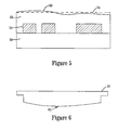
- Figure 6 is a cross-sectional view of a base plate of the present invention.
- the present invention addresses the problem of non-uniformly planarized surfaces upon employing conventional CMP techniques and apparatus, i.e., the resulting surface is characterized by deviations from uniform planarization as, for example, illustrated in Fig. 5 by deviations 53.
- a non-uniformly planarized surface of a patterned wafer adversely affects the reliability of the resulting semiconductor device, particularly a device comprising multi-level vias wherein the shallow vias would be overetched to insure complete etching at the deeper levels.
- the uniformity of surfaces of patterned semiconductor wafers planarized by CMP is markedly improved by modifying the base plate of a conventional carrier assembly to provide a convex portion surface.
- the base plate 60 of the present invention is provided with a convex surface portion 61.
- a carrier film (not shown) is affixed to the surface of the base plate having the convex surface portion 61, and a wafer positioned on the carrier film.
- a retaining ring and vacuum passages are preferably provided, as known in the art.
- the convex portion 61 protrudes so that, during CMP polishing, the center portion of the patterned wafer is polished at a faster rate vis-à-vis the edge portions of the wafer, thereby avoiding non-uniform planarization which would otherwise occur, as shown in Fig. 5, employing a conventional base plate having an essentially flat surface to which the carrier film is affixed as depicted in Fig. 3.
- the carrier assembly comprises a base plate having a convex surface portion made of metal, preferably stainless steel.
- the carrier assembly preferably comprises a retaining ring, preferably made of plastic, which is affixed to the base plate by means of screws in a conventional manner. Vacuum passages are provided in the base plate as well as carrier film to facilitate manipulation of the wafer, as by facilitating transport of the wafer to and from the polishing pad of the CMP apparatus.
- the curvature of the convex surface portion of the base plate is optimized for a particular CMP situation.
- One having ordinary skill in the art would recognize that the optimum radius of curvature depends upon, inter alia , the nature and size of the particular patterned wafer undergoing CMP and the CMP apparatus and process parameters. It has been found that a curvature of the convex surface portion of the base plate having a sagitta of about 1 to about 25 microns, preferably a sagitta of about 5 to about 15 microns, employing a 5 inch spherometer, is suitable.
- the radius of curvature can be calculated from the sagitta and spherometer dimension using known mathematical relationships, as disclosed in " Applied Optics " by Levi, John Wiley & Sons, 1968, pp. 424-425.
- the convex surface portion of the base plate can be formed by modifying a conventional base plate using techniques, such as machining.
- the base plate can be directly manufactured with a convex surface portion by conventional techniques.
- a base plate having a convex surface portion enables the planarization of surfaces of patterned semiconductor wafers by CMP with greatly improved uniformity.
- the present invention also advantageously extends the life of the carrier film without any adverse effect on the CMP removal rate or planarity.
- the carrier film exerts a major influence of surfaces planarized by CMP.
- the usual life of a carrier film employing a conventional base plate having an essentially flat surface is approximately 200-300 wafers.
- the life of a carrier film is extended to in excess of 500, and even in excess of 1000 wafers. This dramatic improvement in the life of a carrier film results in a significant decrease in equipment downtime and increases throughput considerably.
- the present invention can be practiced employing otherwise conventional CMP techniques and, otherwise conventional CMP apparatus.
- CMP apparatus disclosed in the previously mentioned Gill, Jr . or Walsh patents can be employed in the practice of the present invention.
- the polishing pad employed can be any of those which are conventionally employed in CMP, such as those comprising a cellular polyurethane pad.
- the cleaning agent employed can be any of those conventionally employed in CMP processing; preferably, the cleaning agent comprises a slurry.
- the carrier film employed can be any of those commercially available. For example, DF200 and R200, available from Rodel, Newark, Delaware, are suitable.
- the CMP apparatus and method are applicable to a wide variety of situations which require planarization during the course of manufacturing a semiconductor device.
- the improved CMP method and apparatus of the present invention greatly improves the uniformity of planarized patterned semiconductor wafers, advantageously reduces equipment downtime and production cost, while simplifying manufacturing and improving the reliability of the resulting semiconductor devices.
- the present invention enjoys utility in planarizing various types of surfaces on a patterned semiconductor wafer, including conductive and insulating materials, such as oxides, nitrides, polysilicon, single crystalline silicon, amorphous silicon, and mixtures thereof.
- the substrate of the patterned wafer containing the conductive or non-conductive material is generally a semiconductor material, such as silicon.
Abstract
Description
- The present invention relates to a carrier assembly for CMP apparatus, as per the preamble of
claim 1. An example of such an apparatus is disclosed by EP 451 471. - Semiconductor integrated circuits are manufactured by forming an array of separate dies on a common semiconductor wafer. During processing, the wafer is treated to form specified regions of insulating, conductive and semiconductor type materials. The ever increasing requirements for high density devices comprising wiring patterns with increasingly smaller distances between conductive lines poses a significant technological challenge. Conventionally, a wiring pattern comprising a dense array of conductive lines is formed by depositing a metal layer and etching to form a conductive pattern. A dielectric is then applied to the wiring pattern and planarization is effected as by chemical-mechanical polishing. However, it is extremely difficult to obtain uniformly planarized layers, particularly with dense arrays of conductive lines separated by small distances, such as less than one micron.
- As shown in Figs. 1A, during an initial processing stage for forming an integrated circuit, a
dielectric film 10 is deposited over a patterned conductive layer, such as ametal 11. The object is to planarizesteps 12 indielectric layer 10, as shown in Fig. 1B. After deposition oflayer 10, the portion thereof outside the trench must be removed. Such removal can be effected by plasma etching, or by a simplified faster and relatively inexpensive method known as chemical-mechanical planarization or polishing (CMP) . - CMP is a conventional technique as disclosed in, for example, Salugsugan, U.S. Patent No. 5,245,794; Beyer et al ., U.S. Patent No. 4,944,836; Youmans , U.S. Patent No. 3,911,562. CMP is discussed in relation to earlier methods of fabricating metal interconnect structures by Kaufman et al. in "Chemical-Mechanical Polishing for Fabricating Patterned W Metal Features as Chip Interconnects," J. Electrochem. Soc., Vol. 138, No. 11, November 1991, pp. 3460-3464. U.S. Patent No. 4,193,226 and 4,811,522 to Gill, Jr. and U.S. Patent No. 3,841,031 to Walsh relate to CMP apparatus.
- Basically, in employing a conventional CMP apparatus, wafers to be polished are mounted on a carrier assembly which is placed on the CMP apparatus. A polishing pad is adapted to engage the wafers carried by the carrier assembly. A chemical agent containing an abrasive, typically a slurry, is dripped onto the pad continuously during the polishing operation while pressure is applied to the wafer via the carrier assembly.
- A
typical CMP apparatus 100 is shown in Fig. 2 and comprises arotatable polishing platen 102,polishing pad 104 mounted onplaten 102, driven by microprocessor control motor (not shown) to spin at about 10 to about 100 RPM. Wafer 106 is mounted on the bottom of arotatable carrier assembly 108 so that a major surface ofwafer 106 to be polished is positionable to contact the underlyingpolishing pad 104.Wafer 106 andcarrier assembly 108 are attached to avertical spindle 110 which is rotatably mounted in a lateralrobotic arm 112 which rotates thecarrier assembly 108 at about 10 to about 75 RPM in the same direction asplaten 102 and radially positions the carrier assembly on the platen.Robotic arm 112 also verticallypositions carrier assembly 108 to bringwafer 106 into contact withpolishing pad 104 and maintain an appropriate polishing contact pressure. Atube 114opposite carrier assembly 108 abovepolishing pad 104 dispenses and evenly saturates the pad with anappropriate cleaning agent 116, typically a slurry. - The carrier assembly normally employed in a CMP apparatus, such as that depicted in Fig. 2, is shown in Fig. 3 and typically comprises a
base plate 30, to which acarrier film 32 is affixed, and aretaining ring 34.Patterned semiconductor wafer 33 is positioned against thecarrier film 32 and a downward pressure is applied in the direction of thearrow 35. Thebase plate 30 is typically made of metal, such as stainless steel, while theretaining ring 34 is typically made of plastic and is mounted to thebase plate 30 with screws (not shown). Conventionally, the base plate is provided with passages (not shown) through which a vacuum is applied to enable manipulation and transport of the patterned wafer to and from the polishing pad. - It is difficult to obtain a uniformly planarized surface employing conventional CMP techniques and apparatus, particularly of a high density conductive pattern with spacings filled with a dielectric material. For example, as shown in Fig. 5, conventional CMP of a patterned
wafer 50 havingmetal pattern 51 and dielectric 52 undesirably results indeviations 53 from a desirableuniform planarization 54. - Upon initially installing a carrier film on a carrier apparatus of a CMP apparatus, a test wafer is conventionally evaluated for polishing rate and surface uniformity. Planarization by CMP is conducted with the carrier apparatus to process the wafer until the non-uniformity value exceeds the specification limit. A normal failure mode for non-uniformity is a wafer which is polished to a greater extent on the edges than in the center of the wafer. Fig. 4, illustrates a
test wafer 40 planarized by CMP and evaluated by a conventional nine point program for thickness measurements. The points in the center of the wafer, e.g. points 1-5, have a higher post polishing thickness vis-á-vis the edge portions identified by points 6-9. - The problem of non-uniform planarization resulting from conventional CMP techniques and apparatus is recognized in the semiconductor industry. See Ali et al. "Chemical-mechanical polishing of interlayer dielectric: A review," Solid-State Technology, October 1994, pp. 63-68. Previous attempts to solve this problem focus upon improvements in the consumable materials employed during CMP, such as the polishing pad and cleaning agent, or improvements in the hardware itself, such as the CMP apparatus.
- In EP-A-451 471 the lower flat portion of a wafer carrier is formed of a material having a higher coefficient of thermal expansion than the upper flat portion thereof. Upon elevating the temperature. a convex bias is provided to the wafer due to the difference in coefficients of thermal expansion.
- An object of the present invention is a CMP method and apparatus for planarizing a surface on a patterned wafer, wherein the planarized surface exhibits improved uniformity.
- Additional objects, advantages and other features of the invention will be set forth in part in the description which follows and in part will become apparent to those having ordinary skill in the art upon examination of the following or may be learned from practice of the invention. The objects and advantages of the invention may be realized and attained as particularly pointed out in the appended claims.
- The present invention provides a carrier assembly for a chemical-mechanical polishing apparatus for planarizing a semiconductor wafer, which carrier assembly comprises a base plate, characterised in that
the base plate is manufactured with a convex surface portion with a radius of curvature having a sagitta of about 1 to about 25 microns, measured using a 127 mm (5 inch) spherometer. - The present invention also provides a method of manufacturing a semiconductor device comprising planarizing a patterned wafer by chemical-mechanical polishing, which method comprises applying pressure to the patterned wafer by means of a carrier assembly as set out in the preceding paragraph.
- Additional objects and advantages of the present invention will become readily apparent to those skilled in this art from the following detailed description, wherein only the preferred embodiment of the invention is shown and described, simply by way of illustration of the best mode contemplated for carrying out the invention. As will be realized, the invention is capable of other and different embodiments, and its several details are capable of modifications in various obvious respects, all without departing from the invention. Accordingly, the drawings and description are to be regarded as illustrative in nature, and not as restrictive.
- Figure 1A schematically illustrates a covered pattern prior to planarization.
- Figure 1B schematically illustrates a planarized pattern.
- Figure 2 schematically illustrates a typical CMP machine.
- Figure 3 depicts a conventional carrier assembly.
- Figure 4 represents a wafer test pattern illustrating a non-uniform planarization problem addressed by the invention.
- Figure 5 schematically illustrates a non-uniform planarization problem addressed by the present invention.
- Figure 6 is a cross-sectional view of a base plate of the present invention.
- The present invention addresses the problem of non-uniformly planarized surfaces upon employing conventional CMP techniques and apparatus, i.e., the resulting surface is characterized by deviations from uniform planarization as, for example, illustrated in Fig. 5 by
deviations 53. A non-uniformly planarized surface of a patterned wafer adversely affects the reliability of the resulting semiconductor device, particularly a device comprising multi-level vias wherein the shallow vias would be overetched to insure complete etching at the deeper levels. In accordance with the present invention, the uniformity of surfaces of patterned semiconductor wafers planarized by CMP is markedly improved by modifying the base plate of a conventional carrier assembly to provide a convex portion surface. - As shown in Fig. 6, the
base plate 60 of the present invention is provided with aconvex surface portion 61. In use, a carrier film (not shown) is affixed to the surface of the base plate having theconvex surface portion 61, and a wafer positioned on the carrier film. A retaining ring and vacuum passages are preferably provided, as known in the art. - When employing the base plate of the present invention, as shown in Fig. 6, the
convex portion 61 protrudes so that, during CMP polishing, the center portion of the patterned wafer is polished at a faster rate vis-à-vis the edge portions of the wafer, thereby avoiding non-uniform planarization which would otherwise occur, as shown in Fig. 5, employing a conventional base plate having an essentially flat surface to which the carrier film is affixed as depicted in Fig. 3. - The carrier assembly comprises a base plate having a convex surface portion made of metal, preferably stainless steel. The carrier assembly preferably comprises a retaining ring, preferably made of plastic, which is affixed to the base plate by means of screws in a conventional manner. Vacuum passages are provided in the base plate as well as carrier film to facilitate manipulation of the wafer, as by facilitating transport of the wafer to and from the polishing pad of the CMP apparatus.
- The curvature of the convex surface portion of the base plate is optimized for a particular CMP situation. One having ordinary skill in the art would recognize that the optimum radius of curvature depends upon, inter alia , the nature and size of the particular patterned wafer undergoing CMP and the CMP apparatus and process parameters. It has been found that a curvature of the convex surface portion of the base plate having a sagitta of about 1 to about 25 microns, preferably a sagitta of about 5 to about 15 microns, employing a 5 inch spherometer, is suitable. The radius of curvature can be calculated from the sagitta and spherometer dimension using known mathematical relationships, as disclosed in "Applied Optics" by Levi, John Wiley & Sons, 1968, pp. 424-425.
- The convex surface portion of the base plate can be formed by modifying a conventional base plate using techniques, such as machining. Alternatively, the base plate can be directly manufactured with a convex surface portion by conventional techniques.
- A base plate having a convex surface portion enables the planarization of surfaces of patterned semiconductor wafers by CMP with greatly improved uniformity. The present invention also advantageously extends the life of the carrier film without any adverse effect on the CMP removal rate or planarity. The carrier film exerts a major influence of surfaces planarized by CMP. The usual life of a carrier film employing a conventional base plate having an essentially flat surface is approximately 200-300 wafers. However, upon employing the base plate having a convex surface portion, it was found that the life of a carrier film is extended to in excess of 500, and even in excess of 1000 wafers. This dramatic improvement in the life of a carrier film results in a significant decrease in equipment downtime and increases throughput considerably.
- The present invention can be practiced employing otherwise conventional CMP techniques and, otherwise conventional CMP apparatus. For example, the CMP apparatus disclosed in the previously mentioned Gill, Jr. or Walsh patents can be employed in the practice of the present invention.
- An optimum initial pressure is selected to obtain effective removal of material at an economically desirable high rate of speed, typically between about 6 and about 10 psi. The polishing pad employed can be any of those which are conventionally employed in CMP, such as those comprising a cellular polyurethane pad. The cleaning agent employed can be any of those conventionally employed in CMP processing; preferably, the cleaning agent comprises a slurry. The carrier film employed can be any of those commercially available. For example, DF200 and R200, available from Rodel, Newark, Delaware, are suitable.
- The CMP apparatus and method are applicable to a wide variety of situations which require planarization during the course of manufacturing a semiconductor device. The improved CMP method and apparatus of the present invention greatly improves the uniformity of planarized patterned semiconductor wafers, advantageously reduces equipment downtime and production cost, while simplifying manufacturing and improving the reliability of the resulting semiconductor devices. The present invention enjoys utility in planarizing various types of surfaces on a patterned semiconductor wafer, including conductive and insulating materials, such as oxides, nitrides, polysilicon, single crystalline silicon, amorphous silicon, and mixtures thereof. The substrate of the patterned wafer containing the conductive or non-conductive material is generally a semiconductor material, such as silicon.
Claims (16)
- A carrier assembly for a chemical-mechanical polishing apparatus for planarizing a semiconductor wafer, which carrier assembly comprises a base plate (60), characterised in that
the base plate has a convex surface portion (61) with a radius of curvature, at about room temperature, having a sagitta of about 1 to about 25 microns, measured using a 127 mm (5 inch) spherometer. - The carrier assembly according to claim 1, wherein the curvature has a sagitta of about 5 to about 15 microns.
- The carrier assembly according to any of claims 1 to 2 wherein the base plate is of a single metal
- The carrier assembly according to any of claims 1 to 3 wherein the base plate is of stainless steel.
- The carrier assembly according to any of claims 1 to 4, further comprising a carrier film (32) affixed to a surface of the base plate having the convex surface portion.
- The carrier assembly according to any of claims 1 to 4 further comprising a retaining ring (34)
- The carrier assembly according to claim 5, wherein the base plate and carrier film include vacuum passages.
- A chemical-mechanical polishing apparatus comprising a carrier assembly according to claim 1.
- The chemical-mechanical polishing apparatus according to claim 8, further comprising a polishing pad.
- A method of manufacturing a semiconductor device comprising planarizing a patterned wafer by chemical-mechanical polishing, which method comprises applying pressure to the patterned wafer by means of a carrier assembly as claimed in any of claims 1 to 7.
- The method according to claim 10, wherein the carrier assembly further comprises a carrier film (32) affixed the surface of the base plate having the convex surface portion, and wherein pressure is applied to the patterned wafer via the carrier film.
- The method according to claims 10 to 11, wherein the patterned wafer comprises an insulating pattern.
- The method according to claims 10 to 11, wherein the patterned wafer comprises a conductive pattern.
- The method according to any of claims 10 to 13, comprising chemical-mechanical polishing the patterned wafer on a polishing pad.
- The method according to claim 14, comprising applying a cleaning agent to the polishing pad during chemical-mechanical polishing.
- The method according to claim 15, wherein the cleaning agent is a slurry.
Applications Claiming Priority (3)
| Application Number | Priority Date | Filing Date | Title |
|---|---|---|---|
| US38742495A | 1995-02-10 | 1995-02-10 | |
| PCT/US1996/000152 WO1996024467A1 (en) | 1995-02-10 | 1996-01-11 | Chemical-mechanical polishing using curved carriers |
| US387424 | 1999-08-31 |
Publications (2)
| Publication Number | Publication Date |
|---|---|
| EP0808231A1 EP0808231A1 (en) | 1997-11-26 |
| EP0808231B1 true EP0808231B1 (en) | 2000-11-02 |
Family
ID=23529807
Family Applications (1)
| Application Number | Title | Priority Date | Filing Date |
|---|---|---|---|
| EP96902099A Expired - Lifetime EP0808231B1 (en) | 1995-02-10 | 1996-01-11 | Chemical-mechanical polishing using curved carriers |
Country Status (5)
| Country | Link |
|---|---|
| US (1) | US5766058A (en) |
| EP (1) | EP0808231B1 (en) |
| DE (1) | DE69610821T2 (en) |
| TW (1) | TW301771B (en) |
| WO (1) | WO1996024467A1 (en) |
Families Citing this family (14)
| Publication number | Priority date | Publication date | Assignee | Title |
|---|---|---|---|---|
| JPH10235552A (en) * | 1997-02-24 | 1998-09-08 | Ebara Corp | Polishing device |
| US6074288A (en) * | 1997-10-30 | 2000-06-13 | Lsi Logic Corporation | Modified carrier films to produce more uniformly polished substrate surfaces |
| US5961375A (en) * | 1997-10-30 | 1999-10-05 | Lsi Logic Corporation | Shimming substrate holder assemblies to produce more uniformly polished substrate surfaces |
| US6142857A (en) * | 1998-01-06 | 2000-11-07 | Speedfam-Ipec Corporation | Wafer polishing with improved backing arrangement |
| US6113466A (en) * | 1999-01-29 | 2000-09-05 | Taiwan Semiconductor Manufacturing Co., Ltd. | Apparatus and method for controlling polishing profile in chemical mechanical polishing |
| US6309277B1 (en) * | 1999-03-03 | 2001-10-30 | Advanced Micro Devices, Inc. | System and method for achieving a desired semiconductor wafer surface profile via selective polishing pad conditioning |
| US6217418B1 (en) | 1999-04-14 | 2001-04-17 | Advanced Micro Devices, Inc. | Polishing pad and method for polishing porous materials |
| US6722963B1 (en) | 1999-08-03 | 2004-04-20 | Micron Technology, Inc. | Apparatus for chemical-mechanical planarization of microelectronic substrates with a carrier and membrane |
| US6467120B1 (en) | 1999-09-08 | 2002-10-22 | International Business Machines Corporation | Wafer cleaning brush profile modification |
| JP3342686B2 (en) * | 1999-12-28 | 2002-11-11 | 信越半導体株式会社 | Wafer polishing method and wafer polishing apparatus |
| US6786809B1 (en) * | 2001-03-30 | 2004-09-07 | Cypress Semiconductor Corp. | Wafer carrier, wafer carrier components, and CMP system for polishing a semiconductor topography |
| US6761619B1 (en) | 2001-07-10 | 2004-07-13 | Cypress Semiconductor Corp. | Method and system for spatial uniform polishing |
| DE10214272B4 (en) * | 2002-03-28 | 2004-09-02 | Forschungszentrum Jülich GmbH | Holder for a wafer |
| KR20220009216A (en) * | 2020-07-15 | 2022-01-24 | 삼성전자주식회사 | Light emitting device, method of manufacturing the light emitting device, and display apparatus including the light emitting device |
Family Cites Families (21)
| Publication number | Priority date | Publication date | Assignee | Title |
|---|---|---|---|---|
| US3841031A (en) * | 1970-10-21 | 1974-10-15 | Monsanto Co | Process for polishing thin elements |
| US3888053A (en) * | 1973-05-29 | 1975-06-10 | Rca Corp | Method of shaping semiconductor workpiece |
| US3911562A (en) * | 1974-01-14 | 1975-10-14 | Signetics Corp | Method of chemical polishing of planar silicon structures having filled grooves therein |
| US4009539A (en) * | 1975-06-16 | 1977-03-01 | Spitfire Tool & Machine Co., Inc. | Lapping machine with vacuum workholder |
| US4193226A (en) * | 1977-09-21 | 1980-03-18 | Kayex Corporation | Polishing apparatus |
| US4508161A (en) * | 1982-05-25 | 1985-04-02 | Varian Associates, Inc. | Method for gas-assisted, solid-to-solid thermal transfer with a semiconductor wafer |
| US4944836A (en) * | 1985-10-28 | 1990-07-31 | International Business Machines Corporation | Chem-mech polishing method for producing coplanar metal/insulator films on a substrate |
| US4724222A (en) * | 1986-04-28 | 1988-02-09 | American Telephone And Telegraph Company, At&T Bell Laboratories | Wafer chuck comprising a curved reference surface |
| JPS63232953A (en) * | 1987-03-19 | 1988-09-28 | Canon Inc | Polishing tool |
| US4811522A (en) * | 1987-03-23 | 1989-03-14 | Gill Jr Gerald L | Counterbalanced polishing apparatus |
| US5291692A (en) * | 1989-09-14 | 1994-03-08 | Olympus Optical Company Limited | Polishing work holder |
| US5234867A (en) * | 1992-05-27 | 1993-08-10 | Micron Technology, Inc. | Method for planarizing semiconductor wafers with a non-circular polishing pad |
| US5036630A (en) * | 1990-04-13 | 1991-08-06 | International Business Machines Corporation | Radial uniformity control of semiconductor wafer polishing |
| US5131968A (en) * | 1990-07-31 | 1992-07-21 | Motorola, Inc. | Gradient chuck method for wafer bonding employing a convex pressure |
| DE4108786C2 (en) * | 1991-03-18 | 1995-01-05 | Hydromatik Gmbh | Light pistons for hydrostatic axial and radial piston machines |
| US5069002A (en) * | 1991-04-17 | 1991-12-03 | Micron Technology, Inc. | Apparatus for endpoint detection during mechanical planarization of semiconductor wafers |
| US5245794A (en) * | 1992-04-09 | 1993-09-21 | Advanced Micro Devices, Inc. | Audio end point detector for chemical-mechanical polishing and method therefor |
| EP0911115B1 (en) * | 1992-09-24 | 2003-11-26 | Ebara Corporation | Polishing apparatus |
| DE69316849T2 (en) * | 1992-11-27 | 1998-09-10 | Toshiba Kawasaki Kk | Method and device for polishing a workpiece |
| US5302233A (en) * | 1993-03-19 | 1994-04-12 | Micron Semiconductor, Inc. | Method for shaping features of a semiconductor structure using chemical mechanical planarization (CMP) |
| US5423716A (en) * | 1994-01-05 | 1995-06-13 | Strasbaugh; Alan | Wafer-handling apparatus having a resilient membrane which holds wafer when a vacuum is applied |
-
1996
- 1996-01-11 WO PCT/US1996/000152 patent/WO1996024467A1/en active IP Right Grant
- 1996-01-11 EP EP96902099A patent/EP0808231B1/en not_active Expired - Lifetime
- 1996-01-11 DE DE69610821T patent/DE69610821T2/en not_active Expired - Lifetime
- 1996-01-22 TW TW085100691A patent/TW301771B/zh not_active IP Right Cessation
-
1997
- 1997-01-21 US US08/784,619 patent/US5766058A/en not_active Expired - Lifetime
Also Published As
| Publication number | Publication date |
|---|---|
| EP0808231A1 (en) | 1997-11-26 |
| US5766058A (en) | 1998-06-16 |
| DE69610821D1 (en) | 2000-12-07 |
| WO1996024467A1 (en) | 1996-08-15 |
| TW301771B (en) | 1997-04-01 |
| DE69610821T2 (en) | 2001-06-07 |
Similar Documents
| Publication | Publication Date | Title |
|---|---|---|
| EP0808230B1 (en) | Chemical-mechanical polishing of thin materials using a pulse polishing technique | |
| US6276997B1 (en) | Use of chemical mechanical polishing and/or poly-vinyl-acetate scrubbing to restore quality of used semiconductor wafers | |
| US5665201A (en) | High removal rate chemical-mechanical polishing | |
| US6238271B1 (en) | Methods and apparatus for improved polishing of workpieces | |
| US4879258A (en) | Integrated circuit planarization by mechanical polishing | |
| US5798302A (en) | Low friction polish-stop stratum for endpointing chemical-mechanical planarization processing of semiconductor wafers | |
| EP0808231B1 (en) | Chemical-mechanical polishing using curved carriers | |
| EP0907460B1 (en) | Method for chemical-mechanical planarization of stop-on-feature semiconductor wafers | |
| EP0366027B1 (en) | Wafer flood polishing | |
| US7132035B2 (en) | Methods, apparatuses, and substrate assembly structures for fabricating microelectronic components using mechanical and chemical-mechanical planarization processes | |
| US5702563A (en) | Reduced chemical-mechanical polishing particulate contamination | |
| US5609719A (en) | Method for performing chemical mechanical polish (CMP) of a wafer | |
| US20080268643A1 (en) | Methods and apparatus for polishing control | |
| US6150271A (en) | Differential temperature control in chemical mechanical polishing processes | |
| JP2870537B1 (en) | Polishing apparatus and method for manufacturing semiconductor device using the same | |
| US5769696A (en) | Chemical-mechanical polishing of thin materials using non-baked carrier film | |
| US6213844B1 (en) | Method for obtaining a desired film thickness using chemical mechanical polishing | |
| US6736696B2 (en) | Method of improving uniformity control on wafers during chemical mechanical polishing | |
| US6593238B1 (en) | Method for determining an endpoint and semiconductor wafer | |
| US5736463A (en) | Method and apparatus for chemical/mechanical polishing | |
| US6387808B1 (en) | Method of correcting topographical effects on a micro-electronic substrate | |
| US6347977B1 (en) | Method and system for chemical mechanical polishing | |
| US20030134576A1 (en) | Method for polishing copper on a workpiece surface | |
| US6080671A (en) | Process of chemical-mechanical polishing and manufacturing an integrated circuit | |
| CN100369212C (en) | CMP polishing method and method for manufacturing semiconductor device |
Legal Events
| Date | Code | Title | Description |
|---|---|---|---|
| PUAI | Public reference made under article 153(3) epc to a published international application that has entered the european phase |
Free format text: ORIGINAL CODE: 0009012 |
|
| 17P | Request for examination filed |
Effective date: 19970901 |
|
| AK | Designated contracting states |
Kind code of ref document: A1 Designated state(s): DE FR GB NL |
|
| 17Q | First examination report despatched |
Effective date: 19980909 |
|
| GRAG | Despatch of communication of intention to grant |
Free format text: ORIGINAL CODE: EPIDOS AGRA |
|
| GRAG | Despatch of communication of intention to grant |
Free format text: ORIGINAL CODE: EPIDOS AGRA |
|
| GRAH | Despatch of communication of intention to grant a patent |
Free format text: ORIGINAL CODE: EPIDOS IGRA |
|
| GRAH | Despatch of communication of intention to grant a patent |
Free format text: ORIGINAL CODE: EPIDOS IGRA |
|
| GRAA | (expected) grant |
Free format text: ORIGINAL CODE: 0009210 |
|
| AK | Designated contracting states |
Kind code of ref document: B1 Designated state(s): DE FR GB NL |
|
| REF | Corresponds to: |
Ref document number: 69610821 Country of ref document: DE Date of ref document: 20001207 |
|
| ET | Fr: translation filed | ||
| PLBE | No opposition filed within time limit |
Free format text: ORIGINAL CODE: 0009261 |
|
| STAA | Information on the status of an ep patent application or granted ep patent |
Free format text: STATUS: NO OPPOSITION FILED WITHIN TIME LIMIT |
|
| 26N | No opposition filed | ||
| PGFP | Annual fee paid to national office [announced via postgrant information from national office to epo] |
Ref country code: NL Payment date: 20011214 Year of fee payment: 7 |
|
| REG | Reference to a national code |
Ref country code: GB Ref legal event code: IF02 |
|
| PG25 | Lapsed in a contracting state [announced via postgrant information from national office to epo] |
Ref country code: NL Free format text: LAPSE BECAUSE OF NON-PAYMENT OF DUE FEES Effective date: 20030801 |
|
| NLV4 | Nl: lapsed or anulled due to non-payment of the annual fee |
Effective date: 20030801 |
|
| REG | Reference to a national code |
Ref country code: GB Ref legal event code: 732E Free format text: REGISTERED BETWEEN 20091210 AND 20091216 |
|
| REG | Reference to a national code |
Ref country code: FR Ref legal event code: TP |
|
| PGFP | Annual fee paid to national office [announced via postgrant information from national office to epo] |
Ref country code: FR Payment date: 20101221 Year of fee payment: 16 |
|
| PGFP | Annual fee paid to national office [announced via postgrant information from national office to epo] |
Ref country code: GB Payment date: 20101215 Year of fee payment: 16 |
|
| PGFP | Annual fee paid to national office [announced via postgrant information from national office to epo] |
Ref country code: DE Payment date: 20110131 Year of fee payment: 16 |
|
| GBPC | Gb: european patent ceased through non-payment of renewal fee |
Effective date: 20120111 |
|
| REG | Reference to a national code |
Ref country code: FR Ref legal event code: ST Effective date: 20120928 |
|
| PG25 | Lapsed in a contracting state [announced via postgrant information from national office to epo] |
Ref country code: DE Free format text: LAPSE BECAUSE OF NON-PAYMENT OF DUE FEES Effective date: 20120801 Ref country code: GB Free format text: LAPSE BECAUSE OF NON-PAYMENT OF DUE FEES Effective date: 20120111 |
|
| REG | Reference to a national code |
Ref country code: DE Ref legal event code: R119 Ref document number: 69610821 Country of ref document: DE Effective date: 20120801 |
|
| PG25 | Lapsed in a contracting state [announced via postgrant information from national office to epo] |
Ref country code: FR Free format text: LAPSE BECAUSE OF NON-PAYMENT OF DUE FEES Effective date: 20120131 |