EP0808060B1 - Amplifier circuit with filter for digital and analog signals - Google Patents
Amplifier circuit with filter for digital and analog signals Download PDFInfo
- Publication number
- EP0808060B1 EP0808060B1 EP97107281A EP97107281A EP0808060B1 EP 0808060 B1 EP0808060 B1 EP 0808060B1 EP 97107281 A EP97107281 A EP 97107281A EP 97107281 A EP97107281 A EP 97107281A EP 0808060 B1 EP0808060 B1 EP 0808060B1
- Authority
- EP
- European Patent Office
- Prior art keywords
- filter
- amplifier circuit
- digital
- signal
- analog
- Prior art date
- Legal status (The legal status is an assumption and is not a legal conclusion. Google has not performed a legal analysis and makes no representation as to the accuracy of the status listed.)
- Expired - Lifetime
Links
Images


Classifications
-
- H—ELECTRICITY
- H04—ELECTRIC COMMUNICATION TECHNIQUE
- H04N—PICTORIAL COMMUNICATION, e.g. TELEVISION
- H04N5/00—Details of television systems
- H04N5/44—Receiver circuitry for the reception of television signals according to analogue transmission standards
- H04N5/4446—IF amplifier circuits specially adapted for B&W TV
-
- H—ELECTRICITY
- H04—ELECTRIC COMMUNICATION TECHNIQUE
- H04N—PICTORIAL COMMUNICATION, e.g. TELEVISION
- H04N21/00—Selective content distribution, e.g. interactive television or video on demand [VOD]
- H04N21/40—Client devices specifically adapted for the reception of or interaction with content, e.g. set-top-box [STB]; Operations thereof
- H04N21/41—Structure of client; Structure of client peripherals
- H04N21/426—Internal components of the client ; Characteristics thereof
-
- H—ELECTRICITY
- H04—ELECTRIC COMMUNICATION TECHNIQUE
- H04N—PICTORIAL COMMUNICATION, e.g. TELEVISION
- H04N5/00—Details of television systems
- H04N5/44—Receiver circuitry for the reception of television signals according to analogue transmission standards
- H04N5/46—Receiver circuitry for the reception of television signals according to analogue transmission standards for receiving on more than one standard at will
Description
Die Erfindung geht aus von einer Verstärkerschaltung mit
Filtern für digitale und analoge Signale gemäß dem Oberbegriff
des Anspruchs 1. Multistandard-ZF-Verstärker (ZF =
Zwischenfrequenz) dienen zum analogen Empfang für
unterschiedliche Normen. Für jede Norm muß der ZF-Verstärker
entsprechende Signale selektieren. Die Selektion geschieht im ZF-Bereich
auf einer jeweils festeingestellten Frequenz. Für die
Selektion werden Filter verwendet. Bei analogem Empfang wird eine
Nyquist Flanke benötigt, um ein geeignetes Signal zu gewinnen.
Bei einem digitalen Signal ist dieses nicht notwendig.The invention is based on an amplifier circuit
Filters for digital and analog signals according to the generic term
of
Aus der EP-A 0 006 510 ist ein ZF-Verstärker für Mehrnormen-Fernsehempfänger
bekannt. Bei dem bekannten Verstärker wird für
alle Normen dasselbe Oberflächenwellenfilter verwendet.From EP-
Aus der DE-A 44 27 396 ist ein Verfahren zur Verarbeitung von digitalen und analogen Eingangssignalen bekannt. Bei diesem Verfahren werden abhängig davon, ob digitale oder analoge Signale empfangen werden, einem Schwingungserzeuger unterschiedliche Bauelemente zugeschaltet.DE-A 44 27 396 describes a processing method known from digital and analog input signals. With this Procedures become dependent on whether digital or analog signals be received, a vibration generator different Components switched on.
Bei einer bekannten in Fig. 1 dargestellten Signalverarbeitungsstufe, die analoge und digitale Signale verarbeitet, wird in Abhängigkeit vom empfangenen Signal der entsprechende analoge oder digitale Signalpfad geschaltet. Nachteilig hierbei ist der relativ hohe Aufwand für die analoge Signalverarbeitung.In a known one shown in Fig. 1 Signal processing stage, the analog and digital signals processed, depending on the received signal corresponding analog or digital signal path switched. The disadvantage here is the relatively high cost of the analog Signal processing.
Der Erfindung liegt die Aufgabe zugrunde mit geringem
Aufwand eine Schaltung zu schaffen, die sowohl analoge als auch
digitale Signale verarbeitet. Diese Aufgabe wird durch eine
Verstärkerschaltung gemäß Anspruch 1 gelöst. Vorteilhafte
Weiterbildungen der Erfindung sind in den Unteransprüchen
angegeben. The invention has for its object with little
Effort to create a circuit that is both analog as well
digital signals processed. This task is accomplished by a
Amplifier circuit according to
Erfindungsgemäß werden Filter für digitale und analoge Signale verwendet. Die Filter für digitalen Signalempfang werden bei analogem Signalempfang den analogen Filtern zugeschaltet. Durch das Hinzuschalten der digitalen Filter vor das analoge Filter ist es möglich, auf ansonsten zusätzlich zur Hauptselektion benötigte Selektionsmittel für das analoge Signal zu verzichten. Bei digitalem Signalempfang werden die analogen Filter nicht zugeschaltet, da das digitale Signal die größtmögliche Bandbreite benötigt, das analoge Filter jedoch die Bandbreite begrenzen würde. Zum Entkoppeln der Filter für analoge und digitale Signalverarbeitung wird eine Entkopplungsstufe verwendet. Die Entkopplungsstufe ist vorzugsweise als Emitterfolger ausgebildet. Die Filter für analoge und digitale Signalverarbeitung werden aus Oberflächenwellenfiltern gebildet. Die Filter werden vorzugsweise in Kaskadenschaltung angeordnet.According to the invention, filters for digital and analog Signals used. The filters for digital signal reception are connected to the analog filters for analog signal reception. By connecting the digital filter in front of the analog one It is possible to filter in addition to Main selection required selection means for the analog signal to renounce. With digital signal reception, the analog Filter not activated because the digital signal requires the largest possible bandwidth, but the analog filter needs the Would limit bandwidth. For decoupling the filters for analog and digital signal processing becomes a decoupling stage used. The decoupling stage is preferably as Emitter follower trained. The filters for analog and digital Signal processing is formed from surface wave filters. The filters are preferably arranged in cascade.
Vorteilhaft bei einer derartigen Anordnung ist, daß die Zusatzselektionsmittel im analogen Signalverarbeitungspfad entfallen können. Diese Zusatzselektion wird nun durch die digitalen Filter durchgeführt.An advantage of such an arrangement is that the Additional selection means in the analog signal processing path can be omitted. This additional selection is now made by the digital filter performed.
Ein weiterer Vorteil ist, daß bei den Oberflächenwellenfiltern Amplitudenfrequenzgang- und Gruppenlaufzeit-Charakteristika unabhängig voneinander gestaltet werden können. Durch die Kaskadenschaltung kann eine erwünschte Gruppenlaufzeit für den analogen Signalausgang flexibler gestaltet werden. Das ist möglich durch die Überlagerung der Gruppenlaufzeiten des analogen und digitalen Oberflächenwellenfilters. Ansonsten unvermeidbare Rippel im Signalverlauf am Ausgang des analogen Oberflächenwellenfilters können durch die Kaskadenschaltung und ihrem gegenphasigen Signalverlauf von dem digitalen Oberflächenwellenfilter HS2 kompensiert werden. Der erwünschte Gruppenlaufzeitverlauf des analogen Oberflächenwellenfilters kann durch den passenden Verlauf von dem digitalen Oberflächenwellenfilter erzielt werden. Another advantage is that the Surface wave filters amplitude frequency response and Group runtime characteristics designed independently of each other can be. By cascading a desired one Group delay for the analog signal output more flexible be designed. This is possible by overlaying the Group runtimes of the analog and digital Surface wave filter. Otherwise inevitable ripples in the Signal curve at the output of the analog surface wave filter can by the cascade connection and its antiphase Signal curve from the digital surface wave filter HS2 be compensated. The desired group runtime of the analog surface wave filter can be matched by the appropriate Course of the digital surface wave filter can be achieved.
Die Erfindung wird im folgenden anhand der Zeichnung erläutert. Darin zeigen
- Fig. 1
- eine bekannte Verstärkerschaltung,
- Fig. 2
- eine erfindungsgemäße Verstärkerschaltung und
- Fig. 3,4
- Weiterbildungen der erfindungsgemäßen Verstärkerschaltung.
- Fig. 1
- a known amplifier circuit,
- Fig. 2
- an amplifier circuit according to the invention and
- Fig. 3.4
- Developments of the amplifier circuit according to the invention.
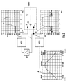
Fig. 1 zeigt eine bekannte Verstärkerschaltung. Das ZF-Signal
vom Tuner, der hier nicht dargestellt ist, gelangt über
den Punkt A in den analogen Pfad 1 und in den digitalen Pfad 2.
Der analoge Pfad 1 wird gebildet aus Selektionsmitteln ZS und dem
Oberflächenwellenfilter HS1. Der digitale Pfad wird gebildet
durch das Oberflächenwellenfilter HS2. Der Schalter S der
Signalverarbeitungsstufe IC schaltet das Signal für den analogen
Empfang bzw. den digitalen Empfang zur Weiterverarbeitung in der
Signalverarbeitungsstufe IC durch. Am Punkt B ist das Signal
dargestellt, welches sich durch das Oberflächenwellenfilter HS2
ergibt. Am Punkt C ist das Signal dargestellt, welches sich durch
die zusätzlichen Selektionsmittel ZS und dem
Oberflächenwellenfilter HS1 ergibt.Fig. 1 shows a known amplifier circuit. The IF signal
from the tuner, which is not shown here, passes through
point A in
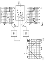
Fig. 2 zeigt die erfindungsgemäße Schaltungsanordnung. Das
ZF Signal des Tuners gelangt vom Punkt A aus über das
Oberflächenwellenfilter HS2 an den Punkt B. Vom Punkt B gelangt
das Signal an den Eingang 4 des Schalters S in der
Signalverarbeitungsstufe IC. Vom Punkt B gelangt das Signal
weiterhin über den Emitterfolger EF an das
Oberflächenwellenfilter HS1. Vom Oberflächenwellenfilter HS1
gelangt das Signal über den Punkt C* an den Eingang 3 des
Schalters S.2 shows the circuit arrangement according to the invention. The
IF signal of the tuner passes from point A via the
Surface wave filter HS2 at point B. Arrived from point B.
the signal to input 4 of switch S in the
IC signal processing stage. The signal comes from point B.
continue via the emitter follower EF to the
Surface wave filter HS1. From the surface wave filter HS1
the signal arrives at
Der Schalter S schaltet in Abhängigkeit von der Art des
empfangenen Signals jeweils auf den Eingang 3 für analoge Signale
oder den Eingang 4 für digitale Signale. Das Umschalten des
Schalters S erfolgt durch die Signalverarbeitungsstufe IC. Die
Unterscheidung, ob ein digitales oder analoges Signal empfangen
wird, ermittelt die Signalverarbeitungsstufe IC aus der
Signalfolge.The switch S switches depending on the type of
received signal to input 3 for analog signals
or
Es ist auch möglich, daß der Benutzer beim Programmieren der
empfangenen Sender der Signalverarbeitungsstufe IC mitteilt, ob
es sich um ein analoges oder digitales Empfangsignal handelt.
Beim späteren Anwählen des Programmplatzes erkennt die
Signalverarbeitungsstufe, daß unter diesem angewählten
Programmplatz ein analoges oder digitales Signal empfangen wird,
und der Schalter wird entsprechend in Schalterstellung 3 oder 4
geschaltet.It is also possible for the user to program the
received transmitter of the signal processing stage IC notifies whether
it is an analog or digital receive signal.
When you later select the program position, the
Signal processing level that selected under this
Program position an analog or digital signal is received,
and the switch is accordingly in
Der Signalverlauf am Punkt A und Punkt B ist unverändert. Am
Punkt C* ist im Vergleich zum Punkt C aus Fig. 1 der
Signalverlauf fast identisch. Der fast identische Signalverlauf
ist erfindungsgemäß angestrebt, damit am Schaltkontakt 3 des
Schalters wiederum ein Signal für die analoge Signalverarbeitung
ansteht. Durch die Kaskadenschaltung der beiden
Oberflächenwellenfilter HS1 und HS2 ist am Punkt C* eine
verbesserte Signalkurve zu sehen.The signal curve at point A and point B is unchanged. At the
Point C * is in comparison to point C from FIG
Signal curve almost identical. The almost identical signal curve
is sought according to the invention so that the switching
Die entfallenen Selektionsmittel ZS dienten zur Unterdrückung von unerwünschten Signalen wie Nachbarträger. Das Oberflächenwellenfilter HS2 hat einen Durchlaßbereich, der größer ist, als der des Oberflächenwellenfilters HS1. Dadurch wird der Durchlaßbereich des Filters HS1 nicht beeinträchtigt. Außerhalb des Durchlaßbereiches wird jedoch eine zusätzliche Selektion erreicht.The deleted selection means ZS were used for Suppression of unwanted signals like neighboring carriers. The Surface wave filter HS2 has a pass band that is larger than that of the surface acoustic wave filter HS1. This will make the Passband of filter HS1 not affected. Outside the passband is an additional selection reached.
Die Selektionsmittel ZS sind also nicht mehr erforderlich, da bei der Kaskadenschaltung der beiden Oberflächenwellenfilter HS2 und HS1 eine Gesamtselektion erreicht wird, die für die analoge Signalverarbeitung verwendbar ist. The selection means ZS are therefore no longer necessary, since the two surface wave filters are cascaded HS2 and HS1 an overall selection is achieved for the analog signal processing can be used.
Fig. 3 zeigt eine Weiterbildung der erfindungsgemäßen Lösung. Der Emitterfolger EF ist in die Signalverarbeitungsstufe IC integriert worden. Die Schaltung arbeitet ansonsten wie unter Fig. 2 beschrieben.3 shows a further development of the invention Solution. The emitter follower EF is in the signal processing stage IC has been integrated. The circuit works otherwise as below Fig. 2 described.
Vorteilhaft ist, daß bei den Oberflächenwellenfilter HS1, HS2 Amplitudenfrequenzgang- und Gruppenlaufzeit-Charakteristika unabhängig voneinander gestaltet werden können. Durch die Kaskadenschaltung kann eine erwünschte Gruppenlaufzeit am Punkt C* (Fig. 2, 3) durch die Überlagerung der Gruppenlaufzeiten in den Oberflächenwellenfiltern HS1, HS2 flexibler gestaltet werden. Ansonsten unvermeidbare Rippel in dem Ausgangssignal des Oberflächenwellenfilters HS1 (Fig. 1, Punkt C), können durch die Kaskadenschaltung durch ihren gegenphasigen Verlauf vom dem Oberflächenwellenfilter HS2 kompensiert werden (Fig. 2,3 Punkt C*). Der erwünschte Gruppenlaufzeitverlauf in dem Oberflächenwellenfilter HS1 kann durch den angepaßten Verlauf von dem Oberflächenwellenfilter HS2 gewonnen werden.It is advantageous that with the surface wave filter HS1, HS2 amplitude frequency response and group delay characteristics can be designed independently. Through the Cascading can create a desired group delay at the point C * (Fig. 2, 3) by superimposing the group delays in the surface wave filters HS1, HS2 can be made more flexible. Otherwise unavoidable ripples in the output signal of the Surface wave filter HS1 (Fig. 1, point C) can by Cascade connection due to its phase opposition from the Surface wave filter HS2 can be compensated (Fig. 2.3 point C *). The desired group runtime in the Surface wave filter HS1 can by the adapted course of the surface wave filter HS2 can be obtained.
Fig. 4 zeigt eine Weiterbildung der erfindungsgemäßen
Schaltung. In dem Schaltbild sind die Baugruppen zusammengefaßt
und markiert worden, die in den vorhergehenden Figuren als Blöcke
dargestellt sind. Die Funktionsweise und das Zusammenarbeiten der
Bauelemente ist anhand der Blockschaltbilder erläutert worden. Es
ist deutlich zu erkennen, daß es nur einen Signaleingang A gibt.
Nach diesem Signaleingang A liegt das Oberflächenwellenfilter HS2
für den digitalen Signalpfad. Anschließend gelangt das Signal zum
Emitterfolger EF und über die Pins 4 und 5 in den integrierten
Schaltkreis IC. Der Meßpunkt B war in den Blockschaltbildern vor
dem Emitterfolger und auch das Signal wurde vor dem Emitterfolger
abgegriffen. In dieser aufgebauten Schaltung wird das Signal
hinter dem Emitterfolger abgegriffen, so daß diese Filter auch
noch für den digitalen Teil ausgenutzt werden können. Der
Signalverlauf am Punkt B ist identisch mit dem Signalverlauf des
vorigen Punktes B aus Fig. 2 und 3. Nach dem Emitterfolger EF
gelangt das Signal zum analogen Oberflächenwellenfilter HS1. Der
analoge Teil ist aufgeteilt in Bild- und Ton und gekennzeichnet
durch die Ausgänge C1 "analog vision" und C2 "analog sound".
Vorteihaft und Unterschiedlich zu Fig. 2 und 3 ist, daß der
Emitterfolger EF sowohl für den digitalen als auch für den
analogen Part verwendet wird.4 shows a further development of the invention
Circuit. The modules are summarized in the circuit diagram
and been marked as blocks in the previous figures
are shown. How it works and how it works
Components have been explained using the block diagrams. It
it can be clearly seen that there is only one signal input A.
The surface wave filter HS2 is located after this signal input A.
for the digital signal path. The signal then arrives at
Emitter follower EF and via
Claims (7)
- Amplifier circuit for IF-signals of different standards for alternatively processing digital or analogue signals includingcharacterized in thatan input (A) for alternatively receiving digital and analogue signals,a first path (2) including a first filter (HS2) for processing digital signals,a second path (1) including a second filter (HS1) for processing analogue signals,the output of the first filter (HS2) is connected to the input of the second filter (HS1),switching means (S) is provided having a first input (4) connected to the output of the first filter (HS2) and having a second input (3) connected to the output of the second filter (HS1) and having an output providing a signal for further processing andsaid switching means (S) is controlled in such a way that during reception of digital signals the first input (4) of said switching means (S) is connected to its output and that during reception of analogue signals the second input (3) of said switching means (S) is connected to its output.
- Amplifier circuit according to claim 1, characterized in that said filters (HS1, HS2) are formed by surface acoustic wave filters.
- Amplifier circuit according to claim 1, characterized in that said filters (HS1, HS2) are arranged in a cascade circuit.
- Amplifier circuit according to claim 1, characterized in that the filters (HS1, HS2) are joined by a decoupling stage (EF).
- Amplifier circuit according to claim 4, characterized in that the decoupling stage (EF) is formed by an emitter follower.
- Amplifier circuit according to claim 2, characterized in that the total group delay time response profile can be altered by the group delay time of said surface acoustic wave filters (HS1, HS2).
- Amplifier circuit according to claim 2, characterized in that the total amplitude frequency response profile can be altered by the amplitude frequency response of the surface acoustic wave filters (HS1, HS2).
Applications Claiming Priority (2)
| Application Number | Priority Date | Filing Date | Title |
|---|---|---|---|
| DE19619750A DE19619750A1 (en) | 1996-05-15 | 1996-05-15 | Amplifier circuit with filter for digital and analog signals |
| DE19619750 | 1996-05-15 |
Publications (3)
| Publication Number | Publication Date |
|---|---|
| EP0808060A2 EP0808060A2 (en) | 1997-11-19 |
| EP0808060A3 EP0808060A3 (en) | 1999-02-24 |
| EP0808060B1 true EP0808060B1 (en) | 2001-12-12 |
Family
ID=7794476
Family Applications (1)
| Application Number | Title | Priority Date | Filing Date |
|---|---|---|---|
| EP97107281A Expired - Lifetime EP0808060B1 (en) | 1996-05-15 | 1997-05-02 | Amplifier circuit with filter for digital and analog signals |
Country Status (4)
| Country | Link |
|---|---|
| EP (1) | EP0808060B1 (en) |
| JP (1) | JP4050354B2 (en) |
| CN (1) | CN1083639C (en) |
| DE (2) | DE19619750A1 (en) |
Families Citing this family (6)
| Publication number | Priority date | Publication date | Assignee | Title |
|---|---|---|---|---|
| AU4477500A (en) * | 1999-04-20 | 2000-11-02 | Thomson Licensing S.A. | If signal processing apparatus |
| US7202910B1 (en) | 1999-04-20 | 2007-04-10 | Thomson Licensing | Signal processing apparatus |
| DE10163798A1 (en) * | 2001-12-22 | 2003-07-03 | Philips Intellectual Property | TV signal receiver with universal output for various surface wave filters |
| JP2008309426A (en) * | 2007-06-15 | 2008-12-25 | Sanden Corp | Heat pump type hot water supply apparatus |
| CN104618666B (en) | 2013-11-05 | 2018-04-10 | 南宁富桂精密工业有限公司 | audio signal control circuit |
| CN105978533A (en) * | 2016-06-18 | 2016-09-28 | 南通尚青医疗科技有限公司 | Composite filter |
Family Cites Families (8)
| Publication number | Priority date | Publication date | Assignee | Title |
|---|---|---|---|---|
| DE3120050A1 (en) * | 1981-05-20 | 1982-12-09 | Licentia Patent-Verwaltungs-Gmbh, 6000 Frankfurt | ZF AMPLIFIER FOR A MULTI-STANDARD TELEVISION RECEIVER |
| US4868516A (en) * | 1988-04-14 | 1989-09-19 | John Fluke Mfg. Co., Inc. | Alternating current amplifier with digitally controlled frequency response |
| US5283653A (en) * | 1992-05-22 | 1994-02-01 | Zenith Electronics Corp. | Dual HDTV/NTSC receiver using sequentially synthesized HDTV and NTSC co-channel carrier frequencies |
| JPH07176912A (en) * | 1993-12-17 | 1995-07-14 | Sanyo Electric Co Ltd | High frequency filter |
| JPH07255016A (en) * | 1994-03-15 | 1995-10-03 | Toshiba Corp | Compatible receiver for analog and digital broadcast |
| JP2905094B2 (en) * | 1994-07-01 | 1999-06-14 | 富士通株式会社 | Demultiplexer package |
| DE4427396A1 (en) * | 1994-08-03 | 1996-02-08 | Thomson Brandt Gmbh | Digital and analogue input signal processing circuit for television signals |
| EP0696854A1 (en) * | 1994-08-08 | 1996-02-14 | THOMSON multimedia S.A. | Broadcast receiver adapted for analog and digital signals |
-
1996
- 1996-05-15 DE DE19619750A patent/DE19619750A1/en not_active Withdrawn
-
1997
- 1997-05-02 EP EP97107281A patent/EP0808060B1/en not_active Expired - Lifetime
- 1997-05-02 DE DE59705730T patent/DE59705730D1/en not_active Expired - Lifetime
- 1997-05-12 CN CN97111153A patent/CN1083639C/en not_active Expired - Lifetime
- 1997-05-14 JP JP12399197A patent/JP4050354B2/en not_active Expired - Lifetime
Also Published As
| Publication number | Publication date |
|---|---|
| JPH1084298A (en) | 1998-03-31 |
| DE19619750A1 (en) | 1997-11-20 |
| EP0808060A2 (en) | 1997-11-19 |
| DE59705730D1 (en) | 2002-01-24 |
| EP0808060A3 (en) | 1999-02-24 |
| CN1166089A (en) | 1997-11-26 |
| CN1083639C (en) | 2002-04-24 |
| JP4050354B2 (en) | 2008-02-20 |
Similar Documents
| Publication | Publication Date | Title |
|---|---|---|
| DE3120050C2 (en) | ||
| EP0808060B1 (en) | Amplifier circuit with filter for digital and analog signals | |
| EP1657917A1 (en) | Method and circuit arrangement for filtering analog or digital modulated TV signals | |
| EP0246698B1 (en) | Circuit arrangement for a television receiver provided with a teletext decoder | |
| EP0889646B1 (en) | Television signal receiver | |
| EP0367864B1 (en) | Surface acoustic wave fibre with variable bandpass characteristics | |
| DE4103061C2 (en) | Radio receiver | |
| EP0105998A1 (en) | Integrated digital filter circuit for the luminance channel of colour television sets | |
| WO1995003650A1 (en) | If filter arrangement for fm reception signals | |
| DE2163247C3 (en) | Device for eliminating the interference signals contained in an input signal | |
| EP0678981A2 (en) | High-frequency receiving stage | |
| DE3701134A1 (en) | Radio receiver with extremely wide bandwidth | |
| DE19731012B4 (en) | Arrangement for generating a vestigial sideband modulated video signal with residual carrier for a television station | |
| DE4019579C2 (en) | Circuit for processing video signals and automatic fine-tuning signals to match the respective broadcasting system | |
| EP0642713B1 (en) | Circuit for deriving a signal indicating interference in a received stereo multiplex signal | |
| DE3808917C2 (en) | ||
| DE3525556A1 (en) | VOTING | |
| DE3823124C2 (en) | ||
| DE2738068C2 (en) | Radio or television receiver | |
| DE1012326B (en) | Device for delaying drawing voltages | |
| DE2537137C3 (en) | Circuit arrangement for suppressing interfering received signals in a pulse Doppler radar receiver | |
| DE2927772A1 (en) | TV receiver control circuit - has filter separating synchronising signal for intermediate frequency amplifier using strobing logic gate | |
| DE10163798A1 (en) | TV signal receiver with universal output for various surface wave filters | |
| DE4029463A1 (en) | TV receiver demodulation circuit - has combined T-bridge blocking circuit stage with parallel circuits for UHF and VHF bands | |
| DE2751933A1 (en) | BANDWIDTH CIRCUIT FOR RADIO RECEIVER |
Legal Events
| Date | Code | Title | Description |
|---|---|---|---|
| PUAI | Public reference made under article 153(3) epc to a published international application that has entered the european phase |
Free format text: ORIGINAL CODE: 0009012 |
|
| AK | Designated contracting states |
Kind code of ref document: A2 Designated state(s): DE FR GB IT |
|
| PUAL | Search report despatched |
Free format text: ORIGINAL CODE: 0009013 |
|
| AK | Designated contracting states |
Kind code of ref document: A3 Designated state(s): DE FR GB IT |
|
| 17P | Request for examination filed |
Effective date: 19990710 |
|
| 17Q | First examination report despatched |
Effective date: 19990901 |
|
| GRAG | Despatch of communication of intention to grant |
Free format text: ORIGINAL CODE: EPIDOS AGRA |
|
| GRAG | Despatch of communication of intention to grant |
Free format text: ORIGINAL CODE: EPIDOS AGRA |
|
| GRAH | Despatch of communication of intention to grant a patent |
Free format text: ORIGINAL CODE: EPIDOS IGRA |
|
| GRAH | Despatch of communication of intention to grant a patent |
Free format text: ORIGINAL CODE: EPIDOS IGRA |
|
| GRAA | (expected) grant |
Free format text: ORIGINAL CODE: 0009210 |
|
| AK | Designated contracting states |
Kind code of ref document: B1 Designated state(s): DE FR GB IT |
|
| REG | Reference to a national code |
Ref country code: GB Ref legal event code: IF02 |
|
| GBT | Gb: translation of ep patent filed (gb section 77(6)(a)/1977) |
Effective date: 20011212 |
|
| REG | Reference to a national code |
Ref country code: GB Ref legal event code: 746 Effective date: 20011217 |
|
| REF | Corresponds to: |
Ref document number: 59705730 Country of ref document: DE Date of ref document: 20020124 |
|
| ET | Fr: translation filed | ||
| PLBE | No opposition filed within time limit |
Free format text: ORIGINAL CODE: 0009261 |
|
| REG | Reference to a national code |
Ref country code: FR Ref legal event code: D6 |
|
| STAA | Information on the status of an ep patent application or granted ep patent |
Free format text: STATUS: NO OPPOSITION FILED WITHIN TIME LIMIT |
|
| 26N | No opposition filed | ||
| REG | Reference to a national code |
Ref country code: FR Ref legal event code: PLFP Year of fee payment: 20 |
|
| PGFP | Annual fee paid to national office [announced via postgrant information from national office to epo] |
Ref country code: DE Payment date: 20160512 Year of fee payment: 20 Ref country code: GB Payment date: 20160520 Year of fee payment: 20 |
|
| PGFP | Annual fee paid to national office [announced via postgrant information from national office to epo] |
Ref country code: FR Payment date: 20160519 Year of fee payment: 20 Ref country code: IT Payment date: 20160524 Year of fee payment: 20 |
|
| REG | Reference to a national code |
Ref country code: DE Ref legal event code: R071 Ref document number: 59705730 Country of ref document: DE |
|
| REG | Reference to a national code |
Ref country code: GB Ref legal event code: PE20 Expiry date: 20170501 |
|
| PG25 | Lapsed in a contracting state [announced via postgrant information from national office to epo] |
Ref country code: GB Free format text: LAPSE BECAUSE OF EXPIRATION OF PROTECTION Effective date: 20170501 |