EP0807841B1 - Improved optical modulator/switch - Google Patents
Improved optical modulator/switch Download PDFInfo
- Publication number
- EP0807841B1 EP0807841B1 EP97303082A EP97303082A EP0807841B1 EP 0807841 B1 EP0807841 B1 EP 0807841B1 EP 97303082 A EP97303082 A EP 97303082A EP 97303082 A EP97303082 A EP 97303082A EP 0807841 B1 EP0807841 B1 EP 0807841B1
- Authority
- EP
- European Patent Office
- Prior art keywords
- optical signal
- zone plate
- regions
- reflected
- signal
- Prior art date
- Legal status (The legal status is an assumption and is not a legal conclusion. Google has not performed a legal analysis and makes no representation as to the accuracy of the status listed.)
- Expired - Lifetime
Links
- 230000003287 optical effect Effects 0.000 title claims description 220
- 238000000034 method Methods 0.000 claims description 12
- 239000000463 material Substances 0.000 description 8
- 238000006073 displacement reaction Methods 0.000 description 6
- 239000000835 fiber Substances 0.000 description 5
- 230000010363 phase shift Effects 0.000 description 5
- 230000001066 destructive effect Effects 0.000 description 4
- 238000002310 reflectometry Methods 0.000 description 4
- 239000013307 optical fiber Substances 0.000 description 3
- 239000011248 coating agent Substances 0.000 description 2
- 238000000576 coating method Methods 0.000 description 2
- 230000003247 decreasing effect Effects 0.000 description 2
- 238000000151 deposition Methods 0.000 description 2
- 238000001514 detection method Methods 0.000 description 2
- 238000004519 manufacturing process Methods 0.000 description 2
- 238000005459 micromachining Methods 0.000 description 2
- 240000006829 Ficus sundaica Species 0.000 description 1
- 229910052581 Si3N4 Inorganic materials 0.000 description 1
- 229910052782 aluminium Inorganic materials 0.000 description 1
- XAGFODPZIPBFFR-UHFFFAOYSA-N aluminium Chemical compound [Al] XAGFODPZIPBFFR-UHFFFAOYSA-N 0.000 description 1
- 239000004020 conductor Substances 0.000 description 1
- 230000007423 decrease Effects 0.000 description 1
- 230000008021 deposition Effects 0.000 description 1
- 238000010586 diagram Methods 0.000 description 1
- 230000000694 effects Effects 0.000 description 1
- 239000011521 glass Substances 0.000 description 1
- PCHJSUWPFVWCPO-UHFFFAOYSA-N gold Chemical compound [Au] PCHJSUWPFVWCPO-UHFFFAOYSA-N 0.000 description 1
- 229910052737 gold Inorganic materials 0.000 description 1
- 239000010931 gold Substances 0.000 description 1
- AMGQUBHHOARCQH-UHFFFAOYSA-N indium;oxotin Chemical compound [In].[Sn]=O AMGQUBHHOARCQH-UHFFFAOYSA-N 0.000 description 1
- 239000012528 membrane Substances 0.000 description 1
- 229910052751 metal Inorganic materials 0.000 description 1
- 239000002184 metal Substances 0.000 description 1
- 229910021420 polycrystalline silicon Inorganic materials 0.000 description 1
- 229920005591 polysilicon Polymers 0.000 description 1
- 230000000630 rising effect Effects 0.000 description 1
- HQVNEWCFYHHQES-UHFFFAOYSA-N silicon nitride Chemical compound N12[Si]34N5[Si]62N3[Si]51N64 HQVNEWCFYHHQES-UHFFFAOYSA-N 0.000 description 1
- 241000894007 species Species 0.000 description 1
- 238000004381 surface treatment Methods 0.000 description 1
Images


Classifications
-
- G—PHYSICS
- G02—OPTICS
- G02B—OPTICAL ELEMENTS, SYSTEMS OR APPARATUS
- G02B26/00—Optical devices or arrangements for the control of light using movable or deformable optical elements
- G02B26/08—Optical devices or arrangements for the control of light using movable or deformable optical elements for controlling the direction of light
- G02B26/0808—Optical devices or arrangements for the control of light using movable or deformable optical elements for controlling the direction of light by means of one or more diffracting elements
Definitions
- the present invention relates to optical modulators/switches, to methods for modulating an optical signal, and to methods for switching an optical signal.
- optical modulators There is increasing interest in developing inexpensive optical modulators and switches.
- a number of structures for optical modulators have been proposed. Most utilize a variable air gap defined by two layers of material, at least one of which layers is movable. Varying the air gap by moving one of the layers changes an optical property of the device, typically the reflectivity. Thus, in one state, the modulator is highly reflective to an incident optical signal, and in another state, the modulator has a very low reflectivity to the incident optical signal. This difference in reflectivity is used to modulate the optical signal.
- Such modulators are usually activated by applying a voltage across the two layers generating an electrostatic force that causes the movable layer to move towards the other layer.
- modulators having the aforementioned structure there are a number of drawbacks associated with modulators having the aforementioned structure. For example, a particular value of the voltage, e.g., 37.4 volts, may be required for moving the movable layer a specified distance to achieve a maximum change in optical properties between the "voltage-off" and the "voltage-on” state. As the modulator ages, the particular value may change. To the extent the driven voltage is not suitably adjusted, modulator performance is degraded. Furthermore, the underlying optical principles of the device may place constraints on the thickness or other characteristics of the layers. Such constraints limit materials selection and complicate fabrication. Also, such modulators are typically used with only a single optical fiber, limiting the potential usefulness of these devices.
- EP-A-0 420 468 discloses a movable concave mirror configured to switch an optical signal between a number of waveguides.
- the distance between the reflective zone plate and the focal location is preferably in the range from about 100 to about 500 times the wavelength of the incident optical signal.
- the regions that prevent negative contributions to the amplitude of the reflected signal from reaching the focal location may be such as not to reflect negative contributions. Alternatively they may be adapted to change the phase of the reflected optical signal by about 180°.
- the optical modulator/switch may further comprise a waveguide having a first end positioned at the focal location.
- the zone-plate support is flexible and has a doubly-supported beam configuration.
- the zone-plate support has a cantilever configuration, and in yet another form the zone-plate support has a torsional configuration.
- Each region of the first and second plurality of regions may be further comprised of sections, each section within a region differing in height from an adjacent section in the region by the same amount.
- the optical modulator/switch includes a reflective zone plate for reflecting an incident optical signal.
- the optical modulator/switch further includes a means for rotating or tilting the reflective zone plate from an initial orientation, typically normal to an incident optical signal, to at least one other orientation.
- the reflective zone plate functions as a lens, receiving an incoming optical signal and focusing a reflected signal.
- the zone plate alters the phase of, or removes, contributions to the optical signal which result in destructive interference upon reflection.
- the resulting reflected optical signal has a much higher central intensity than if the signal was reflected from a mirror or other reflective surface.
- the reflective zone plate is rapidly tilted between its initial orientation when the modulator/switch is in a quiescent state, and a second orientation ("the biased state of the modulator/switch") in response to a voltage signal from a controlled voltage source.
- the quiescent state the reflected signal is in optical communication with a wave guide; in the biased state, the path of the reflected signal is altered so that the optical signal is no longer in optical communication with the wave guide. In this manner, an optical signal can be modulated with very high contrast between the quiescent and biased states.
- a modulator/switch according to the present invention does not have to be operated at a specific voltage to achieve maximum contrast between the two states. Rather, as long the voltage is sufficient to tilt the reflective zone plate enough to ensure that, in the biased state, the optical signal is not captured by the wave guide, maximum contrast is achieved. Furthermore, since, in preferred embodiments, the optical signal is reflecting from a high reflectivity coating, there are relatively few limitations regarding suitable support materials for the reflective zone plate.
- the reflective zone plate can be tilted to a plurality of orientations, each of which orientations result in different optical paths for a reflected optical signal.
- the reflective zone plate In each orientation, the reflective zone plate is in optical communication with a different wave guide.
- an incident optical signal in response to a voltage signal from a controlled voltage source, an incident optical signal can be switched to any one of a plurality of wave guides.
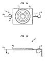
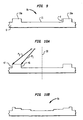
- FIGS. 1a and 1b are simplified schematic diagrams, plan view and side view, respectively, of an optical modulator/switch 1.
- the optical modulator/switch 1 includes a reflective zone plate 8 defined in or on a zone-plate support 6.
- the zone-plate support is mechanically connected to a support means 4.
- the optical modulator/switch 1 further includes a movement means 18 for rotating or tilting the reflective zone plate 8 away from an axis 30.
- the reflective zone plate 8 can be rotated in the direction 31 about the axis 30 or in the direction 32 away from the axis 30. Further description of the support means 4 and the movement means 18 are presented later in this specification in conjunction with several preferred embodiments of the optical modulator/switch.
- the reflective zone plate 8 behaves in a manner quite similar to a lens, focusing an incident optical signal. It accomplishes this result as follows. In the absence of the reflective zone plate 8, the amplitude of light reflected from a mirror decreases with total distance from the mirror due to the diverging light beam. If the mirror is divided into a series of concentric rings or zones, the amplitude of the reflected light is simply the sum of the contributions from each of the zones. Since the light from each zone travels a slightly different overall distance, each contribution arrives at a detection point with a different phase. This leads to interference effects.
- the reflective zone plate can be used to greatly enhance the total amplitude at a given distance from the plate, i.e., at a "focal point.”
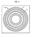
- the destructive contributions are removed by constructing a series of properly spaced non-reflecting rings, such as illustrated in FIG. 2.
- the reflective zone plate 8a shown in FIG. 2 is defined by four spaced, concentrically-disposed, circularly-shaped non-reflective regions 10. Reflective regions 11 are located between the non-reflective regions 10. The reflective regions 11 are located to achieve a net constructive interference at the location of the detector.
- a reflective zone plate 8 for use in the present invention will vary with the wavelength of the optical signal being reflected, the distance of the reflective zone plate from a wave guide that delivers the optical signal, and the distance between the reflective zone plate and a waveguide, detector or the like that receives the reflected optical signal.
- a reflective zone plate may include more or less than four non-reflective regions 10 as a function of the aforementioned factors.
- Other embodiments of reflective zone plates, and methods for calculating the required number, m, of regions or zones and the radius, R i , of the regions 10, are described later in this specification.
- a reflective zone plate can be formed as shown in FIG. 2, except that the non-reflective regions 10 of the alternate embodiment are placed where the reflective regions 11 of the plate of FIG. 2 are located.
- the reflected amplitude from the two embodiments are similar, except for a phase difference of 180°.
- the phase is not important in terms of modulator/switch performance. The operation of an optical modulator/switch 1 according to the present invention is described below.
- the reflective zone plate 8 is aligned with the axis 30 and is normal to an incident optical signal 23.
- a signal 24 reflected from the reflective zone plate 8 will be directed back along the same path as the incident optical signal 23 but in the opposite direction.
- the reflective zone plate 8 is tilted from the axis 30 by an angle, ⁇ , so that the incident optical signal 23 is no longer normal to the reflective zone plate 8.
- the optical signal 24 will be reflected from the reflective zone plate 8 such that the angle described by the incident signal and the reflected signal is 2 ⁇ .
- the reflective zone plate can be used to modulate an optical signal or function as an optical switch.
- FIGS. 5a - 5g illustrate using the optical modulator/switch 1 with various wave guiding arrangements.
- FIGS. 5a and 5b illustrate an arrangement 100a wherein the optical modulator/switch 1 is used as an optical modulator.
- the arrangement 100a comprises the optical modulator/switch 1 and a wave guide 25 used for carrying both an incident optical signal and a reflected optical signal.
- wave guide refers to optical fibers or any other medium suitable for supporting the propagation of an optical signal.
- FIGS. 5a and 5b show the reflective zone plate 8 spaced from the wave guide 25.
- the axis 30 is perpendicular to the waveguide 25.
- the optical modulator/switch 1 is shown in its "untilted” or “quiescent” state wherein the reflective zone plate 8 is aligned along the axis 30. In the quiescent state, the reflective zone plate 8 is perpendicular to the wave guide 25. In this state, the reflective zone plate 8 receives an incident optical signal 23 and delivers a reflected optical signal 24 back to the wave guide 25.
- the optical modulator/switch 1 is shown in the "tilted” or “biased” state wherein the reflective zone plate 8 is tilted by the angle, ⁇ , from the axis 30. In the biased state, the reflective zone plate 8 is not perpendicular to the wave guide 25.
- the optical signal 24 reflected from the reflective zone plate 8 follows a path that is displaced by an angle, 2 ⁇ , from the incident optical signal 23 and will not be received by the wave guide 25.
- FIGS. 5c and 5d illustrates a second arrangement 100b wherein the optical modulator/switch 1 is used, once again, as an optical modulator.
- the arrangement 100b comprises the optical modulator/switch 1 and two wave guides 25 and 26.
- one of the waveguides, such as the wave guide 25, delivers the incident optical signal 23 to the reflective zone plate 8 and the other wave guide 26 receives the reflected optical signal 24.
- FIGS. 5c and 5d show the reflective zone plate 8 spaced from the wave guides 25 and 26.
- the wave guides 25 and 26 are positioned so that when the optical modulator/switch is in the quiescent state, shown in FIG. 5c, the reflected optical signal 24 is directed along a first path to the wave guide 26. In the biased state, shown in FIG. 5d, the reflected optical signal 24 is deflected by an angle, 2 ⁇ , from the first path. So deflected, the optical signal 24 is not received by the wave guide 26.
- FIGS. 5e and 5f illustrate an arrangement 200a wherein the optical modulator/switch 1 is used as an optical switch.
- the arrangement 200a comprises the optical modulator/switch 1 and three wave guides 25, 26 and 27.
- FIGS. 5e and 5f show the reflective zone plate 8 spaced from the three wave guides.
- the wave guide 25 delivers an optical signal 23 to the reflective zone plate 8 and one of the wave guides 26 or 27 receives the reflected optical signal 24.
- the wave guides 25 and 26 are positioned so that when the optical modulator/switch 1 is in the quiescent state, shown in FIG. 5e, the reflected optical signal 24 is directed along a first path to the wave guide 26. In the biased state, shown in FIG. 5d, the reflected optical signal 24 is deflected by an angle, 2 ⁇ , from the first path. So deflected, the optical signal 24 follows a second path to be received by the wave guide 27.
- FIG. 5g shows an arrangement 200b comprising the optical modulator/switch 1, a wave guide 25 for delivering an optical signal 23 and four wave guides, 26 - 29, for receiving the reflected optical signal 24.
- ⁇ tilt angle
- the optical path of the reflected signal 24 can be varied.
- the reflected optical signal 24 can be directed to any one of the four waveguides 26- 29.
- optical modulator/switch 1 While some elements of one embodiment may be structurally identical to elements in other embodiments, all elements pertaining to a particular embodiment, with the exception of the reflective zone plate 8, will be designated by an alphabetic character distinguishing them from the elements of other embodiments, e.g., all elements of modulator/ switch 1a will be designated by an identifier "a”, as well as by a reference numeral, while those of the modulator 1b will be designated by an identifier "b".
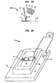
- FIG. 6a shows, in a perspective view, a preferred embodiment of a micromechanical optical modulator/switch 1a.
- the optical modulator/switch 1a includes a reflective zone plate 8 defined off-center in a flexible conductive zone-plate support 6a.
- the zone-plate support 6a is suspended above a conductive layer 2a by support structure 4a.
- contacts 14a and 16a are disposed on the conductive layer 2a and the zone-plate support 6a, respectively.
- the contacts 14a and 16a facilitate electrical connection to a controlled voltage source 18a.
- the zone-plate support 6a is referred to herein as a doubly-supported beam structure or configuration.
- FIGS. 6a and 6b show the optical modulator/switch 1a in a quiescent state, wherein the reflective zone plate 8 is perpendicular to an incident optical signal 23.
- the reflected optical signal 24 will return along the same path as the incident optical signal 23 but in the opposite direction.
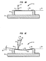
- FIG. 6c shows a cross-sectional view of the optical modulator/switch 1a in a biased state.
- the controlled-voltage source 18a applies a voltage across the zone-plate support 6a and conductive layer 2a.
- the applied voltage generates an electrostatic force that causes the zone-plate support 6a to move towards the conductive layer 2a.
- each end 41a, 42a of the zone-plate support 6a is attached to the support structure 4a.
- regions nearer the center 40a of the zone-plate support 6a deflect more, relative to the axis 30, than regions near the ends 41a, 42a of the zone-plate support 6a.
- the reflective zone plate 8 Since the reflective zone plate 8 is located off-center on the zone-plate support 6a, it will tilt downwardly toward the center 40a of the zone-plate support 6a. The reflective zone plate 8 will thus be displaced by an angle, ⁇ , relative to the axis 30, from its non-biased orientation. As such, an axis 33 normal to the reflective zone plate 8a will no longer be coincident with the incident optical signal 23. The reflected optical signal 24 will therefore not return to its source. The path of the reflected optical signal 24 will be displaced from the path of the incident optical signal 23 by 2 ⁇ .
- the zone-plate support 6a and the support structure 4a provide the function and structure indicated by the support means 4 of the optical modulator/switch 1 described earlier in this specification.
- the controlled-voltage source 18a in conjunction with the conductivity of the zone-plate support 6a and the conductive layer 2a, as well as the flexibility of the zone-plate support 6a provide the function and structure indicated by the movement means 18 of the modulator/switch 1.
- FIG. 7a shows, in a perspective view, a second preferred embodiment of a micromechanical optical modulator/switch 1b.
- the optical modulator/switch 1b includes a reflective zone plate 8 defined in a conductive zone-plate support 6b.
- a flexible member 7b depending from a side 41b of the zone-plate support 6b is attached to a support structure 4b.
- the support structure 4b in conjunction with the flexible member 7b, suspend the zone-plate support 6b above a conductive layer 2b.
- contacts 14b and 16c are disposed so that they are in electrical contact with the conductive layer 2b and the zone-plate support 6b, respectively.
- the contacts 14b and 16b facilitate electrical connection to a controlled voltage source 18b.
- the zone-plate support 6b in conjunction with the flexible member 7b are referred to herein as a cantilever structure or configuration.
- FIGS. 7a and 7b show the optical modulator/switch 1b in a quiescent state, wherein the reflective zone plate 8 is perpendicular to an incident optical signal 23.
- the reflected optical signal 24 will return along the same path as the incident optical signal 23 but in the opposite direction.
- FIG. 7c shows a cross-sectional view of the optical modulator/switch 1a in a biased state.
- the controlled-voltage source 18b applies a voltage across the zone-plate support 6b and conductive layer 2b.
- the resulting electrostatic force causes the zone-plate support 6b to move towards the conductive layer 2b.
- the end 41b of the zone-plate support 6b remains nearest the axis 30 while the end 42b of the zone-plate support deflects furthest from the axis 30.
- the reflective zone plate 8 tilts downwardly toward the end 42b.
- the reflective zone plate 8 will be thus be displaced by an angle, ⁇ , relative to the axis 30, from its non-biased orientation. As such, normal axis 33 will no longer be coincident with the incident optical signal 23. The reflected optical signal 24 will therefore not return to its source; its path will be displaced from the path of the incident optical signal 23 by 2 ⁇ .
- the zone-plate support 6b, flexible member 7b and the support structure 4b provide the function and structure indicated by the support means 4 of the optical modulator/switch 1 described earlier.
- the controlled-voltage source 18b and flexible member 7b in conjunction with the conductivity of the zone-plate support 6b and the conductive layer 2b, provide the function and structure indicated by the movement means 18 of the modulator/switch 1.
- FIG. 8a shows a third preferred embodiment of an optical modulator/switch 1c.
- the optical modulator/switch 1c includes a reflective zone plate 8 defined in an at least partially conductive zone-plate support 6c.
- Torsional members 7c and 7d, depending from sides 43c and 44c, respectively, of the zone-plate support 6c are attached to a support structure 4c.
- the support structure 4c in conjunction with the torsional members 7c and 7d, suspend the zone-plate support 6c above an at least partially conductive layer 2c.
- contacts 14c and 16c are disposed so that they are in electrical contact with the conductive layer 2c and the zone-plate support 6c, respectively.
- the contacts 14c and 16c facilitate electrical connection to a controlled voltage source 18c.
- torsional members 7c and 7d as a dividing line, only about one half of either the layer 2c or the zone-plate support 6c should be conductive.
- the zone-plate support 6c in conjunction with the torsional members 7c and 7d are referred to herein as a torsional structure or configuration.
- FIGS. 8a and 8b show the optical modulator/switch 1c in a quiescent state, wherein the reflective zone plate 8 is perpendicular to an incident optical signal 23.
- the reflected optical signal 24 will return along the same path as the incident optical signal 23 but in the opposite direction.
- FIG. 8c shows the optical modulatocr/switch 1c in a biased state.
- the controlled-voltage source 18c applies a voltage across the zone-plate support 6c and layer 2c.
- the applied voltage generates an electrostatic force that causes the conductive region of the zone-plate support 6c to move towards the conductive region of the layer 2c.
- the zone-plate support 6c rotates about the axis defined by the torsional members 7c and 7d so that one side of the zone-plate support is drawn towards the layer 2c.
- the reflective zone plate 8 tilts downwardly toward either the left or the right of the torsional members 7c and 7d, depending upon the location of the conductive regions.
- the reflective zone plate 8 will be thus be displaced by an angle, ⁇ , relative to the axis 30, from its non-biased orientation. As such, normal axis 33 will no longer be coincident with the incident optical signal 23.
- the reflected optical signal 24 will therefore not return to its source.
- the path of the reflected optical signal 24 will be displaced from the path of the incident optical signal 23 by 2 ⁇ .
- the zone-plate support 6c, torsional members 7c and 7d, and the support structure 4c provide the function and structure indicated by the support means 4 of the optical modulator/switch 1 described earlier in this specification.
- the controlled-voltage source 18c and torsional members 7c and 7d in conjunction with the conductive regions of the zone-plate support 6c and the layer 2c provide the function and structure indicated by the movement means 18 of the optical modulator/switch 1.
- an optical modulator/switch described above can be used in any of the arrangements 100a, 100b, 200a and 200b previously described.
- Surface and bulk micromachining techniques well-known to those skilled in the art can be used to form an optical modulator/switch embodying the present invention.
- elements such as the zone-plate support 6 and the conductive layer 2, which are indicated to be conductive or partially conductive, can either be intrinsically conductive, or rendered conductive by the deposition of suitably conductive materials or, as appropriate, by doping with appropriate species. Further details concerning the reflective zone plate 8 utilized in present invention are described below.
- FIG. 2 shows a reflective zone plate 8a defined by spaced, concentrically-disposed, circularly-shaped non-reflective regions 10 and circularly-shaped reflective regions 11 located therebetween.
- the non-reflective regions 10 can be transparent so that light passes through such regions and is absorbed by underlying layers, or they can be black.
- Reflective regions can be created by coating the smooth surface of a reflective zone plate 8a with a highly reflective material, such as aluminum or gold, in the appropriate regions 11.
- non-reflective and reflective regions it is within the capabilities of those skilled in the art to select an appropriate method, i.e., photolithographic, print, various deposition techniques, for applying materials to the zone-plate support 6 to form the non-reflective and reflective regions.
- an appropriate method i.e., photolithographic, print, various deposition techniques, for applying materials to the zone-plate support 6 to form the non-reflective and reflective regions.
- Other embodiments of non-reflective and reflective regions, and ways for forming such regions, that occur to those skilled in the art, can suitably be used.
- the surface of the reflective zone plate where the non-reflective regions would otherwise be located should be treated, as appropriate, to be reflective, and should be one-quarter of a wavelength higher, as indicated by the reference character, d, than the surface of the reflective regions 11.
- the roundtrip path length for light reflecting off such regions is decreased by one-half of a wavelength.
- the non-reflective regions 10 become phase-reversing reflecting regions 10a.
- the amplitude of an optical signal reflected from the reflective zone plate 8b is twice that of an optical signal reflected from reflective zone plate 8a.
- Surface or bulk micromachining techniques known to those skilled in the art can be used to form the ⁇ /4 steps in surface height.
- Suitable materials for the zone-plate support 6 include, without limitation, polysilicon, indium-tin-oxide (ITO) coated glass, silicon nitride, metal films and plastic.
- the path length, P 1 for light striking the inner edge 46 of a given zone is shorter than the path length, P 2 , for light striking the outer edge 47 of that zone, assuming an optical source located on the axis 50 through the center of the reflective zone plate 8a or 8b.
- This path length difference introduces phase shifts that result in an amount of destructive interference.
- the surface of each region is stepped upwardly as the radius of the region increases. While an infinite number of steps, i.e., a smooth, rising surface, would provide the best performance, fabrication would be difficult.
- step heights replace each pair of two level zones, although a two-step zone plate improves performance considerably relative to a flat surface.
- the step heights would typically repeat the sequence, 0, 1/8 ⁇ , 1/4 ⁇ and 3/8 ⁇ .
- the step height is ⁇ /(2b), with the first level always being zero.
- the zone radii of the reflective zone plate 8 are determined as follows. It is assumed that the source, S, of a Gaussian beam, i.e., the end of the wave guide delivering the optical signal, is a distance, d s , from the reflective zone plate and that the detection point, P, i.e., the end of the wave guide receiving the reflected optical signal, is a distance, d p , from the reflective zone plate. Both S and P are located on the symmetry axis of the reflective zone plate 8.
- R d s .
- the first zone then extends from the center of the reflective zone plate 8b out to R 1 , the second zone from R 1 to R 2 , and so forth.
- the solution to expression [1] is provided in Table 1.
- the zone radii, R m are expressed as a function of d s and m. Thus, m / ⁇ for a particular zone, m, is given at various values of d s / ⁇ , e.g., 100, 200 ... 500.
- the radii for a four-level reflective zone plate such as the reflective zone plate 8c shown in FIG. 10b are calculated as follows.
- the optical paths associated with neighboring zone boundaries differ by ⁇ /4.
- the first zone which has no extra phase shift, extends from the center of the reflective zone plate 8c out to S 1,1 .
- the second zone which has a phase shift of ⁇ /2, extends from S 1,1 to S 1,2 .
- the third zone has a phase shift of ⁇ and extends from S 1,2 to S 1,3 .
- the fourth zone with a phase shift of 3 ⁇ /2, extends from S 1,3 to S 1,4 .
- the sequence then repeats with the second zone, e.g., S 2,1 to S 2,4 .
- Tables 2a and 2b The solution to expression [2], which provides the zone radii S i,j for a four-level zone, is given in Tables 2a and 2b in terms of the optical wavelength, ⁇ .
- Table 2a provides the zone radii for zones 1 - 5, i.e, S 1,1 - S 5,4
- Table 2b provides the zone radii for zones 6 - 9.
- the zone radii, S ij are expressed as a function of d s , i and j.
- S ij / ⁇ for a particular zone, i, and step, j is given at various values of d s / ⁇ , e.g., 100, 200 ... 500.
- the "starred" radius in each column locates the largest effective zone radius for that value of d s / ⁇ .
- expression [2] can be used to calculate the zone radii for a reflective zone plate having a number, b, of steps or levels other than 4 by setting "b" in expression [2] equal to the other number of steps.
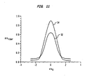
- FIG. 11 shows the calculated Gaussian profile of a four-level reflective zone plate, identified by the reference numeral 54, and the profile of a two-level reflective zone plate, identified by the reference numeral 52.
- the profile shows the relative amplitude, 52 and 54, of the reflected signal as a function of the relative radial distance from center of the optical signal.
- the relative amplitude is defined as the amplitude of the reflected signal at the detector (point P), i.e., at the end of the receiving wave guide, divided by the amplitude of the incident optical signal at the source (point S), i.e., at the end of the delivering wave guide.
- the relative radial distance is defined as the lateral distance from the center of the optical signal at point P, divided by the radius of the optical signal at point S.
- FIG. 11 shows that, on center, the optical signal reflected from a two-level reflective zone plate has an amplitude that is about 60 percent of the initial amplitude, for a signal loss of about 4 dB.
- the signal reflected from the four-level reflective zone plate has an amplitude that is about 90 percent of the initial amplitude, for a signal loss of about 1 dB.
- the optical signal reflected from the reflective zone plate 8 must be captured by the aperture of a wave guide, typically an optical fiber. As such, it is important that the reflected signal has an appropriate beam width, i.e., spot size, at the end of the receiving fiber. Spot size can be adjusted by varying the distance between the source, i.e., the end of the fiber delivering the optical signal, and the reflective zone plate 8.
- FIGS. 12a - 12c show the relative amplitude of the reflected optical signal as a function of the relative radial distance, ⁇ / w o , for several values of d s / ⁇ . For FIGS.
- the relative radial distance ⁇ / w o is defined as the radial distance from the center of the receiving fiber divided by the width of the optical signal at the end of the delivering fiber.
- d p / ⁇ 200.
- FIGS. 12a - 12c show that as the distance between the source fiber and the reflective zone plate 8 increases, the profile narrows. As such, a greater portion of the energy is captured within a smaller radius at greater source to plate distances.
- the spacing between the end of the source wave guide and the reflective zone plate can be adjusted for the aperature of the receiving wave guide.
- the reflected optical beam must be directed toward one or more wave guides.
- the reflective zone plate 8 must be tilted to a particular angle, ⁇ .
- the tilt of the reflective zone plate 8 corresponds to a particular deflection of the zone-plate support 6.
- the amount that the zone-plate support deflects is controlled by the applied voltage, V.
- the voltage, V, required for a particular deflection of the zone-plate support can be determined by routine experimentation. Alternatively, the voltage, V, calculated according to the following methods.
- the voltage, V, required for a particular amount of deflection of the zone-plate support 6a having a doubly supported beam configuration can be determined as follows, referring to FIGS. 13 and 14.
- Z x ⁇ V Z mp V ⁇ cos ⁇ ⁇ / L
- Z mp is the displacement of the zone-plate support 6a at the midpoint
- L is the length of the zone-plate support 6a.
- the tilt angle, ⁇ , of the zone plate 8a can be determined by geometry. Knowing the tilt angle and the length of the zone-plate support 6a, the required relative displacement, Z mp /t eff , of the zone plate support 6a can be determined. The corresponding value of U can be read from FIG. 14. This value of U and expression [5] can then be used to determine the voltage, V, to achieve the desired tilt angle ⁇ .
- E Young's modulus
- I the moment of inertia and the other variables are as previously defined.
- the tilt angle and voltage requirements can be determined in a manner similar to that described for the doubly-supported beam configuration.
Landscapes
- Physics & Mathematics (AREA)
- General Physics & Mathematics (AREA)
- Optics & Photonics (AREA)
- Mechanical Light Control Or Optical Switches (AREA)
- Micromachines (AREA)
Description
- The present invention relates to optical modulators/switches, to methods for modulating an optical signal, and to methods for switching an optical signal.
- There is increasing interest in developing inexpensive optical modulators and switches. A number of structures for optical modulators have been proposed. Most utilize a variable air gap defined by two layers of material, at least one of which layers is movable. Varying the air gap by moving one of the layers changes an optical property of the device, typically the reflectivity. Thus, in one state, the modulator is highly reflective to an incident optical signal, and in another state, the modulator has a very low reflectivity to the incident optical signal. This difference in reflectivity is used to modulate the optical signal. Such modulators are usually activated by applying a voltage across the two layers generating an electrostatic force that causes the movable layer to move towards the other layer.
- There are a number of drawbacks associated with modulators having the aforementioned structure. For example, a particular value of the voltage, e.g., 37.4 volts, may be required for moving the movable layer a specified distance to achieve a maximum change in optical properties between the "voltage-off" and the "voltage-on" state. As the modulator ages, the particular value may change. To the extent the driven voltage is not suitably adjusted, modulator performance is degraded. Furthermore, the underlying optical principles of the device may place constraints on the thickness or other characteristics of the layers. Such constraints limit materials selection and complicate fabrication. Also, such modulators are typically used with only a single optical fiber, limiting the potential usefulness of these devices.
- Thus, there is a need for an optical modulator that avoids these drawbacks of the prior art.
-
EP-A-0 420 468 discloses a movable concave mirror configured to switch an optical signal between a number of waveguides. - An optical modulator/switch and methods of modulation and switching according to the invention are set out in the independent claims.
- The distance between the reflective zone plate and the focal location is preferably in the range from about 100 to about 500 times the wavelength of the incident optical signal.
- The regions that prevent negative contributions to the amplitude of the reflected signal from reaching the focal location may be such as not to reflect negative contributions. Alternatively they may be adapted to change the phase of the reflected optical signal by about 180°.
- The optical modulator/switch may further comprise a waveguide having a first end positioned at the focal location.
- In one form, the zone-plate support is flexible and has a doubly-supported beam configuration. In another form the zone-plate support has a cantilever configuration, and in yet another form the zone-plate support has a torsional configuration.
- Each region of the first and second plurality of regions may be further comprised of sections, each section within a region differing in height from an adjacent section in the region by the same amount.
- An optical modulator/switch is disclosed. The optical modulator/switch includes a reflective zone plate for reflecting an incident optical signal. The optical modulator/switch further includes a means for rotating or tilting the reflective zone plate from an initial orientation, typically normal to an incident optical signal, to at least one other orientation.
- The reflective zone plate functions as a lens, receiving an incoming optical signal and focusing a reflected signal. The zone plate alters the phase of, or removes, contributions to the optical signal which result in destructive interference upon reflection. The resulting reflected optical signal has a much higher central intensity than if the signal was reflected from a mirror or other reflective surface.
- By tilting the reflective zone plate away from its initial orientation, the direction of the reflected optical signal can be altered. In one embodiment of a modulator/switch according to the present invention, the reflective zone plate is rapidly tilted between its initial orientation when the modulator/switch is in a quiescent state, and a second orientation ("the biased state of the modulator/switch") in response to a voltage signal from a controlled voltage source. In the quiescent state, the reflected signal is in optical communication with a wave guide; in the biased state, the path of the reflected signal is altered so that the optical signal is no longer in optical communication with the wave guide. In this manner, an optical signal can be modulated with very high contrast between the quiescent and biased states. Moreover, a modulator/switch according to the present invention does not have to be operated at a specific voltage to achieve maximum contrast between the two states. Rather, as long the voltage is sufficient to tilt the reflective zone plate enough to ensure that, in the biased state, the optical signal is not captured by the wave guide, maximum contrast is achieved. Furthermore, since, in preferred embodiments, the optical signal is reflecting from a high reflectivity coating, there are relatively few limitations regarding suitable support materials for the reflective zone plate.
- In other embodiments, the reflective zone plate can be tilted to a plurality of orientations, each of which orientations result in different optical paths for a reflected optical signal. In each orientation, the reflective zone plate is in optical communication with a different wave guide. Thus, in response to a voltage signal from a controlled voltage source, an incident optical signal can be switched to any one of a plurality of wave guides.
- Further features of the invention will become more apparent from the following detailed description of specific embodiments thereof when read in conjunction with the accompanying drawings in which:
- FIG. 1a is a plan view of a conceptual schematic of an optical modulator/switch embodying the present invention;
- FIG. 1b is a side-view of the modulator/switch of FIG. 1a ;
- FIG. 2 is an exemplary embodiment of a reflective zone plate;
- FIG. 3 is a partial view of a modulator/switch embodying the present invention wherein the reflective zone plate is coincident with an axis perpendicular to an incident optical signal;
- FIG. 4 shows the modulator/switch of FIG. 3 wherein the reflective zone plate is tilted relative to the axis;
- FIG. 5a shows an arrangement wherein a modulator/switch embodying the present invention is being used in conjunction with one wave guide to modulate an optical signal, wherein the reflective zone plate of the modulator/switch is coincident with an axis perpendicular to the incident optical signal;
- FIG. 5b shows the arrangement of FIG. 5a wherein the reflective zone plate is tilted relative to the axis;
- FIG. 5c shows an arrangement wherein a modulator/switch embodying the present invention is being used in conjunction with two wave guides to modulate an optical signal, the modulator/switch being shown in the quiescent state;
- FIG. 5d shows the arrangement of FIG. 5c in the biased state;
- FIG. 5e shows an arrangement wherein a modulator/switch embodying the present invention is being used in conjunction with three wave guides to function as a switch, wherein the modulator/switch is shown in the quiescent state;
- FIG. 5f shows the arrangement of FIG. 5e wherein the modulator/switch is shown in the biased state;
- FIG. 5g shows an arrangement wherein a modulator/switch embodying the present invention is being used in conjunction with five wave guides to function as a switch;
- FIG. 6a is a perspective view of a first preferred embodiment of an optical modulator/ switch wherein the zone-plate support is configured as a doubly-supported beam;
- FIG. 6b shows the optical modulator/switch of FIG. 6a in the quiescent state;
- FIG. 6c shows the optical modulator/switch of FIG. 6a in the biased state;
- FIG. 7a is a perspective view of a second preferred embodiment of an optical modulator/ switch wherein the zone-plate support is configured as a cantilevered structure;
- FIG. 7b shows the optical modulator/switch of FIG. 7a in the quiescent state;
- FIG. 7c shows the optical modulator/switch of FIG. 7a in the biased state;
- FIG. 8a is a perspective view of a third preferred embodiment of an optical modulator/ switch wherein the zone-plate support is configured as a torsional structure;
- FIG. 8b shows the optical modulator/switch of FIG. 8a in the quiescent state;
- FIG. 8c shows the optical modulator/switch of FIG. 8a in the biased state;
- FIG. 9 illustrates a first preferred embodiment of a reflective zone plate;
- FIG. 10a demonstrates optical path length differences between sections of a given zone or region;
- FIG. 10b shows a second preferred embodiment of a reflective zone plate;
- FIG. 11 shows the relative amplitude of a reflected signal for a four-level reflective zone plate and a two-level reflective zone plate as a function of the relative radial distance from center of the optical signal;
- FIGS. 12a - 12c show the relative amplitude of a reflected optical signal as a function of the relative radial distance for ds/λ = 320, 250 and 200, respectively;
- FIG. 13 is an illustration of a doubly-suspended beam; and
- FIG. 14 shows the universal curve Zmp / teff as a function of U, which is useful for determining drive voltage requirements for a given membrane displacement.
- FIGS. 1a and 1b are simplified schematic diagrams, plan view and side view, respectively, of an optical modulator/switch 1. The optical modulator/switch 1 includes a
reflective zone plate 8 defined in or on a zone-plate support 6. The zone-plate support is mechanically connected to a support means 4. The optical modulator/switch 1 further includes a movement means 18 for rotating or tilting thereflective zone plate 8 away from anaxis 30. Depending upon the specific embodiment of the modulator/switch 1, several of which are described later in this specification, thereflective zone plate 8 can be rotated in thedirection 31 about theaxis 30 or in thedirection 32 away from theaxis 30. Further description of the support means 4 and the movement means 18 are presented later in this specification in conjunction with several preferred embodiments of the optical modulator/switch. - The
reflective zone plate 8 behaves in a manner quite similar to a lens, focusing an incident optical signal. It accomplishes this result as follows. In the absence of thereflective zone plate 8, the amplitude of light reflected from a mirror decreases with total distance from the mirror due to the diverging light beam. If the mirror is divided into a series of concentric rings or zones, the amplitude of the reflected light is simply the sum of the contributions from each of the zones. Since the light from each zone travels a slightly different overall distance, each contribution arrives at a detection point with a different phase. This leads to interference effects. By removing those zones that lead to destructive interference, the reflective zone plate can be used to greatly enhance the total amplitude at a given distance from the plate, i.e., at a "focal point." In one embodiment, the destructive contributions are removed by constructing a series of properly spaced non-reflecting rings, such as illustrated in FIG. 2. - The
reflective zone plate 8a shown in FIG. 2 is defined by four spaced, concentrically-disposed, circularly-shapednon-reflective regions 10.Reflective regions 11 are located between thenon-reflective regions 10. Thereflective regions 11 are located to achieve a net constructive interference at the location of the detector. - It should be understood that the configuration of a
reflective zone plate 8 for use in the present invention will vary with the wavelength of the optical signal being reflected, the distance of the reflective zone plate from a wave guide that delivers the optical signal, and the distance between the reflective zone plate and a waveguide, detector or the like that receives the reflected optical signal. Thus, in other embodiments, a reflective zone plate may include more or less than fournon-reflective regions 10 as a function of the aforementioned factors. Other embodiments of reflective zone plates, and methods for calculating the required number, m, of regions or zones and the radius, Ri, of theregions 10, are described later in this specification. - Moreover, it will be appreciated that in an alternate embodiment, a reflective zone plate can be formed as shown in FIG. 2, except that the
non-reflective regions 10 of the alternate embodiment are placed where thereflective regions 11 of the plate of FIG. 2 are located. The reflected amplitude from the two embodiments are similar, except for a phase difference of 180°. The phase is not important in terms of modulator/switch performance. The operation of an optical modulator/switch 1 according to the present invention is described below. - In FIG. 3, the
reflective zone plate 8 is aligned with theaxis 30 and is normal to an incidentoptical signal 23. Thus, asignal 24 reflected from thereflective zone plate 8 will be directed back along the same path as the incidentoptical signal 23 but in the opposite direction. In FIG. 4, thereflective zone plate 8 is tilted from theaxis 30 by an angle, β, so that the incidentoptical signal 23 is no longer normal to thereflective zone plate 8. As such, theoptical signal 24 will be reflected from thereflective zone plate 8 such that the angle described by the incident signal and the reflected signal is 2β. As described below, by rapidly tilting thereflective zone plate 8 between those two orientations in response to a control signal, the reflective zone plate can be used to modulate an optical signal or function as an optical switch. FIGS. 5a - 5g illustrate using the optical modulator/switch 1 with various wave guiding arrangements. - FIGS. 5a and 5b illustrate an
arrangement 100a wherein the optical modulator/switch 1 is used as an optical modulator. Thearrangement 100a comprises the optical modulator/switch 1 and awave guide 25 used for carrying both an incident optical signal and a reflected optical signal. As used herein, the term "wave guide" refers to optical fibers or any other medium suitable for supporting the propagation of an optical signal. FIGS. 5a and 5b show thereflective zone plate 8 spaced from thewave guide 25. Theaxis 30 is perpendicular to thewaveguide 25. - In FIG. 5a, the optical modulator/switch 1 is shown in its "untilted" or "quiescent" state wherein the
reflective zone plate 8 is aligned along theaxis 30. In the quiescent state, thereflective zone plate 8 is perpendicular to thewave guide 25. In this state, thereflective zone plate 8 receives an incidentoptical signal 23 and delivers a reflectedoptical signal 24 back to thewave guide 25. In FIG. 5b, the optical modulator/switch 1 is shown in the "tilted" or "biased" state wherein thereflective zone plate 8 is tilted by the angle, β, from theaxis 30. In the biased state, thereflective zone plate 8 is not perpendicular to thewave guide 25. Thus, in the biased state, theoptical signal 24 reflected from thereflective zone plate 8 follows a path that is displaced by an angle, 2β, from the incidentoptical signal 23 and will not be received by thewave guide 25. - FIGS. 5c and 5d illustrates a
second arrangement 100b wherein the optical modulator/switch 1 is used, once again, as an optical modulator. Thearrangement 100b comprises the optical modulator/switch 1 and two wave guides 25 and 26. In the arrangment 100b, one of the waveguides, such as thewave guide 25, delivers the incidentoptical signal 23 to thereflective zone plate 8 and the other wave guide 26 receives the reflectedoptical signal 24. FIGS. 5c and 5d show thereflective zone plate 8 spaced from the wave guides 25 and 26. The wave guides 25 and 26 are positioned so that when the optical modulator/switch is in the quiescent state, shown in FIG. 5c, the reflectedoptical signal 24 is directed along a first path to thewave guide 26. In the biased state, shown in FIG. 5d, the reflectedoptical signal 24 is deflected by an angle, 2β, from the first path. So deflected, theoptical signal 24 is not received by thewave guide 26. - FIGS. 5e and 5f illustrate an
arrangement 200a wherein the optical modulator/switch 1 is used as an optical switch. Thearrangement 200a comprises the optical modulator/switch 1 and three wave guides 25, 26 and 27. FIGS. 5e and 5f show thereflective zone plate 8 spaced from the three wave guides. Thewave guide 25 delivers anoptical signal 23 to thereflective zone plate 8 and one of the wave guides 26 or 27 receives the reflectedoptical signal 24. The wave guides 25 and 26 are positioned so that when the optical modulator/switch 1 is in the quiescent state, shown in FIG. 5e, the reflectedoptical signal 24 is directed along a first path to thewave guide 26. In the biased state, shown in FIG. 5d, the reflectedoptical signal 24 is deflected by an angle, 2β, from the first path. So deflected, theoptical signal 24 follows a second path to be received by thewave guide 27. - It will be appreciated that in other embodiments, such as, for example, an embodiment shown in FIG. 5g, further wave guides can be used for receiving the reflected
optical signal 24. FIG. 5g shows an arrangement 200b comprising the optical modulator/switch 1, awave guide 25 for delivering anoptical signal 23 and four wave guides, 26 - 29, for receiving the reflectedoptical signal 24. By varying the tilt angle, β, of thereflective zone plate 8 relative to theaxis 30, the optical path of the reflectedsignal 24 can be varied. Thus, by causing thereflective zone plate 8 to appropriately tilt, the reflectedoptical signal 24 can be directed to any one of the four waveguides 26- 29. - Guidelines concerning the spacing between the
reflective zone plate 8 and the wave guides for arrangements such as those described above will be provided later in this specification. - Having described the general features of the optical modulator/switch 1, its operation and exemplary uses, three specific embodiments of an optical modulator/switch embodying the present invention, and methods for making them, will be described below. While some elements of one embodiment may be structurally identical to elements in other embodiments, all elements pertaining to a particular embodiment, with the exception of the
reflective zone plate 8, will be designated by an alphabetic character distinguishing them from the elements of other embodiments, e.g., all elements of modulator/switch 1a will be designated by an identifier "a", as well as by a reference numeral, while those of themodulator 1b will be designated by an identifier "b". - FIG. 6a shows, in a perspective view, a preferred embodiment of a micromechanical optical modulator/
switch 1a. The optical modulator/switch 1a includes areflective zone plate 8 defined off-center in a flexible conductive zone-plate support 6a. The zone-plate support 6a is suspended above aconductive layer 2a bysupport structure 4a. In a preferred embodiment,contacts conductive layer 2a and the zone-plate support 6a, respectively. Thecontacts voltage source 18a. The zone-plate support 6a is referred to herein as a doubly-supported beam structure or configuration. - Regarding operation, FIGS. 6a and 6b show the optical modulator/
switch 1a in a quiescent state, wherein thereflective zone plate 8 is perpendicular to an incidentoptical signal 23. The reflectedoptical signal 24 will return along the same path as the incidentoptical signal 23 but in the opposite direction. - FIG. 6c shows a cross-sectional view of the optical modulator/
switch 1a in a biased state. In response to a control signal, the controlled-voltage source 18a applies a voltage across the zone-plate support 6a andconductive layer 2a. The applied voltage generates an electrostatic force that causes the zone-plate support 6a to move towards theconductive layer 2a. In the optical modulator/switch 1a, eachend plate support 6a is attached to thesupport structure 4a. Thus, when the optical modulator/switch 1a is under bias, regions nearer thecenter 40a of the zone-plate support 6a deflect more, relative to theaxis 30, than regions near theends plate support 6a. Since thereflective zone plate 8 is located off-center on the zone-plate support 6a, it will tilt downwardly toward thecenter 40a of the zone-plate support 6a. Thereflective zone plate 8 will thus be displaced by an angle, β, relative to theaxis 30, from its non-biased orientation. As such, anaxis 33 normal to thereflective zone plate 8a will no longer be coincident with the incidentoptical signal 23. The reflectedoptical signal 24 will therefore not return to its source. The path of the reflectedoptical signal 24 will be displaced from the path of the incidentoptical signal 23 by 2β. - In the optical modulator/
switch 1a, the zone-plate support 6a and thesupport structure 4a provide the function and structure indicated by the support means 4 of the optical modulator/switch 1 described earlier in this specification. The controlled-voltage source 18a in conjunction with the conductivity of the zone-plate support 6a and theconductive layer 2a, as well as the flexibility of the zone-plate support 6a provide the function and structure indicated by the movement means 18 of the modulator/switch 1. - FIG. 7a shows, in a perspective view, a second preferred embodiment of a micromechanical optical modulator/
switch 1b. The optical modulator/switch 1b includes areflective zone plate 8 defined in a conductive zone-plate support 6b. Aflexible member 7b depending from aside 41b of the zone-plate support 6b is attached to asupport structure 4b. Thesupport structure 4b, in conjunction with theflexible member 7b, suspend the zone-plate support 6b above aconductive layer 2b. In a preferred embodiment,contacts conductive layer 2b and the zone-plate support 6b, respectively. Thecontacts voltage source 18b. The zone-plate support 6b in conjunction with theflexible member 7b are referred to herein as a cantilever structure or configuration. - Regarding operation, FIGS. 7a and 7b show the optical modulator/
switch 1b in a quiescent state, wherein thereflective zone plate 8 is perpendicular to an incidentoptical signal 23. The reflectedoptical signal 24 will return along the same path as the incidentoptical signal 23 but in the opposite direction. - FIG. 7c shows a cross-sectional view of the optical modulator/
switch 1a in a biased state. In response to a control signal, the controlled-voltage source 18b applies a voltage across the zone-plate support 6b andconductive layer 2b. The resulting electrostatic force causes the zone-plate support 6b to move towards theconductive layer 2b. In the cantilever configuration of the optical modulator/switch 1b, theend 41b of the zone-plate support 6b remains nearest theaxis 30 while theend 42b of the zone-plate support deflects furthest from theaxis 30. Thus, when the optical modulator/switch 1b is under bias, thereflective zone plate 8 tilts downwardly toward theend 42b. Thereflective zone plate 8 will be thus be displaced by an angle, β, relative to theaxis 30, from its non-biased orientation. As such,normal axis 33 will no longer be coincident with the incidentoptical signal 23. The reflectedoptical signal 24 will therefore not return to its source; its path will be displaced from the path of the incidentoptical signal 23 by 2β. - In the modulator/
switch 1b, the zone-plate support 6b,flexible member 7b and thesupport structure 4b provide the function and structure indicated by the support means 4 of the optical modulator/switch 1 described earlier. The controlled-voltage source 18b andflexible member 7b, in conjunction with the conductivity of the zone-plate support 6b and theconductive layer 2b, provide the function and structure indicated by the movement means 18 of the modulator/switch 1. - FIG. 8a shows a third preferred embodiment of an optical modulator/
switch 1c. The optical modulator/switch 1c includes areflective zone plate 8 defined in an at least partially conductive zone-plate support 6c. Torsionalmembers sides 43c and 44c, respectively, of the zone-plate support 6c are attached to asupport structure 4c. Thesupport structure 4c, in conjunction with thetorsional members plate support 6c above an at least partiallyconductive layer 2c. In a preferred embodiment,contacts conductive layer 2c and the zone-plate support 6c, respectively. Thecontacts voltage source 18c. Using thetorsional members layer 2c or the zone-plate support 6c should be conductive. The zone-plate support 6c in conjunction with thetorsional members - Regarding operation, FIGS. 8a and 8b show the optical modulator/
switch 1c in a quiescent state, wherein thereflective zone plate 8 is perpendicular to an incidentoptical signal 23. The reflectedoptical signal 24 will return along the same path as the incidentoptical signal 23 but in the opposite direction. - FIG. 8c shows the optical modulatocr/
switch 1c in a biased state. In response to a control signal, the controlled-voltage source 18c applies a voltage across the zone-plate support 6c andlayer 2c. The applied voltage generates an electrostatic force that causes the conductive region of the zone-plate support 6c to move towards the conductive region of thelayer 2c. In the torsional configuration of the optical modulator/switch 1c, the zone-plate support 6c rotates about the axis defined by thetorsional members layer 2c. Thus, when the optical modulator/switch 1c is under bias, thereflective zone plate 8 tilts downwardly toward either the left or the right of thetorsional members reflective zone plate 8 will be thus be displaced by an angle, β, relative to theaxis 30, from its non-biased orientation. As such,normal axis 33 will no longer be coincident with the incidentoptical signal 23. The reflectedoptical signal 24 will therefore not return to its source. The path of the reflectedoptical signal 24 will be displaced from the path of the incidentoptical signal 23 by 2β. - In the optical modulator/
switch 1c, the zone-plate support 6c,torsional members support structure 4c provide the function and structure indicated by the support means 4 of the optical modulator/switch 1 described earlier in this specification. The controlled-voltage source 18c andtorsional members plate support 6c and thelayer 2c provide the function and structure indicated by the movement means 18 of the optical modulator/switch 1. - The various embodiments of an optical modulator/switch described above can be used in any of the
arrangements plate support 6 and theconductive layer 2, which are indicated to be conductive or partially conductive, can either be intrinsically conductive, or rendered conductive by the deposition of suitably conductive materials or, as appropriate, by doping with appropriate species. Further details concerning thereflective zone plate 8 utilized in present invention are described below. - As previously described, a
reflective zone plate 8 utilized in the present invention can be configured as illustrated in FIG. 2. FIG. 2 shows areflective zone plate 8a defined by spaced, concentrically-disposed, circularly-shapednon-reflective regions 10 and circularly-shapedreflective regions 11 located therebetween. Those skilled in the art will know many ways for creating the non-reflective and reflective regions. For example, thenon-reflective regions 10 can be transparent so that light passes through such regions and is absorbed by underlying layers, or they can be black. Reflective regions can be created by coating the smooth surface of areflective zone plate 8a with a highly reflective material, such as aluminum or gold, in theappropriate regions 11. It is within the capabilities of those skilled in the art to select an appropriate method, i.e., photolithographic, print, various deposition techniques, for applying materials to the zone-plate support 6 to form the non-reflective and reflective regions. Other embodiments of non-reflective and reflective regions, and ways for forming such regions, that occur to those skilled in the art, can suitably be used. - For optical modulators/switches using the
reflective zone plate 8a, half of the incident optical signal is lost in thenon-reflective regions 10. It will be appreciated by those skilled in the art that by increasing or decreasing the path length of the "out-of-phase" contributions to the optical signal by one-half of a wavelength, such contributions will be brought in-phase with the rest of the optical signal. In a preferred embodiment of areflective zone plate 8b, shown in FIG. 9, the surface of the reflective zone plate where the non-reflective regions would otherwise be located should be treated, as appropriate, to be reflective, and should be one-quarter of a wavelength higher, as indicated by the reference character, d, than the surface of thereflective regions 11. The roundtrip path length for light reflecting off such regions is decreased by one-half of a wavelength. Thus, thenon-reflective regions 10 become phase-reversing reflectingregions 10a. The amplitude of an optical signal reflected from thereflective zone plate 8b is twice that of an optical signal reflected fromreflective zone plate 8a. Surface or bulk micromachining techniques known to those skilled in the art can be used to form the λ/4 steps in surface height. - There are tyically fewer limitations on the materials choice for the various elements of a modulator/switch embodying the present invention than for typical modulators. Surface treatments can be used to form the desired regions, e.g., non-reflective, reflective and phase-reversing. Suitable materials for the zone-
plate support 6 include, without limitation, polysilicon, indium-tin-oxide (ITO) coated glass, silicon nitride, metal films and plastic. - Referring to FIG. 10a, the path length, P1, for light striking the
inner edge 46 of a given zone is shorter than the path length, P2, for light striking theouter edge 47 of that zone, assuming an optical source located on theaxis 50 through the center of thereflective zone plate reflective zone plate 8c shown in FIG. 10b, the surface of each region is stepped upwardly as the radius of the region increases. While an infinite number of steps, i.e., a smooth, rising surface, would provide the best performance, fabrication would be difficult. Preferably, at least four "steps" replace each pair of two level zones, although a two-step zone plate improves performance considerably relative to a flat surface. For a four level plate, the step heights would typically repeat the sequence, 0, 1/8λ, 1/4λ and 3/8λ. For a zone plate having a number, b, of steps or levels, the step height is λ/(2b), with the first level always being zero. - The zone radii of the
reflective zone plate 8 are determined as follows. It is assumed that the source, S, of a Gaussian beam, i.e., the end of the wave guide delivering the optical signal, is a distance, ds, from the reflective zone plate and that the detection point, P, i.e., the end of the wave guide receiving the reflected optical signal, is a distance, dp, from the reflective zone plate. Both S and P are located on the symmetry axis of thereflective zone plate 8. - For a
reflective zone plate 8 having two regions, such as thereflective zone plate 8a, including one having two steps or levels, such as the phase reversingreflective zone plate 8b, the zone radii are determined by the relation:
where: r = (Rm 2 + dp 2)0.5 and m = integer and where R is the radius of curvature of the phase front a distance, ds, from the source S. When ds is large compared to λ, then R= ds. - The first zone then extends from the center of the
reflective zone plate 8b out to R1, the second zone from R1 to R2, and so forth. The solution to expression [1] is provided in Table 1. The zone radii, Rm, are expressed in terms of λ, the wavelength of the incident optical signal. Table 1 is based on the condition ds = dp. In other words, the wave guide delivering the optical signal and the wave guide receiving the reflected optical signal are the same distance from the reflective zone plate. The zone radii, Rm, are expressed as a function of ds and m. Thus, m/λ for a particular zone, m, is given at various values of ds/λ, e.g., 100, 200 ... 500. - About 99 percent of the energy of the optical signal is contained within a radius that is 1.5 times the radius of the optical beam at any given distance from the optical source, i.e., the end of the wave guide. Thus, zones having radii exceeding 1.5 times the beam radius will have negligible impact on the intensity of the reflected optical signal. The "starred" radius in each column locates the largest effective zone radius, i.e., the largest zone radius that is less than 1.5 times the beam radius, for that value of ds/λ. For example, if ds/λ = 100, no more than 3 zones are required.
Table I Zone Radii Rm for a Two-Level Reflective Zone Plate Rm/λ m ds/λ = 100 ds/λ=200 ds/λ=300 ds/ λ = 400 ds/ λ = 500 1 7.38 10.11 12.31 14.18 15.84 2 10.44 14.31 17.41 20.06 22.40 3 **12.79** 17.53 21.33 24.57 27.44 4 20.24 24.63 28.37 31.69 5 22.64 27.54 31.73 35.43 6 **24.80** 30.17 34.76 38.81 7 32.60 37.54 41.93 8 34.85 40.14 44.83 9 **36.97** 42.58 47.55 10 44.89 50.12 11 47.08 52.57 12 49.18 54.91 13 **51.19** 57.16 14 59.32 15 61.41 16 **63.43** - The radii for a four-level reflective zone plate such as the
reflective zone plate 8c shown in FIG. 10b are calculated as follows. The optical paths associated with neighboring zone boundaries differ by λ/4. The radii of the four-level reflective zone plate is denoted Si,j, and is given by:
where: i is the zone number and j is the step level, i.e., j = 1,2,3,4 and b is the number of steps, e.g., 4 in the present example. - The first zone, which has no extra phase shift, extends from the center of the
reflective zone plate 8c out to S1,1. The second zone, which has a phase shift of π/2, extends from S1,1 to S1,2. The third zone has a phase shift of π and extends from S1,2 to S1,3. And the fourth zone, with a phase shift of 3π/2, extends from S1,3 to S1,4. The sequence then repeats with the second zone, e.g., S2,1 to S2,4. - The solution to expression [2], which provides the zone radii Si,j for a four-level zone, is given in Tables 2a and 2b in terms of the optical wavelength, λ. Table 2a provides the zone radii for zones 1 - 5, i.e, S1,1 - S5,4 , and Table 2b provides the zone radii for zones 6 - 9. Tables 2a and 2b are based on the condition ds = dp. The zone radii, Sij , are expressed as a function of ds, i and j. Thus, Sij/λ for a particular zone, i, and step, j, is given at various values of ds/λ, e.g., 100, 200 ... 500. The "starred" radius in each column locates the largest effective zone radius for that value of ds/λ.
- It should be appreciated that expression [2] can be used to calculate the zone radii for a reflective zone plate having a number, b, of steps or levels other than 4 by setting "b" in expression [2] equal to the other number of steps.
Table 2a Zone Radii Sij for a Four-Level Reflective Zone Plate Zones 1-5 Si.j/λ i j ds/λ=100 ds/λ = 200 ds/λ = 300 ds/λ = 400 ds/λ = 500 1 1 0 0 0 0 0 1 2 5.22 7.16 8.71 10.03 11.20 1 3 7.38 10.12 12.31 14.18 15.84 1 4 9.04 12.39 15.08 17.37 19.40 2 1 10.44 14.31 17.42 20.06 22.41 2 2 11.67 16.00 19.47 22.43 25.05 2 3 12.79 17.53 21.33 24.57 27.44 2 4 **13.82** 18.94 23.04 26.54 29.64 3 1 20.25 24.64 28.38 31.69 3 2 21.48 26.13 30.10 33.61 3 3 22.64 27.55 31.73 35.43 3 4 23.75 28.89 33.28 37.16 4 1 24.81 30.18 34.76 38.82 4 2 **25.82** 31.41 36.18 40.41 4 3 32.60 37.55 41.93 4 4 33.75 38.87 43.40 5 1 34.85 40.15 44.83 5 2 35.93 41.38 46.21 5 3 36.97 42.58 47.55 5 4 **37.99** 43.75 48.86 Table 2b Zone Radii Sij for a Four-Level Reflective Zone Plate Zones 6-9 Si.j/λ i j ds/λ=400 ds/λ= 500 6 1 44.89 50.13 6 2 46.00 51.37 6 3 47.09 52.58 6 4 48.15 53.76 7 1 49.18 54.92 7 2 50.20 56.05 7 3 **51.20** 57.17 7 4 58.26 8 1 59.33 8 2 60.38 8 3 61.41 8 4 62.43 9 1 **63.43** 9 2 9 3 9 4 - FIG. 11 shows the calculated Gaussian profile of a four-level reflective zone plate, identified by the
reference numeral 54, and the profile of a two-level reflective zone plate, identified by thereference numeral 52. The profile shows the relative amplitude, 52 and 54, of the reflected signal as a function of the relative radial distance from center of the optical signal. The relative amplitude is defined as the amplitude of the reflected signal at the detector (point P), i.e., at the end of the receiving wave guide, divided by the amplitude of the incident optical signal at the source (point S), i.e., at the end of the delivering wave guide. The relative radial distance is defined as the lateral distance from the center of the optical signal at point P, divided by the radius of the optical signal at point S. FIG. 11 is based on the condition dp = ds and dp/λ = 200. FIG. 11 shows that, on center, the optical signal reflected from a two-level reflective zone plate has an amplitude that is about 60 percent of the initial amplitude, for a signal loss of about 4 dB. The signal reflected from the four-level reflective zone plate has an amplitude that is about 90 percent of the initial amplitude, for a signal loss of about 1 dB. - The optical signal reflected from the
reflective zone plate 8 must be captured by the aperture of a wave guide, typically an optical fiber. As such, it is important that the reflected signal has an appropriate beam width, i.e., spot size, at the end of the receiving fiber. Spot size can be adjusted by varying the distance between the source, i.e., the end of the fiber delivering the optical signal, and thereflective zone plate 8. FIGS. 12a - 12c show the relative amplitude of the reflected optical signal as a function of the relative radial distance, ρ/w o, for several values of ds/λ. For FIGS. 12a - 12c, the relative radial distance ρ/w o is defined as the radial distance from the center of the receiving fiber divided by the width of the optical signal at the end of the delivering fiber. For FIGS. 12a - 12c, dp/λ = 200. Therelative amplitude reflective zone plate 8 increases, the profile narrows. As such, a greater portion of the energy is captured within a smaller radius at greater source to plate distances. Thus, the spacing between the end of the source wave guide and the reflective zone plate can be adjusted for the aperature of the receiving wave guide. - In arrangements such as 100b, 200a, 200b, the reflected optical beam must be directed toward one or more wave guides. Thus, for a particular spacing between the wave guide and the
reflective zone plate 8, thereflective zone plate 8 must be tilted to a particular angle, β. The tilt of thereflective zone plate 8 corresponds to a particular deflection of the zone-plate support 6. The amount that the zone-plate support deflects is controlled by the applied voltage, V. - The voltage, V, required for a particular deflection of the zone-plate support can be determined by routine experimentation. Alternatively, the voltage, V, calculated according to the following methods.
- The voltage, V, required for a particular amount of deflection of the zone-
plate support 6a having a doubly supported beam configuration can be determined as follows, referring to FIGS. 13 and 14. When the tension in the zone-plate support 6a is large, the force equation is given by:
where: T = tension, εo = permittivity, w = width of the zone-plate support, V = voltage, to = the unbiased gap between the zone-plate support 6a and theconductive layer 2, ts = zone-plate support thickness, Ks = relative dielectric constant, Z is the beam displacement and x is the lateral position along the length of the zone-plate support 6a measured from the midpoint. - The solution of the above expression gives Z as a function of x and V and can be approximated by the expression:

plate support 6a at the midpoint and L is the length of the zone-plate support 6a. The relative displacement Zmp/teff is a universal function of U, where teff = to +ts /Ks, U = ∈o V2 /(ρ ts teff 3 fres 2) , fres = 1 / (2L) (S/ρ)0.5 and S = the stress of the material forming the zone-plate support 6a. - FIG. 14 shows the universal curve Zmp /teff as a function of U. The plot shows that the displacement increases with V (or U) until it becomes unstable at U = Uc = 11.2.
- For given spacings between the
reflective zone plate 8a and two wave guides, and a given distance between the two wave guides, the tilt angle, β, of thezone plate 8a can be determined by geometry. Knowing the tilt angle and the length of the zone-plate support 6a, the required relative displacement, Zmp/teff, of thezone plate support 6a can be determined. The corresponding value of U can be read from FIG. 14. This value of U and expression [5] can then be used to determine the voltage, V, to achieve the desired tilt angle β. - For a zone-
plate support 6b having a cantilever arrangement, the force expression is given by:
- Although a number of specific embodiments of this invention have been shown and described herein, it is to be understood that these embodiments are merely illustrative of the many possible specific arrangments which can be devised in application of the principles of this invention. Numerous and varied other arrangements can be devised in accordance with these principles by those of ordinary skill in the art without departing from the scope of the invention.
Claims (10)
- An optical modulator/switch comprising,:a reflective zone plate (8, 8a) for receiving an incident optical signal (23) and returning a reflected optical signal that is focused at a location a predetermined distance from the reflective zone plate, the reflective zone plate being arranged to be moved between a first and a second state such that, in the first state, the reflective zone plate has a first orientation relative to the incident signal and the reflected signal follows a first path, and, in the second state, the reflective zone plate has a second orientation relative to the incident signal and the reflected signal follows a second path wherein, the focal location lies along at least one of the paths; the reflective zone path being defined by (i) a central circular region enclosed by a first plurality of spaced, concentrically-disposed annular-shaped regions, both the circular and annular regions being of a first type (11) and (ii) a second plurality of regions of a second type (10) located between the spaced annular-shaped regions of the first type, the reflective zone plate having one of either a first or a second configuration, wherein in the first configuration, regions of the first type prevent negative contributions to the amplitude of the reflected optical signal from reaching the focal location and regions of the second type reflect positive contributions to the amplitude of the reflected optical signal to the focal location, or alternatively, in the second configuration, regions of the first type reflect positive contributions to the amplitude of the reflected signal to the focal location and regions of the second type prevent negative contributions to the amplitude of the reflected signal from reaching the focal location;a zone-plate support (6, 6a), in which or on which the reflective zone plate is defined, the zone-plate support physically configured so that it moves in response to a force, changing the state of the zone plate from or to the first state, to or from the second state;a conductive layer (2a) spaced from the zone-plate support; anda controlled voltage source (18a) electrically connected to the zone-plate support and the layer.
- The optical modulator/switch of claim 1 wherein, in the first orientation, the reflective zone plate is configured to be perpendicular to the incident optical signal.
- The optical modulator/switch of claim 1 further comprising a first waveguide (25), wherein, the first waveguide delivers the incident signal to the reflective zone plate and, in the first state, the first waveguide is in optical communication with the reflected signal, and, in the second state, the first waveguide is not in optical communication with the reflected signal.
- The optical modulator/switch of claim 1 further comprising a first (25) and a second waveguide (26), wherein, the first waveguide delivers the incident optical signal to the reflective zone plate and, in the first state, the second waveguide is in optical communication with the reflected optical signal, and, in the second state, the second waveguide is not in optical communication with the reflected optical signal.
- The optical modulator/switch of claim 1 further comprising a first (25), a second (26) and a third waveguide (27), wherein, the first waveguide delivers the incident signal to the reflective zone plate, and, in the first state, the second waveguide is in optical communication with the reflected signal, and, in the second state, the third waveguide is in optical communication with the reflected signal
- The optical modulator/switch of claim 1 wherein the zone-plate support is flexible and has a doubly-supported beam configuration.
- The optical modulator/switch of claim 1 wherein each region of the first and second plurality of regions are further comprised of sections, each section within a region differing in height from an adjacent section in the region by the same amount.
- A method for modulating an optical signal, comprising the steps of:generating an electrostatic force according to a control signal, the electrostatic force causing a reflective zone plate (8,8a) to change between a first and a second orientation relative to the optical signal, the reflective zone plate-being defined by (i) a central circular region enclosed by a first plurality of spaced, concentrically-disposed annular-shaped regions, both the circular and annular regions being of a first type (11) and (ii) a second plurality of regions of a second type (10) located between the spaced annular-shaped regions of the first type, the reflective zone plate configured in one of two ways, wherein in the first configuration, regions of the first type prevent negative contributions to the amplitude of the reflected optical signal from reaching the focal location and regions of the second type reflect positive contributions to the amplitude of the reflected optical signal to the focal location, or alternatively, in the second configuration, regions of the first type reflect positive contributions to the amplitude of the reflected signal to the focal location and regions of the second type prevent negative contributions to the amplitude of the reflected signal from reaching the focal location; andreflecting the optical signal off of the reflective zone plate, wherein,the change in orientation of the reflective zone plate causes a change in a path of the optical signal reflected from the reflective zone plate so that in the first orientation, the optical signal is reflected to a predetermined location, and, in the second orientation, the optical signal is not reflected to the predetermined location, the controlled change in optical path resulting in modulation of the optical signal.
- A method for switching an optical signal, comprising the steps of:generating an electrostatic force in response to a control signal causing a reflective zone plate (8,8a) to move between a first orientation and a second orientation relative to the optical signal, the reflective zone plate being defined by (i) a central circular region enclosed by a first plurality of spaced, concentrically-disposed annular-shaped regions, both the circular and annular regions being of a first type (11) and (ii) a second plurality of regions of a second type (10) located between the spaced annular-shaped regions of the first type, the reflective zone plate configured in one of two ways, wherein in the first configuration, regions of the first type prevent negative contributions to the amplitude of the reflected optical signal from reaching the focal location and regions of the second type reflect positive contributions to the amplitude of the reflected optical signal to the focal location, or alternatively, in the second configuration, regions of the first type reflect positive contributions to the amplitude of the reflected signal to the focal location and regions of the second type prevent negative contributions to the amplitude of the reflected signal from reaching the focal location; andreflecting the optical signal off of the reflective zone plate to a first waveguide (25) when the reflective zone plate is in the first orientation and to a second waveguide (26) when the reflective zone plate is in the second orientation.
- The method of claim 9 and further wherein the step of moving results in a third orientation of the reflective zone plate relative to the optical signal, and the step of reflecting further comprises reflecting the optical signal off the reflective zone plate to a third waveguide (27) when the reflective zone plate is in the third orientation.
Applications Claiming Priority (2)
| Application Number | Priority Date | Filing Date | Title |
|---|---|---|---|
| US08/645,109 US5684631A (en) | 1996-05-13 | 1996-05-13 | Optical modulator/switch including reflective zone plate and related method of use |
| US645109 | 1996-05-13 |
Publications (3)
| Publication Number | Publication Date |
|---|---|
| EP0807841A2 EP0807841A2 (en) | 1997-11-19 |
| EP0807841A3 EP0807841A3 (en) | 1998-07-29 |
| EP0807841B1 true EP0807841B1 (en) | 2007-07-18 |
Family
ID=24587675
Family Applications (1)
| Application Number | Title | Priority Date | Filing Date |
|---|---|---|---|
| EP97303082A Expired - Lifetime EP0807841B1 (en) | 1996-05-13 | 1997-05-06 | Improved optical modulator/switch |
Country Status (4)
| Country | Link |
|---|---|
| US (1) | US5684631A (en) |
| EP (1) | EP0807841B1 (en) |
| JP (1) | JPH1054948A (en) |
| DE (1) | DE69737921T2 (en) |
Families Citing this family (25)
| Publication number | Priority date | Publication date | Assignee | Title |
|---|---|---|---|---|
| US6137623A (en) * | 1998-03-17 | 2000-10-24 | Mcnc | Modulatable reflectors and methods for using same |
| JP3248526B2 (en) * | 1998-09-11 | 2002-01-21 | キヤノン株式会社 | Diffractive optical element and optical system having the same |
| US6229640B1 (en) | 1999-08-11 | 2001-05-08 | Adc Telecommunications, Inc. | Microelectromechanical optical switch and method of manufacture thereof |
| US6242363B1 (en) | 1999-08-11 | 2001-06-05 | Adc Telecommunications, Inc. | Method of etching a wafer layer using a sacrificial wall to form vertical sidewall |
| US6316282B1 (en) | 1999-08-11 | 2001-11-13 | Adc Telecommunications, Inc. | Method of etching a wafer layer using multiple layers of the same photoresistant material |
| US6351329B1 (en) | 1999-10-08 | 2002-02-26 | Lucent Technologies Inc. | Optical attenuator |
| US6453087B2 (en) | 2000-04-28 | 2002-09-17 | Confluent Photonics Co. | Miniature monolithic optical add-drop multiplexer |
| US6434291B1 (en) | 2000-04-28 | 2002-08-13 | Confluent Photonics Corporations | MEMS-based optical bench |
| US6496616B2 (en) | 2000-04-28 | 2002-12-17 | Confluent Photonics, Inc. | Miniature monolithic optical demultiplexer |
| US6628856B1 (en) * | 2000-09-27 | 2003-09-30 | Dicon Fiberoptics, Inc. | Optical switch |
| US6470110B1 (en) * | 2000-10-19 | 2002-10-22 | Tellium, Inc. | Monolithic integration of control elements and micro-mirror in an optical switch |
| US7116862B1 (en) | 2000-12-22 | 2006-10-03 | Cheetah Omni, Llc | Apparatus and method for providing gain equalization |
| US6445502B1 (en) | 2001-02-02 | 2002-09-03 | Celeste Optics, Inc. | Variable blazed grating |
| US7339714B1 (en) | 2001-02-02 | 2008-03-04 | Cheetah Omni, Llc | Variable blazed grating based signal processing |
| US7145704B1 (en) | 2003-11-25 | 2006-12-05 | Cheetah Omni, Llc | Optical logic gate based optical router |
| JP2002318358A (en) * | 2001-02-14 | 2002-10-31 | Victor Co Of Japan Ltd | Light deflector and method for driving it |
| US6801682B2 (en) | 2001-05-18 | 2004-10-05 | Adc Telecommunications, Inc. | Latching apparatus for a MEMS optical switch |
| US20040240034A1 (en) * | 2001-11-30 | 2004-12-02 | Scharf Bruce R. | Diffraction compensation using a patterned reflector |
| US6947453B2 (en) * | 2002-01-17 | 2005-09-20 | Optitune Plc | Tunable diffractive device |
| DE10245974A1 (en) * | 2002-10-02 | 2004-04-15 | Leica Mikroskopie Und Systeme Gmbh | Contrast modulation microscope has a modulator in each viewing path, with a layer changing with the phase/amplitude, for a continuous phase shift without numerous modulators |
| US7099084B2 (en) * | 2003-12-01 | 2006-08-29 | Baokang Bi | Diffractive wave modulating devices |
| US7216589B2 (en) * | 2004-01-27 | 2007-05-15 | Lucent Technologies Inc. | Fuse for projected ordnance |
| US7429983B2 (en) | 2005-11-01 | 2008-09-30 | Cheetah Omni, Llc | Packet-based digital display system |
| US7819062B2 (en) | 2007-07-17 | 2010-10-26 | Alcatel-Lucent Usa Inc. | Safety and arming device for high-G munitions |
| US9746611B2 (en) * | 2015-11-18 | 2017-08-29 | The Boeing Company | Systems and methods for tiltable grating out-couplers |
Family Cites Families (13)
| Publication number | Priority date | Publication date | Assignee | Title |
|---|---|---|---|---|
| US3886544A (en) * | 1974-06-12 | 1975-05-27 | Leo H Narodny | Keyboard using optical switching |
| US3953105A (en) * | 1974-10-16 | 1976-04-27 | Epsco, Incorporated | Holographic scanner utilizing auxiliary reflective surface |
| US4329017A (en) * | 1979-08-14 | 1982-05-11 | Kaptron, Inc. | Fiber optics communications modules |
| US4626066A (en) * | 1983-12-30 | 1986-12-02 | At&T Bell Laboratories | Optical coupling device utilizing a mirror and cantilevered arm |
| FR2558970A1 (en) * | 1984-01-27 | 1985-08-02 | Spectec Sa | Multimode fibre-optic switch |
| US4662746A (en) * | 1985-10-30 | 1987-05-05 | Texas Instruments Incorporated | Spatial light modulator and method |
| US5161059A (en) * | 1987-09-21 | 1992-11-03 | Massachusetts Institute Of Technology | High-efficiency, multilevel, diffractive optical elements |
| US4907851A (en) * | 1987-09-22 | 1990-03-13 | Northwestern University | Single-mode 1×N holographic fiber optics coupler |
| US5325176A (en) * | 1988-02-16 | 1994-06-28 | Canon Kabushiki Kaisha | Position detecting method and apparatus including Fraunhofer diffraction detector |
| CA2025167A1 (en) * | 1989-09-25 | 1991-03-26 | Frederick W. Freyre | Method and apparatus for signal multiplexing/demultiplexing |
| JP3003429B2 (en) * | 1992-10-08 | 2000-01-31 | 富士電機株式会社 | Torsional vibrator and optical deflector |
| US5361315A (en) * | 1993-03-31 | 1994-11-01 | The Whitaker Corporation | Refractive element optical transmission switch |
| DE29517012U1 (en) * | 1995-10-27 | 1995-12-21 | CMS Mikrosysteme GmbH Chemnitz, 09577 Niederwiesa | Optical switch |
-
1996
- 1996-05-13 US US08/645,109 patent/US5684631A/en not_active Expired - Lifetime
-
1997
- 1997-05-06 DE DE69737921T patent/DE69737921T2/en not_active Expired - Lifetime
- 1997-05-06 EP EP97303082A patent/EP0807841B1/en not_active Expired - Lifetime
- 1997-05-13 JP JP9121996A patent/JPH1054948A/en active Pending
Also Published As
| Publication number | Publication date |
|---|---|
| JPH1054948A (en) | 1998-02-24 |
| DE69737921D1 (en) | 2007-08-30 |
| EP0807841A2 (en) | 1997-11-19 |
| EP0807841A3 (en) | 1998-07-29 |
| US5684631A (en) | 1997-11-04 |
| DE69737921T2 (en) | 2008-04-17 |
Similar Documents
| Publication | Publication Date | Title |
|---|---|---|
| EP0807841B1 (en) | Improved optical modulator/switch | |
| US5508840A (en) | Light modulator | |
| US5345521A (en) | Architecture for optical switch | |
| US5774604A (en) | Using an asymmetric element to create a 1XN optical switch | |
| US6661561B2 (en) | High frequency deformable mirror device | |
| US6212309B1 (en) | Optical cross point switch using deformable micromirror | |
| EP1757972B1 (en) | Micro-mirror device and array thereof | |
| US6246826B1 (en) | Variable optical attenuator with profiled blade | |
| US6137941A (en) | Variable optical attenuator | |
| US6268952B1 (en) | Micromechanical light steering optical switch | |
| US6178284B1 (en) | Variable single-mode attenuators by spatial interference | |
| EP0550017A2 (en) | Fiber optic switch with spatial light modulator device | |
| JP2000111815A (en) | Micro-fabricated optical switch with tapered end parts | |
| US6687428B2 (en) | Optical switch | |
| CN100363760C (en) | Optical beamsplitter with electro-wetting actuation | |
| US4767170A (en) | Optical deflector device | |
| US20030223748A1 (en) | System and method for seamless spectral control | |
| US7099084B2 (en) | Diffractive wave modulating devices | |
| US6736521B1 (en) | On axis translational motion stops for movable structure having torsional hinge | |
| KR20040094810A (en) | Combination micromachine and optical device array | |
| JP2004004832A (en) | Tunable optical filters based on physically deformable diffractive elements | |
| CA2253954C (en) | Optical deflection switch | |
| US6259833B1 (en) | Optical cross connect using a planar arrangement of beam steerers | |
| JP2992887B2 (en) | Optical intersection switch using deformable micro mirror | |
| US6526196B1 (en) | Optical switch using rotatable reflector |
Legal Events
| Date | Code | Title | Description |
|---|---|---|---|
| PUAI | Public reference made under article 153(3) epc to a published international application that has entered the european phase |
Free format text: ORIGINAL CODE: 0009012 |
|
| AK | Designated contracting states |
Kind code of ref document: A2 Designated state(s): DE FR GB IT |
|
| PUAL | Search report despatched |
Free format text: ORIGINAL CODE: 0009013 |
|
| AK | Designated contracting states |
Kind code of ref document: A3 Designated state(s): DE FR GB IT |
|
| 17P | Request for examination filed |
Effective date: 19990113 |
|
| 17Q | First examination report despatched |
Effective date: 20021115 |
|
| APBN | Date of receipt of notice of appeal recorded |
Free format text: ORIGINAL CODE: EPIDOSNNOA2E |
|
| APBR | Date of receipt of statement of grounds of appeal recorded |
Free format text: ORIGINAL CODE: EPIDOSNNOA3E |
|
| APAF | Appeal reference modified |
Free format text: ORIGINAL CODE: EPIDOSCREFNE |
|
| APAF | Appeal reference modified |
Free format text: ORIGINAL CODE: EPIDOSCREFNE |
|
| APBT | Appeal procedure closed |
Free format text: ORIGINAL CODE: EPIDOSNNOA9E |
|
| GRAP | Despatch of communication of intention to grant a patent |
Free format text: ORIGINAL CODE: EPIDOSNIGR1 |
|
| GRAS | Grant fee paid |
Free format text: ORIGINAL CODE: EPIDOSNIGR3 |
|
| GRAA | (expected) grant |
Free format text: ORIGINAL CODE: 0009210 |
|
| AK | Designated contracting states |
Kind code of ref document: B1 Designated state(s): DE FR GB IT |
|
| REG | Reference to a national code |
Ref country code: GB Ref legal event code: FG4D |
|
| REF | Corresponds to: |
Ref document number: 69737921 Country of ref document: DE Date of ref document: 20070830 Kind code of ref document: P |
|
| ET | Fr: translation filed | ||
| PLBE | No opposition filed within time limit |
Free format text: ORIGINAL CODE: 0009261 |
|
| STAA | Information on the status of an ep patent application or granted ep patent |
Free format text: STATUS: NO OPPOSITION FILED WITHIN TIME LIMIT |
|
| 26N | No opposition filed |
Effective date: 20080421 |
|
| REG | Reference to a national code |
Ref country code: GB Ref legal event code: 732E Free format text: REGISTERED BETWEEN 20131121 AND 20131127 |
|
| REG | Reference to a national code |
Ref country code: FR Ref legal event code: CD Owner name: ALCATEL-LUCENT USA INC. Effective date: 20131122 |
|
| REG | Reference to a national code |
Ref country code: FR Ref legal event code: GC Effective date: 20140410 |
|
| REG | Reference to a national code |
Ref country code: FR Ref legal event code: RG Effective date: 20141015 |
|
| REG | Reference to a national code |
Ref country code: FR Ref legal event code: PLFP Year of fee payment: 19 |
|
| REG | Reference to a national code |
Ref country code: FR Ref legal event code: PLFP Year of fee payment: 20 |
|
| PGFP | Annual fee paid to national office [announced via postgrant information from national office to epo] |
Ref country code: DE Payment date: 20160520 Year of fee payment: 20 Ref country code: GB Payment date: 20160520 Year of fee payment: 20 |
|
| PGFP | Annual fee paid to national office [announced via postgrant information from national office to epo] |
Ref country code: IT Payment date: 20160524 Year of fee payment: 20 Ref country code: FR Payment date: 20160520 Year of fee payment: 20 |
|
| REG | Reference to a national code |
Ref country code: DE Ref legal event code: R071 Ref document number: 69737921 Country of ref document: DE |
|
| REG | Reference to a national code |
Ref country code: GB Ref legal event code: PE20 Expiry date: 20170505 |
|
| PG25 | Lapsed in a contracting state [announced via postgrant information from national office to epo] |
Ref country code: GB Free format text: LAPSE BECAUSE OF EXPIRATION OF PROTECTION Effective date: 20170505 |