EP0806801B1 - Superconducting joint between Nb3Sn tape and NbTi wire for use in superconducting magnets - Google Patents
Superconducting joint between Nb3Sn tape and NbTi wire for use in superconducting magnets Download PDFInfo
- Publication number
- EP0806801B1 EP0806801B1 EP96309190A EP96309190A EP0806801B1 EP 0806801 B1 EP0806801 B1 EP 0806801B1 EP 96309190 A EP96309190 A EP 96309190A EP 96309190 A EP96309190 A EP 96309190A EP 0806801 B1 EP0806801 B1 EP 0806801B1
- Authority
- EP
- European Patent Office
- Prior art keywords
- superconducting
- contact area
- tape
- mold
- bath
- Prior art date
- Legal status (The legal status is an assumption and is not a legal conclusion. Google has not performed a legal analysis and makes no representation as to the accuracy of the status listed.)
- Expired - Lifetime
Links
Images
Classifications
-
- H—ELECTRICITY
- H10—SEMICONDUCTOR DEVICES; ELECTRIC SOLID-STATE DEVICES NOT OTHERWISE PROVIDED FOR
- H10N—ELECTRIC SOLID-STATE DEVICES NOT OTHERWISE PROVIDED FOR
- H10N60/00—Superconducting devices
- H10N60/80—Constructional details
-
- Y—GENERAL TAGGING OF NEW TECHNOLOGICAL DEVELOPMENTS; GENERAL TAGGING OF CROSS-SECTIONAL TECHNOLOGIES SPANNING OVER SEVERAL SECTIONS OF THE IPC; TECHNICAL SUBJECTS COVERED BY FORMER USPC CROSS-REFERENCE ART COLLECTIONS [XRACs] AND DIGESTS
- Y10—TECHNICAL SUBJECTS COVERED BY FORMER USPC
- Y10S—TECHNICAL SUBJECTS COVERED BY FORMER USPC CROSS-REFERENCE ART COLLECTIONS [XRACs] AND DIGESTS
- Y10S505/00—Superconductor technology: apparatus, material, process
- Y10S505/825—Apparatus per se, device per se, or process of making or operating same
- Y10S505/917—Mechanically manufacturing superconductor
- Y10S505/924—Making superconductive magnet or coil
-
- Y—GENERAL TAGGING OF NEW TECHNOLOGICAL DEVELOPMENTS; GENERAL TAGGING OF CROSS-SECTIONAL TECHNOLOGIES SPANNING OVER SEVERAL SECTIONS OF THE IPC; TECHNICAL SUBJECTS COVERED BY FORMER USPC CROSS-REFERENCE ART COLLECTIONS [XRACs] AND DIGESTS
- Y10—TECHNICAL SUBJECTS COVERED BY FORMER USPC
- Y10S—TECHNICAL SUBJECTS COVERED BY FORMER USPC CROSS-REFERENCE ART COLLECTIONS [XRACs] AND DIGESTS
- Y10S505/00—Superconductor technology: apparatus, material, process
- Y10S505/825—Apparatus per se, device per se, or process of making or operating same
- Y10S505/917—Mechanically manufacturing superconductor
- Y10S505/925—Making superconductive joint
Definitions
- This invention relates to superconducting magnets, and in particular to the superconducting conductors used in such magnets.
- Niobium-Tin (Nb 3 Sn) superconductor generally in the form of tape rather than wire, is known to exhibit more desirable magnetic and operational characteristics than NbTi wire as regard important factors such as critical temperature, critical current and critical field.
- Nb 3 Sn has a critical temperature about 18K, and an upper critical field at zero K temperature, and about 28T at 4.2K temperature. With the same magnetic field and at 4.2 K temperature, the critical current density of Nb 3 Sn is generally a factor of 3 times higher than that of NbTi.
- Nb 3 Sn is a superior material from a superconducting magnetic performance point of view for higher performance superconducting magnet construction, especially for high field superconducting magnets.
- the mechanical properties of Nb 3 Sn pose serious problems in the fabrications of suitable superconducting conductors and superconducting magnets.
- Nb 3 Sn is hard and brittle, and as a result when used commercially it is often fabricated utilizing thin tapes on which is deposited a thin layer of Nb 3 Sn by surface diffusion or by chemical vapor deposition procedures.
- Nb 3 Sn tape conductors for winding superconducting magnets for use in the higher field regions of a MRI superconducting magnet, while using NbTi wires for the lower field regions of the same MRI superconductor magnet.
- superconducting switches are provided to keep a superconducting magnet in persistent operation.
- the joining of such copper stabilized Nb 3 Sn tape and NbTi wire when also used in the same superconducting magnet requires a high performance superconducting joint in order to maintain a satisfactory drift rate in superconducting magnet persistent mode operation for the MRI equipment.
- a method of forming superconducting joints for use in superconducting magnets between an Nb 3 Sn superconductor and NbTi superconductor comprising; positioning said Nb 3 SN superconductor into contact with said NbTi superconductor to form a contact area; applying molten Pb-Bi to coat said contact area; and allowing said coating to cool.
- a method of forming superconducting joints for use in superconducting magnets between Nb 3 Sn superconducting tape and NbTi superconducting wire is provided.
- the Nb 3 Sn tape is sandwich between copper stabilizing layers, a copper layer and any copper encapsulation of the NbTi wire is removed by dipping the contact area into a molten tin bath maintained at approximately 350°C for a period in excess of 15 minutes.
- the Nb 3 Sn tape is then positioned into contact with the NbTi wire to form a contact area which may be maintained by wrapping a retaining tape around a small portion of the contact area applying molten Pb-Bi to coat the contact area and allowing the coating to cool.
- the Pb-Bi is applied in a molten bath by dipping the contact area into the molten bath which is maintained at approximately 350°C with the dipping being for a period of 7 to 10 minutes.
- a detachable preheated mold is then temporarily fastened around the contact area prior to a second dipping. The mold is removed after the superconducting joint is formed in the bath and the joint is allowed to cool.
- the present invention provides a superconducting joint between Nb 3 Sn tape and NbTi wire which enables and facilitates their combined use in superconducting magnets, and which eliminates heat losses and minimizes drift rate in superconducting magnet operation.
- FIG. 1 illustrates the present invention.
- Nb 3 Sn superconducting tape 10 includes a layer of Nb 3 Sn 12 sandwiched between a pair of layers of stabilizing copper foil 14 and 16, the copper being in the order of about 0.001 inches thick.
- FIG. 1 is not drawn to scale with the thickness of layers 12, 14 and 16 being increased in order to better illustrate the invention.
- Superconducting NbTi wire 20 is positioned in contact with one side of superconducting tape 10 and Permeseal retaining tape 28 in the order of 12 mm wide is wrapped around the contact area at approximately 2 inches from end 21 of superconducting tape 10, and is also wrapped around a region approximately 6 inches from the end as indicated by arrow 24.
- Permeseal retaining tape 28 is utilized to retain superconducting tape 10 and superconducting wire 20 in position during subsequent formation of the superconducting joint in contact area 25 between end 21 of superconducting tape 10 and Permeseal retaining tape 28 at arrow 24.
- Permeseal retaining tape 28 at arrow 24 assists in preventing any sharp bending which could damage tape 10.
- the copper is removed in contact area 25 before a superconducting joint is formed between the superconducting tape and wire to enable direct contact between the Nb 3 Sn and NbTi.
- This is accomplished by dipping or submerging 52 approximately one and one half inches of contact area 25 in a tin bath of 99.9% pure tin heated to 350°C for a period in excess of 15 minutes.
- the top of the tin bath may be cleaned with a stainless steel spatula to removed any oxides or foreign materials.
- the assembly or joint 8 is removed from the tin bath and immediately transferred 54 to a Pb-Bi bath up to the 1.5 inch mark close to arrow 22.
- the Pb-Bi bath is at 350°C and joint 8 remains in the bath for a period of approximately 7 to 10 minutes.
- a mold or enclosing form 30 is set on top or adjacent to the bath to allow it to warm before molding the complete joint.
- the end joint 8 is lifted 56 out of the Pb-Bi bath to -allow the Pb-Bi coated ends of superconducting conductors 12 and 20 to solidify or harden.
- the ends of conductors 12 and 20 are then put into joint mold or enclosing form 30 consisting of upper half 34 and lower half 32 with a clamp or securing device 36, 38 on the outside of the mold for retaining the halves together when clamped 58 around contact area or joint 25.
- Mold 30 had an internal bore 41 slightly larger in diameter than Pb-Bi coated conductors 10 and 20 and extends approximately 2 inches from end 21, that is approximately up to arrow 22.
- the Pb-Bi coated conductors 12 and 24 along with their surrounding mold 30 are then submerged 60 into the Pb-Bi bath.
- Joint 8 including conductors 12 and 20 and mold 30 is shaken slightly to remove any air bubbles within the mold and to allow Pb-Bi to be formed within mold 30 and around superconductors 12 and 21 in contact area 25.
- Mold 30 and joint 8 are then carefully lifted out of the bath and transferred 62 to a heat sink stand with the joints being held straight in the mold until the Pb-Bi cools Upon cooling, mold 30 is removed and joint 8 is complete.
- Permeseal retaining tape 28 at arrow 26 may be removed, if desired, although this is not necessary.
- care should be taken not to put sharp bends in the Nb 3 Sn because of potential damage to the superconducting material. Also care should be taken while clamping superconducting conductors 10 and 20 in heated mold 30 to prevent overtightening and deformation of tape 12 or joint 25.
- the initial step 50 is to prepare joint 25 by positioning and securing superconducting wire 20 and superconducting tape 10. If superconducting tape conductor 10 and/or superconducting wire 20 includes a copper stabilizer layer it is necessary to remove 52 the copper from the superconductors in contact area or joint 25 as indicated by arrow 51. This is accomplished in a tin bath for as much as more than approximately 15 minutes at approximately 350°C with one and one half inches of the end of the contact area being immersed.
- joint 8 is removed from the tin bath and immediately transferred to a 350°C PbBi bath 54 for approximately 7-10 minutes after which joint 8 is removed 56 from the PbBi bath to allow the Pb-Bi coated conductors 10 and 20 to solidify.
- Conductors 10 and 20 are then clamped 58 in heated mold 30 which may be heated by placing it proximate to the heated PbBi bath. Mold 30 and conductors 10 and 20 are then dipped 60 approximately 6 inches into the same Pb-Bi bath. After mold 30 is filled with molten PbBi the mold and conductors 10 and 20 are transferred 62 to a heat sink to let the Pb-Bi around joint 25 cool. Mold 30 is then removed exposing Pb-Bi coated superconducting joint 25 suitable for use in MRI equipment through the joining of Nb 3 Sn superconducting tape 10 and NbTi superconducting wire 20.
Description
- This invention relates to superconducting magnets, and in particular to the superconducting conductors used in such magnets.
- Superconducting multifilament niobium-titanium (NbTi) wires are widely used in large size superconducting magnets for magnetic resonance imaging (hereinafter MRI). Niobium-Tin (Nb3Sn) superconductor, generally in the form of tape rather than wire, is known to exhibit more desirable magnetic and operational characteristics than NbTi wire as regard important factors such as critical temperature, critical current and critical field. Nb3Sn has a critical temperature about 18K, and an upper critical field at zero K temperature, and about 28T at 4.2K temperature. With the same magnetic field and at 4.2 K temperature, the critical current density of Nb3Sn is generally a factor of 3 times higher than that of NbTi.
- It is thus clear that Nb3Sn is a superior material from a superconducting magnetic performance point of view for higher performance superconducting magnet construction, especially for high field superconducting magnets. However, the mechanical properties of Nb3Sn pose serious problems in the fabrications of suitable superconducting conductors and superconducting magnets. Nb3Sn is hard and brittle, and as a result when used commercially it is often fabricated utilizing thin tapes on which is deposited a thin layer of Nb3Sn by surface diffusion or by chemical vapor deposition procedures.
- In order to maximize performance, while also considering and balancing handling and cost differences in fabricating a superconducting magnet, there are advantages in using Nb3Sn tape conductors for winding superconducting magnets for use in the higher field regions of a MRI superconducting magnet, while using NbTi wires for the lower field regions of the same MRI superconductor magnet.
- However, the combination use of Nb3Sn tape conductor and NbTi wires in a single superconducting magnet presents the need and problem of fabricating superconducting joints between the Nb3Sn tape and NbTi wire. It is important that such superconducting joints provide enough current carrying capability and eliminate heating due to the high current flow through the joints, and in turn minimize cryogen boiloff resulting from such heating.
- In addition, in MRI applications superconducting switches are provided to keep a superconducting magnet in persistent operation. Such superconducting switches require high matrix resistance and good magnetic stability which is obtained with a thin layer of copper (about 0.001 inches thick, 1 inch = 2,54 cm) sandwiching the Nb3Sn tape conductor. The joining of such copper stabilized Nb3Sn tape and NbTi wire when also used in the same superconducting magnet requires a high performance superconducting joint in order to maintain a satisfactory drift rate in superconducting magnet persistent mode operation for the MRI equipment.
- It is an object of the present invention to provide improved superconducting joints between Nb3Sn tape and NbTi wire which are suitable for use in MRI applications.
- According to the present invention, there is provided a method of forming superconducting joints for use in superconducting magnets between an Nb3Sn superconductor and NbTi superconductor comprising; positioning said Nb3SN superconductor into contact with said NbTi superconductor to form a contact area; applying molten Pb-Bi to coat said contact area; and allowing said coating to cool.
- In accordance with one form of the present invention, a method of forming superconducting joints for use in superconducting magnets between Nb3Sn superconducting tape and NbTi superconducting wire is provided. When the Nb3Sn tape is sandwich between copper stabilizing layers, a copper layer and any copper encapsulation of the NbTi wire is removed by dipping the contact area into a molten tin bath maintained at approximately 350°C for a period in excess of 15 minutes. The Nb3Sn tape is then positioned into contact with the NbTi wire to form a contact area which may be maintained by wrapping a retaining tape around a small portion of the contact area applying molten Pb-Bi to coat the contact area and allowing the coating to cool. More particularly, the Pb-Bi is applied in a molten bath by dipping the contact area into the molten bath which is maintained at approximately 350°C with the dipping being for a period of 7 to 10 minutes. A detachable preheated mold is then temporarily fastened around the contact area prior to a second dipping. The mold is removed after the superconducting joint is formed in the bath and the joint is allowed to cool.
- The present invention provides a superconducting joint between Nb3Sn tape and NbTi wire which enables and facilitates their combined use in superconducting magnets, and which eliminates heat losses and minimizes drift rate in superconducting magnet operation.
- An embodiment of the invention will now be described, by way of example, with reference to the accompanying drawings, in which:-
- FIG. 1 illustrates the present invention.
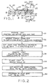
- FIG. 2 is a block diagram chart useful in explaining the fabrication of the invention shown in FIG. 1 (1 inch = 2,54 cm).
- Referring to FIGS. 1 and 2, Nb3Sn
superconducting tape 10 includes a layer of Nb3Sn 12 sandwiched between a pair of layers of stabilizingcopper foil layers -
Superconducting NbTi wire 20 is positioned in contact with one side ofsuperconducting tape 10 andPermeseal retaining tape 28 in the order of 12 mm wide is wrapped around the contact area at approximately 2 inches fromend 21 ofsuperconducting tape 10, and is also wrapped around a region approximately 6 inches from the end as indicated byarrow 24.Permeseal retaining tape 28 is utilized to retainsuperconducting tape 10 andsuperconducting wire 20 in position during subsequent formation of the superconducting joint incontact area 25 betweenend 21 ofsuperconducting tape 10 andPermeseal retaining tape 28 atarrow 24.Permeseal retaining tape 28 atarrow 24 assists in preventing any sharp bending which could damagetape 10. - With
copper stabilizing layers superconducting tape 10 and copper coatedNbTi wire 20 as shown in FIG. 1, the copper is removed incontact area 25 before a superconducting joint is formed between the superconducting tape and wire to enable direct contact between the Nb3Sn and NbTi. This is accomplished by dipping or submerging 52 approximately one and one half inches ofcontact area 25 in a tin bath of 99.9% pure tin heated to 350°C for a period in excess of 15 minutes. Prior to the immersion, the top of the tin bath may be cleaned with a stainless steel spatula to removed any oxides or foreign materials. - Once the
contact area 25 for the joint hascopper layer 14 etched off, the assembly orjoint 8 is removed from the tin bath and immediately transferred 54 to a Pb-Bi bath up to the 1.5 inch mark close toarrow 22. The Pb-Bi bath is at 350°C and joint 8 remains in the bath for a period of approximately 7 to 10 minutes. - Meanwhile, a mold or enclosing
form 30 is set on top or adjacent to the bath to allow it to warm before molding the complete joint. At the end of the 7-10 minute period, theend joint 8 is lifted 56 out of the Pb-Bi bath to -allow the Pb-Bi coated ends ofsuperconducting conductors conductors form 30 consisting of upper half 34 andlower half 32 with a clamp or securingdevice joint 25.Mold 30 had aninternal bore 41 slightly larger in diameter than Pb-Bi coatedconductors end 21, that is approximately up toarrow 22. - The Pb-Bi coated
conductors mold 30 are then submerged 60 into the Pb-Bi bath. Joint 8 includingconductors mold 30 is shaken slightly to remove any air bubbles within the mold and to allow Pb-Bi to be formed withinmold 30 and aroundsuperconductors contact area 25. - Mold 30 and
joint 8 are then carefully lifted out of the bath and transferred 62 to a heat sink stand with the joints being held straight in the mold until the Pb-Bi cools Upon cooling,mold 30 is removed andjoint 8 is complete.Permeseal retaining tape 28 at arrow 26 may be removed, if desired, although this is not necessary. During the process care should be taken not to put sharp bends in the Nb3Sn because of potential damage to the superconducting material. Also care should be taken while clampingsuperconducting conductors mold 30 to prevent overtightening and deformation oftape 12 orjoint 25. - By way of summary, and with particular reference to FIG. 2, the
initial step 50 is to prepare joint 25 by positioning and securingsuperconducting wire 20 andsuperconducting tape 10. Ifsuperconducting tape conductor 10 and/orsuperconducting wire 20 includes a copper stabilizer layer it is necessary to remove 52 the copper from the superconductors in contact area orjoint 25 as indicated byarrow 51. This is accomplished in a tin bath for as much as more than approximately 15 minutes at approximately 350°C with one and one half inches of the end of the contact area being immersed. After the copper layer of encapsulation is removedjoint 8 is removed from the tin bath and immediately transferred to a 350°C PbBi bath 54 for approximately 7-10 minutes after whichjoint 8 is removed 56 from the PbBi bath to allow the Pb-Bi coatedconductors Conductors mold 30 which may be heated by placing it proximate to the heated PbBi bath. Mold 30 andconductors mold 30 is filled with molten PbBi the mold andconductors joint 25 cool.Mold 30 is then removed exposing Pb-Bi coatedsuperconducting joint 25 suitable for use in MRI equipment through the joining of Nb3Snsuperconducting tape 10 and NbTisuperconducting wire 20. - The suitability of
joints 8 fabricated in accordance with the present invention for superconducting use were confirmed by testing which showed adequate and desirable magnetic characteristics.
Claims (10)
- A method of forming superconducting joints for use in superconducting magnets between an Nb3Sn superconductor (10) and NbTi superconductor (20) comprising;positioning said Nb3Sn superconductor into contact with said NbTi superconductor (50) to form a contact area;applying molten Pb-Bi to coat said contact area (54); andallowing said coating to cool (56).
- The method of claim 1 wherein said Pb-Bi is applied in a molten Pb-Bi bath by dipping said contact area into said molten bath.
- The method of claim 2 wherein said bath is maintained at a temperature of approximately 350°C and said dipping is for a period of 7-10 minutes.
- The method of claim 3 wherein a mold (32,34) is positioned around said tape and said wire in the region of said contact area.
- The method of claim 4 wherein said mold is heated and molten Pb-Bi is applied to said contact area within said mold.
- The method of claim 4 wherein the application of Pb-Bi to said contact area within said mold is accomplished by a second dipping (60) of said contact area plus said heated mold into said bath of molten Pb-Bi.
- The method of claim 6 wherein said mold is clamped (58) around said contact area prior to said second dipping.
- The method of claim 7 wherein said Nb3Sn tape superconductor is Nb3Sn sandwiched between copper stabilizing layers (14,16) and said NbTi superconductor is a wire encapsulated in a copper stabilizer and the copper in the region of said contact area is removed prior to said second dipping.
- The method of claim 8 wherein said copper is removed (52) by a different dipping of said contact area into a molten tin bath.
- The method of claim 9 wherein said tin bath temperature is maintained at approximately 350°C and said different dipping is for a period of time in excess of 15 minutes.
Applications Claiming Priority (2)
| Application Number | Priority Date | Filing Date | Title |
|---|---|---|---|
| US08/576,707 US5690991A (en) | 1995-12-21 | 1995-12-21 | Superconducting joint between Nb3 Sn tape and NbTi wire for use in superconducting magnets |
| US576707 | 1995-12-21 |
Publications (3)
| Publication Number | Publication Date |
|---|---|
| EP0806801A2 EP0806801A2 (en) | 1997-11-12 |
| EP0806801A3 EP0806801A3 (en) | 1998-08-12 |
| EP0806801B1 true EP0806801B1 (en) | 2000-04-12 |
Family
ID=24305636
Family Applications (1)
| Application Number | Title | Priority Date | Filing Date |
|---|---|---|---|
| EP96309190A Expired - Lifetime EP0806801B1 (en) | 1995-12-21 | 1996-12-17 | Superconducting joint between Nb3Sn tape and NbTi wire for use in superconducting magnets |
Country Status (4)
| Country | Link |
|---|---|
| US (1) | US5690991A (en) |
| EP (1) | EP0806801B1 (en) |
| JP (1) | JPH1041043A (en) |
| DE (1) | DE69607742T2 (en) |
Families Citing this family (5)
| Publication number | Priority date | Publication date | Assignee | Title |
|---|---|---|---|---|
| US6735848B1 (en) * | 1999-09-24 | 2004-05-18 | Fsu Research Foundation, Inc. | Method of manufacturing a superconducting magnet |
| US7649720B2 (en) * | 2005-05-06 | 2010-01-19 | Florida State University Research Foundation, Inc. | Quench protection of HTS superconducting magnets |
| US8346326B2 (en) * | 2008-01-17 | 2013-01-01 | General Electric Company | Superconductive wire, processes of manufacture and uses thereof |
| US8812069B2 (en) * | 2009-01-29 | 2014-08-19 | Hyper Tech Research, Inc | Low loss joint for superconducting wire |
| KR102154674B1 (en) * | 2018-09-07 | 2020-09-10 | (주)금룡테크 | Method of bonding superconducting wire |
Family Cites Families (5)
| Publication number | Priority date | Publication date | Assignee | Title |
|---|---|---|---|---|
| US3449818A (en) * | 1967-05-16 | 1969-06-17 | North American Rockwell | Superconductor joint |
| DE4017553C1 (en) * | 1990-05-31 | 1991-09-19 | Kernforschungszentrum Karlsruhe Gmbh, 7500 Karlsruhe, De | |
| JPH05121232A (en) * | 1991-10-28 | 1993-05-18 | Toshiba Corp | Current superconductive magnet and its manufacture |
| US5571602A (en) * | 1994-12-29 | 1996-11-05 | General Electric Company | Superconducting joints for superconducting sheets |
| US5597423A (en) * | 1995-12-20 | 1997-01-28 | General Electric Company | Niobium tin sheet for superconducting magnets |
-
1995
- 1995-12-21 US US08/576,707 patent/US5690991A/en not_active Expired - Fee Related
-
1996
- 1996-12-17 DE DE69607742T patent/DE69607742T2/en not_active Expired - Fee Related
- 1996-12-17 EP EP96309190A patent/EP0806801B1/en not_active Expired - Lifetime
- 1996-12-18 JP JP8337377A patent/JPH1041043A/en not_active Withdrawn
Also Published As
| Publication number | Publication date |
|---|---|
| US5690991A (en) | 1997-11-25 |
| EP0806801A2 (en) | 1997-11-12 |
| DE69607742T2 (en) | 2000-11-16 |
| JPH1041043A (en) | 1998-02-13 |
| EP0806801A3 (en) | 1998-08-12 |
| DE69607742D1 (en) | 2000-05-18 |
Similar Documents
| Publication | Publication Date | Title |
|---|---|---|
| EP0423354B2 (en) | Oxide superconductor wire, method of producing the same and article produced therefrom | |
| JP5214744B2 (en) | Superconducting joining method of 2 generation high temperature superconducting wire using heat treatment under reduced oxygen partial pressure | |
| JP2003505848A (en) | Encapsulated ceramic superconductor | |
| US5376755A (en) | Composite lead for conducting an electrical current between 75-80K and 4.5K temperatures | |
| JP6853267B2 (en) | 2nd generation superconducting filaments and cables | |
| EP0951588B1 (en) | Cryogen protected superconducting ceramic tape | |
| JP2923988B2 (en) | Superconducting conductor | |
| US3523361A (en) | Method of splicing superconductive wires | |
| EP0806801B1 (en) | Superconducting joint between Nb3Sn tape and NbTi wire for use in superconducting magnets | |
| KR100964354B1 (en) | Method of joining YBCO-CC superconducting wire by the melting diffusion of two superconductor layers facing each other | |
| CA2011241A1 (en) | Nickel-based substrate for ceramic superconductor | |
| JP3568561B2 (en) | Structure of oxide superconductor with stabilizing metal layer | |
| US6153825A (en) | Superconducting current lead | |
| EP0184184B1 (en) | Mold method for superconductive joint fabrication | |
| KR101343887B1 (en) | Splicing method for superconductive wires containing mg and b | |
| Cheggour et al. | Magnetic-field dependence of the reversible axial-strain effect in Y-Ba-Cu-O coated conductors | |
| EP0445832B1 (en) | Method of producing superconducting ceramic wire having protective metal coating thereon | |
| JP3447990B2 (en) | Superconducting connection method and superconducting connection structure for superconducting wires | |
| KR100964361B1 (en) | Method of joining YBCO-CC superconducting wire by the melting diffusion under the control of partial oxygen pressure | |
| US20220084725A1 (en) | Flexible hts current leads | |
| Solovyov et al. | Performance of layer wound epoxy-impregnated coils made from a multifilamentary cable of exfoliated YBCO | |
| JP2002231523A (en) | Compound-based superconductive coil and its manufacturing method | |
| JP2021182528A (en) | Ultra-low resistance connection method of high-temperature oxide superconductive wire material and metallic superconductive wire material and ultra-low resistance connection body | |
| Martino et al. | Assembly and soldering procedure of nonstabilized YBCO coils for 1000 A SFCL | |
| KR20220046084A (en) | Joint Structure of Multi-filament Core Superconducting Wire And Manufacturing Method Thereof |
Legal Events
| Date | Code | Title | Description |
|---|---|---|---|
| PUAI | Public reference made under article 153(3) epc to a published international application that has entered the european phase |
Free format text: ORIGINAL CODE: 0009012 |
|
| AK | Designated contracting states |
Kind code of ref document: A2 Designated state(s): DE GB NL |
|
| PUAL | Search report despatched |
Free format text: ORIGINAL CODE: 0009013 |
|
| AK | Designated contracting states |
Kind code of ref document: A3 Designated state(s): DE GB NL |
|
| 17P | Request for examination filed |
Effective date: 19990212 |
|
| GRAG | Despatch of communication of intention to grant |
Free format text: ORIGINAL CODE: EPIDOS AGRA |
|
| 17Q | First examination report despatched |
Effective date: 19990806 |
|
| GRAG | Despatch of communication of intention to grant |
Free format text: ORIGINAL CODE: EPIDOS AGRA |
|
| GRAH | Despatch of communication of intention to grant a patent |
Free format text: ORIGINAL CODE: EPIDOS IGRA |
|
| GRAH | Despatch of communication of intention to grant a patent |
Free format text: ORIGINAL CODE: EPIDOS IGRA |
|
| GRAA | (expected) grant |
Free format text: ORIGINAL CODE: 0009210 |
|
| AK | Designated contracting states |
Kind code of ref document: B1 Designated state(s): DE GB NL |
|
| REF | Corresponds to: |
Ref document number: 69607742 Country of ref document: DE Date of ref document: 20000518 |
|
| EN | Fr: translation not filed | ||
| PLBE | No opposition filed within time limit |
Free format text: ORIGINAL CODE: 0009261 |
|
| STAA | Information on the status of an ep patent application or granted ep patent |
Free format text: STATUS: NO OPPOSITION FILED WITHIN TIME LIMIT |
|
| 26N | No opposition filed | ||
| REG | Reference to a national code |
Ref country code: GB Ref legal event code: IF02 |
|
| PGFP | Annual fee paid to national office [announced via postgrant information from national office to epo] |
Ref country code: NL Payment date: 20031203 Year of fee payment: 8 |
|
| PGFP | Annual fee paid to national office [announced via postgrant information from national office to epo] |
Ref country code: GB Payment date: 20031210 Year of fee payment: 8 |
|
| PGFP | Annual fee paid to national office [announced via postgrant information from national office to epo] |
Ref country code: DE Payment date: 20040202 Year of fee payment: 8 |
|
| PG25 | Lapsed in a contracting state [announced via postgrant information from national office to epo] |
Ref country code: GB Free format text: LAPSE BECAUSE OF NON-PAYMENT OF DUE FEES Effective date: 20041217 |
|
| PG25 | Lapsed in a contracting state [announced via postgrant information from national office to epo] |
Ref country code: NL Free format text: LAPSE BECAUSE OF NON-PAYMENT OF DUE FEES Effective date: 20050701 Ref country code: DE Free format text: LAPSE BECAUSE OF NON-PAYMENT OF DUE FEES Effective date: 20050701 |
|
| GBPC | Gb: european patent ceased through non-payment of renewal fee |
Effective date: 20041217 |
|
| NLV4 | Nl: lapsed or anulled due to non-payment of the annual fee |
Effective date: 20050701 |