EP0805577A2 - Procédé de réduction d'impulsions de bruit "ou-câblé" dans une conception de bus à haute performance - Google Patents
Procédé de réduction d'impulsions de bruit "ou-câblé" dans une conception de bus à haute performance Download PDFInfo
- Publication number
- EP0805577A2 EP0805577A2 EP97302463A EP97302463A EP0805577A2 EP 0805577 A2 EP0805577 A2 EP 0805577A2 EP 97302463 A EP97302463 A EP 97302463A EP 97302463 A EP97302463 A EP 97302463A EP 0805577 A2 EP0805577 A2 EP 0805577A2
- Authority
- EP
- European Patent Office
- Prior art keywords
- bus
- going
- driver
- voltage
- signal
- Prior art date
- Legal status (The legal status is an assumption and is not a legal conclusion. Google has not performed a legal analysis and makes no representation as to the accuracy of the status listed.)
- Withdrawn
Links
Images

Classifications
-
- H—ELECTRICITY
- H04—ELECTRIC COMMUNICATION TECHNIQUE
- H04L—TRANSMISSION OF DIGITAL INFORMATION, e.g. TELEGRAPHIC COMMUNICATION
- H04L25/00—Baseband systems
- H04L25/02—Details ; arrangements for supplying electrical power along data transmission lines
- H04L25/0264—Arrangements for coupling to transmission lines
- H04L25/028—Arrangements specific to the transmitter end
-
- H—ELECTRICITY
- H04—ELECTRIC COMMUNICATION TECHNIQUE
- H04L—TRANSMISSION OF DIGITAL INFORMATION, e.g. TELEGRAPHIC COMMUNICATION
- H04L25/00—Baseband systems
- H04L25/02—Details ; arrangements for supplying electrical power along data transmission lines
- H04L25/0264—Arrangements for coupling to transmission lines
- H04L25/0292—Arrangements specific to the receiver end
-
- H—ELECTRICITY
- H04—ELECTRIC COMMUNICATION TECHNIQUE
- H04L—TRANSMISSION OF DIGITAL INFORMATION, e.g. TELEGRAPHIC COMMUNICATION
- H04L25/00—Baseband systems
- H04L25/02—Details ; arrangements for supplying electrical power along data transmission lines
- H04L25/0264—Arrangements for coupling to transmission lines
- H04L25/0278—Arrangements for impedance matching
-
- H—ELECTRICITY
- H04—ELECTRIC COMMUNICATION TECHNIQUE
- H04L—TRANSMISSION OF DIGITAL INFORMATION, e.g. TELEGRAPHIC COMMUNICATION
- H04L25/00—Baseband systems
- H04L25/02—Details ; arrangements for supplying electrical power along data transmission lines
- H04L25/0264—Arrangements for coupling to transmission lines
- H04L25/0298—Arrangement for terminating transmission lines
Definitions
- the invention relates to high performance bus architectures. More specifically, the invention relates to reducing the wire-or glitch in bus design supporting wire-or functions.
- the "wire-or glitch” is a common problem in bi-directional electrical bus design. For example, where open drain drivers are connected to a bus terminated in pull-up resistor, if one driver turns off at the same time as another driver turns on, a wire-or glitch occurs. The problem is exacerbated by line length and line loading.
- the wire-or glitch in the above example is a positive going disturbance which occurs when one driver output turns off (goes high) while the other driver turns on (goes low).
- the glitch is caused by a sudden increase in line current which in turn generates a positive going voltage on the line.
- Some time is required for the on-going driver's output to drive the current back to the original level. Amplitude and length of the glitch depend on three factors: 1) current that the off-going output was conducting; 2) line impedance; and 3) line length between outputs.
- the settling time of the glitch is approximately the round trip delay of the loaded bus.
- cycle time clock to out + propagation delay of bus + setup of input + clock skew.
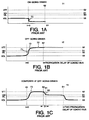
- Figure 1a shows a graph of negative-going wave 11 at the location of the on-going driver of a prior art system.
- Figure 1b shows a graph of a positive-going wave 12 at the location of the off-going driver of a prior art system.
- Figure 1c shows a graph of a composite wave 13 of a prior art wire-or system.
- Composite wave 13 corresponds to sampling the bus 3 at the location of the off-going driver at any instant in time. All three signals are shown relative to the powers supply voltage 52, a high threshold voltage (v ih ) 51, a low threshold voltage (V il ) 50, and a voltage operation level (V ol ) 53.
- V ih high threshold voltage
- V il low threshold voltage
- V ol voltage operation level
- Wave 11 is a negative going voltage created at the on-going driver (going low).
- Wave 12 is the positive going wave created by the off-going driver (going high) as it rapidly rises to V TT 52 before the negative going wave 11 arrives.
- Wave 13 is the composite wave that can be sampled on the bus at the off-going driver. As can be seen, the arrival of the negative going wave 11 only drives the composite wave down to about V ih 51 after the propagation delay. Thus, the bus can not be properly sampled until a negatively reflected wave arrives two propagation delays after the initial switching.
- the propagation delay becomes the most significant part of the overall cycle time.
- the SPARC Center 2,000 work station available from Sun Microsystems of Mountain View, California has ten slot backplane bus which supports wire-or functions at 40 MHz.
- the loaded bus one-way propagation delay is approximately 5 ns. Therefore, the bus settling time is the round trip of the loaded bus delay, approximately 10 ns. Accordingly, 10 ns of the 25 ns of cycle time are absorbed by the wire-or glitch settling time.
- a system and method of reducing wire-or glitch to improve bus speeds is disclosed.
- the rise time of the wave created by the off-going driver (going high) is controlled.
- the off-going wave is forced to climb gradually such that one propagation delay of the loaded bus later, it is only marginally above a high threshold voltage.
- the fall time of the wave created by an on-going driver (going low) is minimized such that a strong negative going voltage propagates down the bus. This strong negative going voltage drags a composite wave on the bus (i.e. the combination of the waves of the on-going driver and the off-going driver) back below a low threshold voltage approximately one propagation delay after the switching occurs.
- Figures 1a, 1b , and 1c are graphs of wave forms on the bus in a prior art system.
- Figure 2 is a diagram of a bus supporting wire-or and employing one embodiment of the invention.
- Figures 3a, 3b , and 3c are graphs of wave forms on the bus in one embodiment of the invention.
- FIG. 2 shows a diagram of a bus system supporting wire-or functions and employing the instant invention.
- Bus 3 is coupled to a power supply 1 supplying a voltage of V tt through termination resistors (R t ) 2 at either end of the bus.
- a plurality of drivers here on-going driver 6 and off-going driver 7, are coupled to the bus.
- Each driver is coupled to the bus through a series resistor (R s ).
- R s 5 and R s 4 corresponding to the on-going driver 6 and off-going driver 7, respectively, have the same nominal resistance. If on-going driver 6 turns on the same time off-going driver 7 turns off, on-going driver 6 generates a negative going voltage wave 9 which propagates down the bus away from on-going driver 6.
- off-going driver 7 generates a positive going voltage wave 8 which propagates down the bus away from off-going driver 7.
- the rise time of positive going wave 8 and the fall time of negative going wave 9 as discussed further below, it is possible to reduce the wire-or glitch such that only a single propagation delay is required before the bus 3 can be correctly sampled.
- the series resistors are omitted entirely.
- Reflection contributes to the wire-or glitch.
- the reflection coefficient ((R dr +R s )//R t )-Z load ((R dr +R s )//R t )+Z load
- R dr is the on/off resistance of the driver
- Z load is the loaded impedance of the transmission line given by the equation
- Z load Line impedance/(sqrt (1+ C load C line )).
- Line impedance is the unloaded impedance of the bus 3.
- Cline is the trace capacitance per section between each slot.
- C load is the capacitance of a daughter card including connector pin, board trace, chip circuit, and package loading.
- Zload should be kept as low as possible.
- a trace line with line impedance of 27 ⁇ ⁇ 10% is employed, C line is approximately 5.5 pf, and typical C load is approximately 12.5 pf.
- R dr is approximately 7.5 ⁇ , and R s is nominally 8 ⁇ . Accordingly, Z load is approximately 14.9 ⁇ , which gives a reflection coefficient of-17.5%.
- a sixteen inch backplane fully loaded with sixteen slots can be operated at 83.5 MHz provided that the rise time and fall time of the off-going driver 6 and ongoing driver 7, respectively, are appropriately controlled. Control of rise time and fall time is discussed more fully below.
- An additional advantage is achieved by reducing the intrinsic impedance of the bus 3. Specifically, propagation delay due to loading is reduced.
- the 27 ⁇ transmission line of one exemplary embodiment has a C line of 5.5 pf as compared to the 3 pf C line of typical 50 ⁇ transmission lines.
- the loaded delay is 80% greater than the unloaded delay, while in the typical system, the loaded delay would be 130% greater than the unloaded delay.
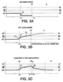
- Figures 3a, b, and c show graphs of negative-going wave 9 at the location of the on-going driver, positive-going wave 8 at the location of the off-going driver, and a composite wave 10 for one exemplary embodiment of the instant invention respectively.
- Composite wave 10 corresponds to sampling the bus 3 at the location of the off-going driver at any instant in time. All three signals are shown relative to the powers supply voltage 52, a high threshold voltage (V ih ) 51, a low threshold voltage (V il ) 50, and a voltage operation level (V ol ) 53.
- V ih high threshold voltage
- V il low threshold voltage
- V ol voltage operation level
- Propagation time 62 is one propagation delay of the loaded bus beyond switching time 64.
- the voltage of the off-going driver jumps to a predetermined voltage 73 below V il 50, and then begins a gradual ascent 72 towards V tt 52. Because the voltage jump 71 remains within the range that can be sampled low, this jump 71 does not prevent control of the wire-or glitch. Rather, the jump 71 reduces the voltage range over which the gradual ascent 72 is controlled. In the instant invention, the gradual ascent 72 is controlled to ensure that one propagation delay 62 later, the off-going driver signal 8 will be only marginally above V ih 51. The relatively narrow voltage range over which the rise must be controlled increases both the accuracy and ease of such control.
- the ongoing driver drives a voltage of predetermined drop below V ol 53:
- the fall time 70 is minimized.
- the fall time 70 is shown as an ideal instantaneous drop.
- Rs exacerbates the slewing. Therefore, it is important to control the slewing so that the slewing is minimized and the fall time occurs as rapidly as possible.
- This fast fall time 70 creates a strong negative-going wave 9 which propagates down the bus 3 and one propagation delay later, creates a composite wave 10 at the location of off-going driver 7.
- the composite wave 10 is pulled down proportionally to the difference in slope of the positive going wave 8 and the negative going wave 9.
- the composite wave will be pulled back below V il 50 ⁇ t 61 after one propagation delay of the loaded bus (e.g., fall time equals ⁇ t).
- fall time 70 goes to 0
- ⁇ t also goes to 0
- the bus will be able to be accurately sampled one propagation delay after switching time 64.
- the rise time of the off-going driver can be controlled in several ways. Among the possible ways are delayed turn-on of transistors. Under this method, instead of a single large transistor, multiple smaller transistors are used to form the driver. By turning the small transistors on individually over time, the voltage appearing on the bus and, thus, the effective rise time increases in gradual steps. Alternatively, by controlling the voltage at the gate of the driver and gradually increasing it, the transition from completely off to on or vice versa can be controlled. However, because the transition range between on and off is typically quite narrow, it is difficult to effectively control the voltage over a significant range. Another alternative is to control the slew rate of the off-going driver to maximize the slewing. It is also possible to combine any or all of the above methods of controlling the rise time.
- jump 71 is eliminated and gradual ascent 72 begins from V ol 53.
- the positive going voltage wave 8 should still be only marginally above V ih 51 when the negative going voltage wave 9 arrives one propagation delay later 62.
Landscapes
- Engineering & Computer Science (AREA)
- Power Engineering (AREA)
- Computer Networks & Wireless Communication (AREA)
- Signal Processing (AREA)
- Logic Circuits (AREA)
- Electronic Switches (AREA)
- Dc Digital Transmission (AREA)
Applications Claiming Priority (2)
| Application Number | Priority Date | Filing Date | Title |
|---|---|---|---|
| US08/640,096 US6310489B1 (en) | 1996-04-30 | 1996-04-30 | Method to reduce wire-or glitch in high performance bus design to improve bus performance |
| US640096 | 1996-04-30 |
Publications (2)
| Publication Number | Publication Date |
|---|---|
| EP0805577A2 true EP0805577A2 (fr) | 1997-11-05 |
| EP0805577A3 EP0805577A3 (fr) | 2002-06-26 |
Family
ID=24566825
Family Applications (1)
| Application Number | Title | Priority Date | Filing Date |
|---|---|---|---|
| EP97302463A Withdrawn EP0805577A3 (fr) | 1996-04-30 | 1997-04-10 | Procédé de réduction d'impulsions de bruit "ou-câblé" dans une conception de bus à haute performance |
Country Status (3)
| Country | Link |
|---|---|
| US (1) | US6310489B1 (fr) |
| EP (1) | EP0805577A3 (fr) |
| JP (1) | JPH1083234A (fr) |
Cited By (1)
| Publication number | Priority date | Publication date | Assignee | Title |
|---|---|---|---|---|
| US6219812B1 (en) * | 1998-06-11 | 2001-04-17 | Sun Microsystems, Inc. | Apparatus and method for interfacing boundary-scan circuitry with DTL output drivers |
Families Citing this family (2)
| Publication number | Priority date | Publication date | Assignee | Title |
|---|---|---|---|---|
| US6985004B2 (en) | 2001-02-12 | 2006-01-10 | International Business Machines Corporation | Wiring optimizations for power |
| US9094068B2 (en) * | 2013-10-11 | 2015-07-28 | Entropic Communications, Llc | Transmit noise and impedance change mitigation in wired communication system |
Family Cites Families (6)
| Publication number | Priority date | Publication date | Assignee | Title |
|---|---|---|---|---|
| US3694665A (en) * | 1970-11-05 | 1972-09-26 | Sanders Associates Inc | Wired or circuit |
| US4849659A (en) * | 1987-12-15 | 1989-07-18 | North American Philips Corporation, Signetics Division | Emitter-coupled logic circuit with three-state capability |
| US5179299A (en) * | 1990-11-05 | 1993-01-12 | Ncr Corporation | Cmos low output voltage bus driver |
| US5136187A (en) * | 1991-04-26 | 1992-08-04 | International Business Machines Corporation | Temperature compensated communications bus terminator |
| US5239559A (en) * | 1991-11-08 | 1993-08-24 | Methode Electronics, Inc. | Terminator method and apparatus |
| JP2882266B2 (ja) * | 1993-12-28 | 1999-04-12 | 株式会社日立製作所 | 信号伝送装置及び回路ブロック |
-
1996
- 1996-04-30 US US08/640,096 patent/US6310489B1/en not_active Expired - Lifetime
-
1997
- 1997-04-10 EP EP97302463A patent/EP0805577A3/fr not_active Withdrawn
- 1997-04-28 JP JP9122901A patent/JPH1083234A/ja active Pending
Cited By (1)
| Publication number | Priority date | Publication date | Assignee | Title |
|---|---|---|---|---|
| US6219812B1 (en) * | 1998-06-11 | 2001-04-17 | Sun Microsystems, Inc. | Apparatus and method for interfacing boundary-scan circuitry with DTL output drivers |
Also Published As
| Publication number | Publication date |
|---|---|
| JPH1083234A (ja) | 1998-03-31 |
| EP0805577A3 (fr) | 2002-06-26 |
| US6310489B1 (en) | 2001-10-30 |
Similar Documents
| Publication | Publication Date | Title |
|---|---|---|
| US7123048B2 (en) | Signal transmitting device suited to fast signal transmission | |
| US6344765B2 (en) | Signal transmission with reduced ringing of signals | |
| US5760601A (en) | Transmission line driver circuit for matching transmission line characteristic impedance | |
| US6704818B1 (en) | Voltage-mode driver with pre-emphasis, slew-rate control and source termination | |
| US5898326A (en) | Signal transmission cable driver apparatus without a peaking coil | |
| US20050280435A1 (en) | Output buffer with time varying source impedance for driving capacitively-terminated transmission lines | |
| US4675551A (en) | Digital logic bus termination using the input clamping Schottky diodes of a logic circuit | |
| US6420899B1 (en) | Dynamic impedance matched driver for improved slew rate and glitch termination | |
| EP0542321A2 (fr) | Procédé et circuit pour contrôler les réflexions de tension sur des lignes de transmission | |
| US20250330160A1 (en) | Serial bus redriver with trailing edge boost circuit | |
| US20030161196A1 (en) | High-speed memory system | |
| US6310489B1 (en) | Method to reduce wire-or glitch in high performance bus design to improve bus performance | |
| US5650757A (en) | Impedance stepping for increasing the operating speed of computer backplane busses | |
| US6434647B1 (en) | Reflected-wave bus termination | |
| US5485107A (en) | Backplane driver circuit | |
| US20020051506A1 (en) | Transmitter circuit comprising timing deskewing means | |
| US7142006B2 (en) | Device and method to cause a false data value to be correctly seen as the proper data value | |
| US5514979A (en) | Methods and apparatus for dynamically reducing ringing of driver output signal | |
| US5917335A (en) | Output voltage controlled impedance output buffer | |
| US5852372A (en) | Apparatus and method for signal handling on GTL-type buses | |
| JPH05335928A (ja) | 集積回路用信号線パルス向上回路 | |
| EP0865042A3 (fr) | Circuit d'attaque et dispositif de mémoire à semiconducteurs l'utilisant | |
| US6512396B1 (en) | High speed data processing system and method | |
| US7256617B2 (en) | Method and apparatus to linearize output buffer and on-chip termination | |
| US5093587A (en) | ECL bidirectional bus for use in a network with modules which employs high resistance interconnect technology between module |
Legal Events
| Date | Code | Title | Description |
|---|---|---|---|
| PUAI | Public reference made under article 153(3) epc to a published international application that has entered the european phase |
Free format text: ORIGINAL CODE: 0009012 |
|
| AK | Designated contracting states |
Kind code of ref document: A2 Designated state(s): DE FR GB IT NL SE |
|
| PUAL | Search report despatched |
Free format text: ORIGINAL CODE: 0009013 |
|
| AK | Designated contracting states |
Kind code of ref document: A3 Designated state(s): DE FR GB IT NL SE |
|
| 17P | Request for examination filed |
Effective date: 20021204 |
|
| RAP1 | Party data changed (applicant data changed or rights of an application transferred) |
Owner name: SUN MICROSYSTEMS, INC. |
|
| STAA | Information on the status of an ep patent application or granted ep patent |
Free format text: STATUS: THE APPLICATION IS DEEMED TO BE WITHDRAWN |
|
| 18D | Application deemed to be withdrawn |
Effective date: 20031101 |