EP0804000A2 - RDS signal detection device - Google Patents
RDS signal detection device Download PDFInfo
- Publication number
- EP0804000A2 EP0804000A2 EP97302747A EP97302747A EP0804000A2 EP 0804000 A2 EP0804000 A2 EP 0804000A2 EP 97302747 A EP97302747 A EP 97302747A EP 97302747 A EP97302747 A EP 97302747A EP 0804000 A2 EP0804000 A2 EP 0804000A2
- Authority
- EP
- European Patent Office
- Prior art keywords
- signals
- rds
- circuit
- biphase
- output
- Prior art date
- Legal status (The legal status is an assumption and is not a legal conclusion. Google has not performed a legal analysis and makes no representation as to the accuracy of the status listed.)
- Granted
Links
Images


Classifications
-
- H—ELECTRICITY
- H04—ELECTRIC COMMUNICATION TECHNIQUE
- H04L—TRANSMISSION OF DIGITAL INFORMATION, e.g. TELEGRAPHIC COMMUNICATION
- H04L27/00—Modulated-carrier systems
- H04L27/18—Phase-modulated carrier systems, i.e. using phase-shift keying
- H04L27/22—Demodulator circuits; Receiver circuits
- H04L27/233—Demodulator circuits; Receiver circuits using non-coherent demodulation
- H04L27/2332—Demodulator circuits; Receiver circuits using non-coherent demodulation using a non-coherent carrier
-
- H—ELECTRICITY
- H04—ELECTRIC COMMUNICATION TECHNIQUE
- H04H—BROADCAST COMMUNICATION
- H04H60/00—Arrangements for broadcast applications with a direct linking to broadcast information or broadcast space-time; Broadcast-related systems
- H04H60/35—Arrangements for identifying or recognising characteristics with a direct linkage to broadcast information or to broadcast space-time, e.g. for identifying broadcast stations or for identifying users
- H04H60/38—Arrangements for identifying or recognising characteristics with a direct linkage to broadcast information or to broadcast space-time, e.g. for identifying broadcast stations or for identifying users for identifying broadcast time or space
- H04H60/41—Arrangements for identifying or recognising characteristics with a direct linkage to broadcast information or to broadcast space-time, e.g. for identifying broadcast stations or for identifying users for identifying broadcast time or space for identifying broadcast space, i.e. broadcast channels, broadcast stations or broadcast areas
- H04H60/44—Arrangements for identifying or recognising characteristics with a direct linkage to broadcast information or to broadcast space-time, e.g. for identifying broadcast stations or for identifying users for identifying broadcast time or space for identifying broadcast space, i.e. broadcast channels, broadcast stations or broadcast areas for identifying broadcast stations
-
- H—ELECTRICITY
- H04—ELECTRIC COMMUNICATION TECHNIQUE
- H04H—BROADCAST COMMUNICATION
- H04H20/00—Arrangements for broadcast or for distribution combined with broadcast
- H04H20/20—Arrangements for broadcast or distribution of identical information via plural systems
- H04H20/22—Arrangements for broadcast of identical information via plural broadcast systems
-
- H—ELECTRICITY
- H04—ELECTRIC COMMUNICATION TECHNIQUE
- H04H—BROADCAST COMMUNICATION
- H04H2201/00—Aspects of broadcast communication
- H04H2201/10—Aspects of broadcast communication characterised by the type of broadcast system
- H04H2201/13—Aspects of broadcast communication characterised by the type of broadcast system radio data system/radio broadcast data system [RDS/RBDS]
-
- H—ELECTRICITY
- H04—ELECTRIC COMMUNICATION TECHNIQUE
- H04L—TRANSMISSION OF DIGITAL INFORMATION, e.g. TELEGRAPHIC COMMUNICATION
- H04L27/00—Modulated-carrier systems
- H04L27/0014—Carrier regulation
- H04L2027/0024—Carrier regulation at the receiver end
- H04L2027/0026—Correction of carrier offset
- H04L2027/0028—Correction of carrier offset at passband only
-
- H—ELECTRICITY
- H04—ELECTRIC COMMUNICATION TECHNIQUE
- H04L—TRANSMISSION OF DIGITAL INFORMATION, e.g. TELEGRAPHIC COMMUNICATION
- H04L27/00—Modulated-carrier systems
- H04L27/0014—Carrier regulation
- H04L2027/0044—Control loops for carrier regulation
- H04L2027/0046—Open loops
- H04L2027/0048—Frequency multiplication
Definitions
- Fig. 5 is a circuit diagram showing a configuration of a pair judgment circuit.
- the data clock regenerator circuit 10 judges pairs of biphase symbol data based on the output from the D-FF8. At timings of every other symbol to be paired, the data clock regenerator circuit 10 then separates clock signals from biphase clock signals which were regenerated at each symbol. The data clock regenerator circuit 10 then supplies these clock signals to both D-FFs 94, 16 and also to a differential decoder circuit 11 as data clock signals shown in (g). Therefore, differentially coded RDS data outputted from the subtraction circuit 91 and the judgment data from the data judgment circuitry 15 are latched into D-FFs 94 and 16 at every two biphase symbols constituting a pair.
Landscapes
- Engineering & Computer Science (AREA)
- Signal Processing (AREA)
- Computer Networks & Wireless Communication (AREA)
- Circuits Of Receivers In General (AREA)
- Dc Digital Transmission (AREA)
Abstract
Description
- The present invention relates to an Radio Data System (RDS) signal detection device incorporated in a device to receive and demodulate RDS broadcasting signals, which judges whether signals received are RDS signals or not.
- In an RDS broadcast mainly broadcast in Europe, automatic reception control of broadcasting stations which broadcast the same programs is performed using Alternative Frequency (AF) codes contained in data transmitted. In this case, it is necessary to search for a station having the best reception among stations listed in an AF code list and broadcasting the same program. It is also necessary to switch to the selected station as soon as possible. Therefore, selection of the best reception station has been conventionally performed by detecting the strength of reception electric field at each station while output sounds are muted for a very brief duration that is not uncomfortable for listeners so that a reception station is switched to an AF station.
- In reception control as described above, the reception station selected according to the AF code can be a non-RDS station, or reception sensitivity of the station is sometimes not good enough to receive RDS data. In cases like these, a Program Identification code (PI code) for judging whether the station selected is a station to broadcast the same program is not detected, and as a consequence selection of a proper station is not performed. Therefore, re-selection of a station on the AF list having a second best strength of reception electric field is performed. For a quicker, more accurate selection, it is necessary to judge, as soon as possible, whether a station switched to is an RDS station or not. Likewise, if only RDS stations are sought and selected or memorized, it is necessary to judge, as soon as possible, whether the station selected is an RDS station or not.
- A judging action of an RDS station such as that described above has conventionally been performed by detecting block synchronization or group synchronization of RDS data after broadcasting signal reception has been started by the selected station which was assumed to be an AF station.
- The RDS data is configured in blocks of 26 bits. A certain synchronization pattern (offset words) is added to each block. Block synchronization is established by detecting the periodicity of the patterns. One group is configured in four blocks, and group synchronization is established by judging an order of offset words.
- Conventionally, at least 44 msec, which is equivalent to the length of two blocks, was necessary, since synchronization establishment of RDS data was used to judge an RDS station. Depending on reception conditions, about 200 msec is necessary for judgment because more than 100 msec is necessary for synchronization establishment. Therefore, switching of reception stations may be delayed, or listeners may feel uncomfortable due to a long muting period.
- RDS signals are differentially coded and then biphase coded to suppress power of signals with closer carrier frequencies. In biphase coding, for example, a signal of
data 1 is expressed by (1,0), and (0,1) is for a signal of 0. Therefore, one symbol is converted and coded into two symbols. The amplitudes of the carrier frequency signals are modulated by the biphase coding signals. They are then multiplexed into FM base band signals and become actual broadcasting waves. - The present invention takes advantage of the RDS signals which are biphased, and judges whether received signals are RDS signals or not by detecting the existence of pairs of coded symbols within the received signals.
- In other words, the present invention distinguishes RDS signals by first detecting inversion of signals within a biphase symbol pair and then by detecting continuity or a ratio of inversion for a certain duration. Another method of RDS signal judgment is to detect, using the same method as described above, stability of output from a pair judgment circuit which detects a combination of biphase symbols.
- As described above, it is possible to distinguish an RDS station, before synchronization detection of RDS data, for a much shorter time (e.g., 20 msec) by detecting RDS signals using a demodulator using a characteristic of biphase signals.
- Fig. 1 is a block diagram showing an embodiment of a configuration of a data decision circuit of the present invention.
- Fig. 2 is a block diagram showing another configuration of a data decision circuit.
- Fig. 3 is a circuit diagram showing a configuration of a low-pass filter.
- Fig. 4 is a block diagram showing a configuration of a data clock regenerator circuit .
- Fig. 5 is a circuit diagram showing a configuration of a pair judgment circuit.
- Fig. 6 is a timing chart explaining actions described in the embodiment of the present invention.
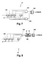
- Fig. 7 is a circuit diagram showing a configuration of an RDS-ID detector circuit.
- Fig. 8 is a circuit diagram showing another configuration of an RDS-ID detector circuit.
- Fig. 9 is a block diagram showing another embodiment of the present invention.
- Fig. 1 is a block diagram of an RDS demodulator related to the present invention.
- FM composite signals in which RDS signals are multiplexed are supplied to a 57KHz-
BPF circuit 1. RDS signals are then separated by the 57 KHz-BPF circuit 1, and supplied to acomparator 2 where the RDS signals are digitized into 0 or 1. Output from the comparator is supplied to both acarrier regenerator circuit 3 and a D flip-flop (hereafter called D-FF) 4 which is a phase detector circuit. On the other hand, clock signals synchronizing a carrier of 57 KHz are regenerated at thecarrier regenerator circuit 3. Based on the regenerated clock signals, D-FF 4 samples the output from thecomparator 2. - Fig. 6 shows waveforms of signals. As a BPF output, RDS signals of Fig. 6(a) are output. Digital signals (b) are output from the
comparator 2. Clock signals of 57 KHz regenerated by thecarrier regenerator circuit 3 are supplied to the D-FF4 on timings shown in (c) (with 90 ° of phase shift from carrier signals) . As a consequence, signals shown in (d) are obtained as the sampling output from the D-FF 4. These signals (d) are supplied to both a biphaseclock regenerator circuit 5 and adata decision circuit 13. In the biphaseclock regenerator circuit 5, clock pulses at a biphase symbol rate shown in (e) are regenerated. In thedata decision circuit 13, anadder 6 adds output from a D-FF 7 which the output of theadder 6 is supplied with, and output from the D-FF 4 shown in (d). The D-FF 7 is reset by the clock pulses at the biphase symbol rate shown in (e). The D-FF 7 and theadder 6 form an accumulator. The sampling output data from the D-FF 4 are accumulated by the accumulator for one symbol period. More specifically, the number of "1"s in the sampling output data is accumulated. - If the sampling data are ideal, signals of 24 carriers during one symbol period are input in the case of RDS signals. Therefore, the accumulation by the adder should result in 24 or 0 (6 or 0 in Fig. 6) . A D-
FF 8 latches the accumulation result using the clock pulses shown in (e) at the biphase symbol rate. The latched result is input into both abiphase decoder circuit 9 and a dataclock regenerator circuit 10. - The
biphase decoder circuit 9 includes both a D-FF 90 which delays the output from the D-FF8 by one biphase period using the clock pulses (e) at the biphase symbol rate, and asubtraction circuit 91 which subtracts the output of the D-FF8 from the output of the D-FF 90. A differential process is performed between neighboring biphase symbol data by both the D-FF 90 and thesubtraction circuit 91. The differentially coded bit is supplied to a D-FF 94 as differentially coded RDS data. The biphase symbol data are expressed as (1,0) for source data of 1, and as (0,1) for source data of 0. Therefore, if the differential result is positive, then the differentially coded RDS data is 1. If the differential result is negative, then the differentially coded RDS data is 0. - The differential result from the
subtraction circuit 91 is also supplied to adata judgment circuitry 15 where an absolute value of the differential result is compared with control data P of an external source. If ideal, noise-free RDS signals are input, the differential result from thesubtraction circuit 91 between the neighboring biphase symbol data should be 24-0=24 or 0-24=-24. The differential result should be large in this case even if there is only a minor effect due to noise or the like. On the other hand, if the input signals are not RDS signals, the differential result should be smaller due to the fact that the signals were not biphase coded. Therefore, in thedata judgment circuitry 15, if the differential result falls within a range from -5 to +5, assuming that the control data P is ±5 for example, the input signals are judged not to be biphase coded signals, in other words, not to be RDS signals. Thedata judgment circuitry 15 then outputs 0 as judgment data. If the differential result does not fall within the previous range, then thedata judgment circuitry 15 judges the input signals to be biphase coded RDS signals, andoutputs 1 as the judgment data. - The data
clock regenerator circuit 10 judges pairs of biphase symbol data based on the output from the D-FF8. At timings of every other symbol to be paired, the dataclock regenerator circuit 10 then separates clock signals from biphase clock signals which were regenerated at each symbol. The dataclock regenerator circuit 10 then supplies these clock signals to both D-FFs differential decoder circuit 11 as data clock signals shown in (g). Therefore, differentially coded RDS data outputted from thesubtraction circuit 91 and the judgment data from thedata judgment circuitry 15 are latched into D-FFs - The differentially coded RDS data latched into the D-
FF 94 are supplied to adifferential decoder circuit 11. Consecutive differentially coded RDS data are decoded into RDS source data by a D-FF 110 and anEXOR circuit 112, and then supplied to a later-described synchronization regenerator circuit where synchronization is established based on the RDS source data. The judgment data latched into the D-FF 16 are supplied to an RDS-ID detector circuit 14 where the signals input are examined to see whether they are RDS signals or not using the judgment data. - In the embodiment described above, the accumulator (the
adder 6 and the D-FF 7) which simply accumulates sampling data for one symbol period is used in thedata decision circuit 13 to obtain an accumulation result of the sampling output. A low-pass filter can be substituted for the accumulator, however. - As shown in Fig. 2, a digital low-
pass filter 12 of 2375 KHz pass band which is the RDS biphase symbol rate is provided instead of theadder 6 and the D-FF 7. Sampling output from the D-FF 4 is supplied to the low-pass filter 12. The biphaseclock regenerator circuit 5 is constructed so that clock signals at the biphase symbol rate as shown in (k) are generated at about a midpoint of each symbol period. The biphase clock signals (k) are supplied to a clock terminal of the D-FF 8, and the D-FF 8 latches output from the digital low-pass filter 12. If decimal places obtained by filtering calculation are output as latch output from the D-FF 8, a plurality of bits including decimal places are obtained as the output. In other words, the latch output should be 1.00 or 0.00 if the input signals are ideal ones free of noise. If waveforms of the input signals are distorted due to noise or the like, then latch output of about 0.50 should be obtained. The latch output is supplied to both thebiphase detector circuit 9 and the dataclock regenerator circuit 10, as previously described. Thebiphase decoder circuit 9 performs differential calculation between biphase symbol data forming a pair. If the differential result is positive, then differentially coded RDS data become 1. If the differential result is negative, then differentially coded RDS data become 0. If ideal noise-free RDS data are input into thebiphase decoder circuit 9, then the differential result should become 1.00-0.00=+1 or 0.00-1.00=-1.00. Even if effects caused by noise are present, the differential result should be large. On the other hand, if the input signals are not RDS signals, then the differential result should take a smaller value due to the fact that the input signals were not biphase coded. Therefore, a threshold value of thedata judgment circuitry 15 is set to be ±0.3. If the differential result falls within a range from -0.3 to +0.3, then the input signals are not RDS signals, andjudgment data 0 is supplied. If the differential result does not fall within the previous range, then the input signals are judged to be RDS signals, andjudgment data 1 is supplied. - The differentially coded RDS data and the judgment data obtained as described above are respectively supplied to the
differential decoder circuit 11 and the RDS-ID detection circuit 14 where RDS source data and RDS-ID signals are respectively outputted. - As the digital low-
pass filter 12, a circuit shown in Fig. 3 which comprises a plurality of delay circuits and a slice circuit can be used. The latch timing of the filter output is set to be about a midpoint of each symbol period, because the filter output is maximized around these timings. Specifically, it is preferable to delay each latch timing by a delay caused by the filter. - A configuration of the data
clock regenerator circuit 10 will now be explained. - In the data
clock regenerator circuit 10, the output from the D-FF 8 is supplied to apair judgment circuit 100 as shown in Fig. 4. Thepair judgment circuit 100 judges timings to be paired using, for example, three consecutive biphase symbol data, and supplies a judgment result to anEXOR 102. Signals obtained by dividing the biphase clock pulses (e) into two using adivider 101 are also supplied to theEXOR circuit 102. After theEXOR circuit 102 supplies output to an ANDcircuit 103, the ANDcircuit 103 separates timings to be paired at every other symbol from the biphase clock signals (e) which were regenerated at every symbol. The separated clocks are supplied as data clocks shown in (g). - More specifically, in the timing chart depicted in Fig. 6, biphase clock signals (e) were divided into two and output as signals shown in (i). When the
pair judgment circuit 100 outputs signals depicted in (h), i.e., 1, theEXOR circuit 102 outputs signals depicted in (j) which are inversions of (i). The ANDcircuit 103 outputs the clock signals (g) at timings of every other symbol. Thepair judgment circuit 100 judges pairs of biphase symbol data based on the output (f) from the D-FF 8. Thepair judgment circuit 100 outputs the signals depicted in (h) which are atlevel 1 in the case of biphase symbol data being paired as (D1, D2), (D3, D4)... The pair judgment circuit outputs the signals depicted in (h) which are atlevel 0 in the case of biphase symbol data being paired as (D0, D1), (D2, D3)... In Fig. 6, the case of biphase symbol data being paired as (D1,D2)... is shown. - The
pair judgment circuit 100 is constructed as shown in Fig. 5. The most significant bit (MSB) of the sequentially input biphase symbol data is supplied to ashift register 201. MSBs a0, al, a2 of the three consecutive biphase symbol data D0, D1, D2 are compared every two bits. Among the bits a0, a1, and a2 in theshift register 201, if a0 and al are exactly the same, anEXNOR circuit 202outputs 1. If a1 and a2 are not the same, anEXOR circuit 203outputs 1. Based on these ls, an ANDcircuit 204outputs 1 and an RS flip-flop circuit 206 is set and outputs 1. D1 and D2 are then judged to be a pair. If a0 is different from al, the output from theEXNOR circuit 202 is 0. If a1 is the same as a2, the output from theEXOR circuit 203 is 0. Based on these 0s, an NORcircuit 205outputs 1. The RS flip-flop 206 is reset and outputs 0. D0 and D1 are then judged to be a pair. As the pair judgment circuit, another circuit such as described in Japanese Patent Application No. Hei6-172682 filed by the applicant of the present invention can be used. - A configuration of the RDS-
ID detector circuit 14 will now be explained in detail. - The RDS-
ID detector circuit 14 is constructed as shown in Fig. 7. Judgment data from the D-FF 16 is supplied to shiftregisters 140 of n-steps. Shift procedure is performed on the shift registers 140 for every data, using the data clock signals (g) output from the dataclock regenerator circuit 10. Output from each register is supplied to both an ANDcircuit 141 and a NORcircuit 142. Output from the ANDcircuit 141 is supplied to a set terminal of an RS-FF143, while output from the NOR circuit is supplied to a reset terminal of the RS-FF143. As a result, RDS-ID signals are obtained. Only if differential results exceed a control data level in all bits of n-bit data, i.e., a case of a biphase pair, are the RDS-ID signals supplied to show that the received signals are RDS signals. On the other hand, if the differential results do not exceed the control data level in all n bits, i.e., a case of biphase data which do not form a pair, the RDS-ID output should be reset. By this procedure, detection conditions for RDS-ID signals become tighter. Once the RDS-ID signals are detected, they are cancelled only when the received signals are absolutely judged not to be RDS signals. - Another example of an RDS-ID detector circuit is shown in Fig. 8. Output from the n-step shift registers 140 is added by an
adder 144, and the addition result is supplied to acomparator 145. In thecomparator 145, based on predetermined values A, B (A>B) supplied from an external source , a set signal is supplied to the RS-FF 143 if the addition result exceeds A. If the addition result is smaller than B, a reset signal is supplied to the RD-FF 143. In this way, the RDS-ID signal is supplied when more than the predetermined number of bits among the n bits satisfy the biphase pair conditions. If less than the predetermined number of bits among the n bits satisfy the biphase pair conditions, output of the RDS-ID signal is reset. In other words, detection of RDS-ID signals has a hysterisis characteristic. - In the above two examples, detection of RDS signals is performed based on the judgment data from the
data judgment circuitry 15. However, it is also possible to judge RDS signals based on the stability of output from thepair judgment circuit 100 in the dataclock regenerator circuit 10. - As shown in Fig. 9, output (h) from the
pair judgment circuit 100 in the dataclock regenerator circuit 10 is supplied, instead of output from the D-FF 16 in Fig. 1, to the RDS-ID detector circuit 14 which has the same configuration as shown in Fig. 8. - Output (h) from the
pair judgment circuit 100 in the dataclock regenerator circuit 10 is supplied to shiftregisters 146 of n-steps which perform shift procedure, and output from each register is added by anadder 147. Output from theadder 147 is compared by acomparator 148 with predetermined values C,D (C<D) set by an external source. If the addition result is equal to or smaller than C or equal to or greater than (n-C), a set signal is supplied to an RS-FF149. If the addition result is equal to or greater than D and equal to or smaller than (n-D), a reset signal is supplied to the RS-FF 149. - The
pair judgment circuit 100, as described above, judges pairs of biphase symbol data which are sequentially input. The circuit is configured so that output is atlevel 1 in the case of biphase symbol data being paired as (D1, D2), (D3, D4)..., and atlevel 0 in the case of biphase symbol data being paired as (D0, D1), (D2, D3) ... Therefore, thepair judgment circuit 100 always outputs 1 or 0 as long as RDS signals are supplied. As a consequence, output of n-bit addition from theadder 147 should be 0 or closer to n if RDS signals were supplied. If input signals were not RDS signals, n-bit addition result tends to be a medium value between 0 and n. - Therefore, when the addition result is compared by the
comparator 148 with the predetermined values as described above, RDS-ID signals are output if the predetermined number of bits among n bits satisfy biphase pair conditions. If the number of bits which satisfy the biphase pair conditions is smaller than the predetermined number of bits, RDS-ID signal output is reset. Judgment of RDS signals can be performed as described above. - It is possible to tighten or loosen RDS-ID detection conditions by changing the control data P, the predetermined values A,B,C,D, and the bit length n of the shift registers 140 and 146. The detection conditions are tightened if the control data P, the predetermined values A, B, and the register length n are set to be greater and the predetermined values C and D are set to be smaller. Especially, when a first RDS-ID signal after station selection is detected, it is better to be set detection conditions are tighter in order not to select non-RDS stations. The RDS-ID signal is controlled so as not to be reset easily, once it has been set. Therefore, it is better to reset the RDS-ID signal when a station is selected or forced synchronization reset is performed, in order not to continue a state before station selection.
- While there have been described what are at present considered to be preferred embodiments of the invention, it will be understood that various modifications can be made thereto, and it is intended that the appended claims cover all such modifications as fall within the true spirit and scope of the invention.
Claims (6)
- An RDS signal detection device comprising:a demodulator circuit for demodulating biphase signals from received signals; anda judgment circuit, to which the demodulated biphase signals are supplied, for judging whether the biphase signals forming a pair are inverted with respect to each other within each pair;wherein detection of whether the received signals are RDS signals is performed based on output from the judgment circuit.
- The RDS signal detection device as claimed in claim 1, further comprising:
a detector circuit, to which output from the judgment circuit is supplied, which outputs an identification signal when it detects the inversion of the biphase signals for a certain period, and which resets output of the identification signal when it does not detect the inversion of the biphase signals for the certain period. - The RDS signal detection device as claimed in claim 1, further comprising:
a detector circuit to which output from the judgment circuit is supplied, which outputs an identification signal when the inversion of the biphase signals is detected at more than a first ratio during a certain period, and which resets the output of the identification signal when the detected inversion of the biphase signals is equal to or lower than a second ratio smaller than the first ratio during the certain period. - The RDS signal detection device as claimed in any of claim 1, 2, or 3, wherein the judgment circuit comprises:a subtraction circuit which performs subtraction on signal levels of the biphase signals forming a pair; anddata judgment circuitry which judges the pair-forming biphase signals to be inverted when an absolute value of the differential result is greater than a predetermined value.
- An RDS signal detection device comprising:a demodulator circuit for demodulating biphase signals using received signals;a pair judgment circuit to which the demodulated biphase signals are supplied, which judges biphase signals to be paired, and which generates an output signal of a first or a second level, based on a combination of the pairs; anda detector circuit which judges whether the output signal from the pair judgment circuit is stable for a certain length period;wherein judgment of whether the received signals are RDS signals is performed based on an output from the detector circuit.
- The RDS detection device as claimed in claim 5 wherein the detector circuit comprises:an adder which adds output signal from the pair judgment circuit for a certain period;a comparator which compares an addition result with a first predetermined value C and with a second predetermined value D greater than C, and which outputs an identification signal when the addition result is equal to or smaller than C or equal to or greater than 'n-C' with n being a maximum of the output from the adder for the certain period, and which resets the identification signal when the addition result is equal to or greater than D and equal to or smaller than 'n-D'.
Applications Claiming Priority (3)
| Application Number | Priority Date | Filing Date | Title |
|---|---|---|---|
| JP10036696 | 1996-04-22 | ||
| JP100366/96 | 1996-04-22 | ||
| JP8100366A JPH09289465A (en) | 1996-04-22 | 1996-04-22 | RDS signal identification device |
Publications (3)
| Publication Number | Publication Date |
|---|---|
| EP0804000A2 true EP0804000A2 (en) | 1997-10-29 |
| EP0804000A3 EP0804000A3 (en) | 2001-01-03 |
| EP0804000B1 EP0804000B1 (en) | 2007-06-06 |
Family
ID=14272070
Family Applications (1)
| Application Number | Title | Priority Date | Filing Date |
|---|---|---|---|
| EP97302747A Expired - Lifetime EP0804000B1 (en) | 1996-04-22 | 1997-04-22 | RDS signal detection device |
Country Status (4)
| Country | Link |
|---|---|
| US (1) | US6256359B1 (en) |
| EP (1) | EP0804000B1 (en) |
| JP (1) | JPH09289465A (en) |
| DE (1) | DE69737781T2 (en) |
Cited By (1)
| Publication number | Priority date | Publication date | Assignee | Title |
|---|---|---|---|---|
| EP1309086A1 (en) * | 2001-11-02 | 2003-05-07 | Zarlink Semiconductor Limited | Digital clock detection |
Families Citing this family (5)
| Publication number | Priority date | Publication date | Assignee | Title |
|---|---|---|---|---|
| US8099067B2 (en) * | 2005-08-03 | 2012-01-17 | Freescale Semiconductor, Inc. | Data signal system |
| US7864893B2 (en) * | 2007-07-25 | 2011-01-04 | Silicon Laboratories, Inc. | Decoder with soft decision combining |
| US8213546B2 (en) * | 2007-11-13 | 2012-07-03 | Silicon Laboratories Inc. | System and method for decoding RDS/RBDS data |
| US8126091B2 (en) | 2008-09-30 | 2012-02-28 | Silicon Laboratories Inc. | RDS/RBDS decoder with reliable values |
| KR101293040B1 (en) * | 2012-05-22 | 2013-08-05 | 광주과학기술원 | 3d vibration measurement method and system using one vibrometer |
Family Cites Families (17)
| Publication number | Priority date | Publication date | Assignee | Title |
|---|---|---|---|---|
| US4361895A (en) * | 1980-07-28 | 1982-11-30 | Ontel Corporation | Manchester decoder |
| DE3709523A1 (en) * | 1987-03-23 | 1988-10-13 | Bosch Gmbh Robert | BROADCAST RECEIVER WITH AT LEAST ONE TRAFFIC RADIO DECODER |
| DE3728655A1 (en) | 1987-08-27 | 1989-03-09 | Thomson Brandt Gmbh | METHOD AND / OR DEVICE FOR DEMODULATING A BIPHASE SIGNAL |
| DE4024593A1 (en) * | 1990-08-02 | 1992-03-05 | Sgs Thomson Microelectronics | METHOD AND DEVICE FOR DEMODULATING A BIPHASE-MODULATED SIGNAL |
| US5200980A (en) | 1991-08-09 | 1993-04-06 | Memorex Telex N.V. | Digital bi phase data recovery system |
| US5400366A (en) * | 1992-07-09 | 1995-03-21 | Fujitsu Limited | Quasi-synchronous detection and demodulation circuit and frequency discriminator used for the same |
| JP3387537B2 (en) * | 1992-12-28 | 2003-03-17 | パイオニア株式会社 | Two-phase PSK demodulation circuit for RDS receiver |
| DE4318643A1 (en) * | 1993-06-04 | 1994-12-08 | Blaupunkt Werke Gmbh | Demodulator for radio data signals |
| JPH07312563A (en) * | 1994-05-19 | 1995-11-28 | Pioneer Electron Corp | Rds data reception display method and its device |
| JP3267802B2 (en) * | 1994-06-06 | 2002-03-25 | パイオニア株式会社 | Receiver with automatic receiving station switching function |
| JP3281724B2 (en) | 1994-07-25 | 2002-05-13 | 三洋電機株式会社 | Bi-phase signal pair determination circuit |
| US5778031A (en) * | 1994-07-25 | 1998-07-07 | Sanyo Electric Co., Ltd. | Decoding circuit for bi-phase BPSK signal having a high noise immunity |
| JPH0884161A (en) * | 1994-09-13 | 1996-03-26 | Fuji Electric Co Ltd | Reception detection circuit device for serial communication device using bi-phase code |
| DE4444602C1 (en) | 1994-12-14 | 1996-09-19 | Sgs Thomson Microelectronics | Method for evaluating an RDS signal |
| JP3108364B2 (en) * | 1996-04-22 | 2000-11-13 | 三洋電機株式会社 | Data demodulator |
| JP3244428B2 (en) * | 1996-04-22 | 2002-01-07 | 三洋電機株式会社 | Data demodulator |
| US5867533A (en) * | 1996-08-14 | 1999-02-02 | International Business Machines Corporation | Digital delta mode carrier sense for a wireless LAN |
-
1996
- 1996-04-22 JP JP8100366A patent/JPH09289465A/en active Pending
-
1997
- 1997-04-21 US US08/840,988 patent/US6256359B1/en not_active Expired - Lifetime
- 1997-04-22 DE DE69737781T patent/DE69737781T2/en not_active Expired - Lifetime
- 1997-04-22 EP EP97302747A patent/EP0804000B1/en not_active Expired - Lifetime
Cited By (1)
| Publication number | Priority date | Publication date | Assignee | Title |
|---|---|---|---|---|
| EP1309086A1 (en) * | 2001-11-02 | 2003-05-07 | Zarlink Semiconductor Limited | Digital clock detection |
Also Published As
| Publication number | Publication date |
|---|---|
| DE69737781T2 (en) | 2008-02-28 |
| US6256359B1 (en) | 2001-07-03 |
| JPH09289465A (en) | 1997-11-04 |
| DE69737781D1 (en) | 2007-07-19 |
| EP0804000A3 (en) | 2001-01-03 |
| EP0804000B1 (en) | 2007-06-06 |
Similar Documents
| Publication | Publication Date | Title |
|---|---|---|
| US5812607A (en) | Method and apparatus for processing wideband data in a digital cellular communication system | |
| US5373536A (en) | Method of synchronizing to a signal | |
| EP0804000B1 (en) | RDS signal detection device | |
| KR20010032615A (en) | Demodulator for demodulating digital broadcast signals | |
| EP0788264A2 (en) | OFDM transmitter and OFDM receiver | |
| KR100213458B1 (en) | Digital receiver | |
| KR100219626B1 (en) | Field identification signal generating circuit and method | |
| JP4806170B2 (en) | Apparatus and method for detecting and selectively filtering co-channel interference | |
| EP0803999B1 (en) | Demodulator device for data carried by subcarriers | |
| US5768321A (en) | Automatic frequency control unit which detects a frame pattern in a phase modulation signal | |
| US8199860B2 (en) | Detection circuit and detection method of carrier offset | |
| JP3108364B2 (en) | Data demodulator | |
| US6944301B1 (en) | Method and apparatus for discriminating multipath and pulse noise distortions in radio receivers | |
| EP0801486B1 (en) | Carrier recovery in a multicarrier receiver | |
| EP0949772B1 (en) | Radio Data System (RDS) demodulator for receiving broadcast programmes carrying both Radio Data signals and ARI signals, comprising a digital filter means for obtaining a high attenuation of ARI signals | |
| KR100451711B1 (en) | False lock detection device in Kewpiesuke system | |
| EP1259023B1 (en) | RDS decoder | |
| KR0144828B1 (en) | Qpsk demodulator | |
| JP3561595B2 (en) | RDS receiver | |
| JP3271180B2 (en) | Data demodulator | |
| JP3588175B2 (en) | Waveform identification circuit | |
| JPH10145440A (en) | Four-value fsk signal decoding circuit and selective calling receiver using the circuit | |
| JP3856586B2 (en) | Synchronization judgment device | |
| KR19990004172A (en) | Timing Synchronizer for Digital Audio Receivers | |
| JPH0531861B2 (en) |
Legal Events
| Date | Code | Title | Description |
|---|---|---|---|
| PUAI | Public reference made under article 153(3) epc to a published international application that has entered the european phase |
Free format text: ORIGINAL CODE: 0009012 |
|
| AK | Designated contracting states |
Kind code of ref document: A2 Designated state(s): DE FR GB NL |
|
| PUAL | Search report despatched |
Free format text: ORIGINAL CODE: 0009013 |
|
| AK | Designated contracting states |
Kind code of ref document: A3 Designated state(s): DE FR GB NL |
|
| 17P | Request for examination filed |
Effective date: 20010226 |
|
| GRAP | Despatch of communication of intention to grant a patent |
Free format text: ORIGINAL CODE: EPIDOSNIGR1 |
|
| GRAS | Grant fee paid |
Free format text: ORIGINAL CODE: EPIDOSNIGR3 |
|
| GRAA | (expected) grant |
Free format text: ORIGINAL CODE: 0009210 |
|
| AK | Designated contracting states |
Kind code of ref document: B1 Designated state(s): DE FR GB NL |
|
| REG | Reference to a national code |
Ref country code: GB Ref legal event code: FG4D |
|
| REF | Corresponds to: |
Ref document number: 69737781 Country of ref document: DE Date of ref document: 20070719 Kind code of ref document: P |
|
| ET | Fr: translation filed | ||
| PLBE | No opposition filed within time limit |
Free format text: ORIGINAL CODE: 0009261 |
|
| STAA | Information on the status of an ep patent application or granted ep patent |
Free format text: STATUS: NO OPPOSITION FILED WITHIN TIME LIMIT |
|
| 26N | No opposition filed |
Effective date: 20080307 |
|
| PGFP | Annual fee paid to national office [announced via postgrant information from national office to epo] |
Ref country code: GB Payment date: 20130326 Year of fee payment: 17 |
|
| PGFP | Annual fee paid to national office [announced via postgrant information from national office to epo] |
Ref country code: DE Payment date: 20130430 Year of fee payment: 17 |
|
| PGFP | Annual fee paid to national office [announced via postgrant information from national office to epo] |
Ref country code: NL Payment date: 20130409 Year of fee payment: 17 Ref country code: FR Payment date: 20130417 Year of fee payment: 17 |
|
| REG | Reference to a national code |
Ref country code: DE Ref legal event code: R119 Ref document number: 69737781 Country of ref document: DE |
|
| REG | Reference to a national code |
Ref country code: NL Ref legal event code: V1 Effective date: 20141101 |
|
| GBPC | Gb: european patent ceased through non-payment of renewal fee |
Effective date: 20140422 |
|
| REG | Reference to a national code |
Ref country code: FR Ref legal event code: ST Effective date: 20141231 |
|
| REG | Reference to a national code |
Ref country code: DE Ref legal event code: R119 Ref document number: 69737781 Country of ref document: DE Effective date: 20141101 |
|
| PG25 | Lapsed in a contracting state [announced via postgrant information from national office to epo] |
Ref country code: DE Free format text: LAPSE BECAUSE OF NON-PAYMENT OF DUE FEES Effective date: 20141101 Ref country code: GB Free format text: LAPSE BECAUSE OF NON-PAYMENT OF DUE FEES Effective date: 20140422 |
|
| PG25 | Lapsed in a contracting state [announced via postgrant information from national office to epo] |
Ref country code: FR Free format text: LAPSE BECAUSE OF NON-PAYMENT OF DUE FEES Effective date: 20140430 Ref country code: NL Free format text: LAPSE BECAUSE OF NON-PAYMENT OF DUE FEES Effective date: 20141101 |