EP0803975A1 - Leistungsstufe für einen Operationsverstärker - Google Patents
Leistungsstufe für einen Operationsverstärker Download PDFInfo
- Publication number
- EP0803975A1 EP0803975A1 EP96830235A EP96830235A EP0803975A1 EP 0803975 A1 EP0803975 A1 EP 0803975A1 EP 96830235 A EP96830235 A EP 96830235A EP 96830235 A EP96830235 A EP 96830235A EP 0803975 A1 EP0803975 A1 EP 0803975A1
- Authority
- EP
- European Patent Office
- Prior art keywords
- transistor
- terminal
- stage
- output
- transistors
- Prior art date
- Legal status (The legal status is an assumption and is not a legal conclusion. Google has not performed a legal analysis and makes no representation as to the accuracy of the status listed.)
- Granted
Links
- 239000003990 capacitor Substances 0.000 description 2
- 238000010586 diagram Methods 0.000 description 2
- 230000001276 controlling effect Effects 0.000 description 1
- 230000001105 regulatory effect Effects 0.000 description 1
- 238000004513 sizing Methods 0.000 description 1
- 230000000087 stabilizing effect Effects 0.000 description 1
Images
Classifications
-
- H—ELECTRICITY
- H03—ELECTRONIC CIRCUITRY
- H03F—AMPLIFIERS
- H03F3/00—Amplifiers with only discharge tubes or only semiconductor devices as amplifying elements
- H03F3/30—Single-ended push-pull [SEPP] amplifiers; Phase-splitters therefor
- H03F3/3083—Single-ended push-pull [SEPP] amplifiers; Phase-splitters therefor the power transistors being of the same type
- H03F3/3086—Single-ended push-pull [SEPP] amplifiers; Phase-splitters therefor the power transistors being of the same type two power transistors being controlled by the input signal
- H03F3/3096—Single-ended push-pull [SEPP] amplifiers; Phase-splitters therefor the power transistors being of the same type two power transistors being controlled by the input signal using a single transistor with output on emitter and collector as phase splitter
Definitions
- the present invention relates to a power stage, particularly for an operational amplifier.
- control network in fact, introduces numerous poles, which impair the operational amplifier band, involves a far from negligible increase in the area required for integrating the operational amplifier, and is not always capable of accurately controlling and reproducing the quiescent current.
- Power stages of this type are also unstable when a capacitive load is connected to the output; this instability is eliminated by providing a network (known as a Boucherot cell) comprising the series connection of a resistor with a very low resistance (a few ⁇ ), and a capacitor with a capacitance in the order of hundreds of nF and located between the output of the operational amplifier and ground.
- a network known as a Boucherot cell
- Such a cell presents the drawback of increasing the cost of the amplifier.
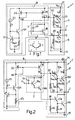
- Number 1 in Figure 1 indicates an operational amplifier comprising a differential input stage 2 shown only schematically and not described in detail; and a power stage 3 connected to the output 4 of differential input stage 2.
- Power stage 3 in turn comprises a gain stage 5; a power output stage 6 connected to gain stage 5 and defining an output terminal 7 supplying an output signal V o ; and a current source stage 8 for biasing output stage 6.
- Output stage 6 comprises two NPN transistors 12, 13 in Totem-Pole configuration; transistor 12 has the emitter terminal connected to output terminal 7, the base terminal defining a node 35, and the collector terminal connected to a supply line 14 (at supply voltage V cc ): transistor 13 has the emitter terminal connected to a ground line 15, the base terminal defining a node 36, and the collector terminal connected to output terminal 7; and transistors 12, 13 occupy respective areas A 12 , A 13 , have respective inverted saturation currents I s,12 , I s,13 and respective voltages V be,12 , V be,13 between the base and emitter terminals, and are supplied with respective currents I 12 , I 13 .
- Output stage 6 also comprises two resistors 16 and 17 of the same resistance R and located between the base and emitter terminals of respective transistors 12 and 13.
- Gain stage 5 comprises an NPN transistor 18 with the base terminal connected to output 4 of input stage 2, the collector terminal connected to the base terminal of transistor 12 (node 35), and the emitter terminal connected to the base terminal of transistor 13; and a stabilizing capacitor 19 located between the base and collector terminals of transistor 18.
- Current source stage 8 comprises an NPN reference transistor 21 with the emitter terminal connected to ground line 15, the collector terminal connected to supply line 14 via an equivalent current source 22, and the base terminal connected to ground line 15 via a resistor 23 of resistance R/2, where R is the resistance of resistors 16, 17 as indicated above.
- Reference transistor 21 has an area A 21 and a voltage drop V be,21 between the base and emitter terminals; and equivalent current source 22 supplies a current I r to reference transistor 21.
- a transistor 24 has the base and emitter terminals connected respectively to the collector and base terminals of reference transistor 21, and the collector terminal defining a node 38.
- current source stage 8 comprises two PNP transistors 25, 26 arranged so as to form a current mirror. More specifically, transistors 25, 26 have the base terminals connected to each other, and the emitter terminals connected to supply line 14; transistor 25 has the collector and base terminals connected to each other and to node 38; and transistor 26 has the collector terminal connected to node 35 of output stage 6 to which it supplies a bias current I p proportional to current I r supplied by equivalent current source 22.
- I r I s ,21 exp( V be ,21 V t )
- resistance R of resistor 16 must be fairly low to ensure the excess current, with respective to the quiescent condition, is sufficient to supply the increase in current at the base of transistor and the increase in current in resistor 16 due to the increase in voltage between the base and emitter of transistor 12.
- resistance R affects the quiescent current via the base current; and, by establishing the maximum permissible error via the ratio between the actual and nominal quiescent currents I 12,r /I' 12 , the minimum R value may be calculated as follows: R ⁇ ⁇ V t I ' 12 ⁇ ln I 12,r I ' 12
- the power stage in this case indicated 3', comprises a gain stage 5', which differs from gain stage 5 by presenting, as opposed to transistor 18, a first pair of transistors 18a, 18b in Darlington configuration.
- Power stage 3' also comprises an output stage 6', which differs from output stage 6 by presenting, instead of transistors 12 and 13, a second pair of transistors 12a, 12b and a third pair of transistors 13a, 13b also in Darlington configuration.
- Transistors 12a, 12b, 13a, 13b of output stage 6' respectively present base-emitter voltages V be,12a , V be,12b , V be,13a , V be,13b ; saturation currents I s,12a , I s,12b , I s,13a , I s,13b ; and areas A 12a , A 12b , A 13a , A 13b .
- Output stage 6' also differs from output stage 6 by presenting, instead of resistors 16 and 17, resistors 28, 29 located between the base and emitter terminals of respective transistors 12a, 13a, and resistors 30, 31 interposed between the base and emitter terminals of respective transistors 12b, 13b. Resistors 28, 29, 30 and 31 all have the same resistance value R 1 .
- Bias current I p1 supplied by current source stage 8, in which resistor 23 now has a resistance value of R/4, equals: I p 1 4 ⁇ V t R ⁇ ln I r I s ,21
- the quiescent current value may be regulated by working on the resistance value.
- the quiescent currents are controlled by simply providing additional resistive elements in the output stage, i.e. with no need for complex circuit networks, so that the circuit is simple in design, easy to integrate, reliable by virtue of its parameters being accurately controllable, and presents a small area.
- the power stage so formed comprises exclusively NPN power transistors, which are superior to PNP transistors as regards frequency response and size; presents no local feedback loops; can withstand capacitive loads of up to a few tens of nF with no need for a Boucherot cell; and presents a wide band.
- the topology of the power stage described is similar to that of Totem-Pole TTL devices, which, however, operate in class C with digital logic.
- the stage according to the invention provides for class AB biasing, and may be used in low-distortion analog applications.
Landscapes
- Engineering & Computer Science (AREA)
- Power Engineering (AREA)
- Amplifiers (AREA)
Priority Applications (4)
| Application Number | Priority Date | Filing Date | Title |
|---|---|---|---|
| EP96830235A EP0803975B1 (de) | 1996-04-26 | 1996-04-26 | Leistungsstufe für einen Operationsverstärker |
| DE69628911T DE69628911D1 (de) | 1996-04-26 | 1996-04-26 | Leistungsstufe für einen Operationsverstärker |
| US08/839,231 US5952881A (en) | 1996-04-26 | 1997-04-24 | Power stage, particularly for an operational amplifier |
| JP9108395A JPH1041759A (ja) | 1996-04-26 | 1997-04-25 | オペアンプ用電力段 |
Applications Claiming Priority (1)
| Application Number | Priority Date | Filing Date | Title |
|---|---|---|---|
| EP96830235A EP0803975B1 (de) | 1996-04-26 | 1996-04-26 | Leistungsstufe für einen Operationsverstärker |
Publications (2)
| Publication Number | Publication Date |
|---|---|
| EP0803975A1 true EP0803975A1 (de) | 1997-10-29 |
| EP0803975B1 EP0803975B1 (de) | 2003-07-02 |
Family
ID=8225886
Family Applications (1)
| Application Number | Title | Priority Date | Filing Date |
|---|---|---|---|
| EP96830235A Expired - Lifetime EP0803975B1 (de) | 1996-04-26 | 1996-04-26 | Leistungsstufe für einen Operationsverstärker |
Country Status (4)
| Country | Link |
|---|---|
| US (1) | US5952881A (de) |
| EP (1) | EP0803975B1 (de) |
| JP (1) | JPH1041759A (de) |
| DE (1) | DE69628911D1 (de) |
Families Citing this family (2)
| Publication number | Priority date | Publication date | Assignee | Title |
|---|---|---|---|---|
| US6292057B1 (en) * | 1998-12-18 | 2001-09-18 | Texas Instruments Incorporated | Output stage of an operational amplifier and method having a latchup-free sourcing current booster for driving low impedance loads |
| US6100763A (en) * | 1999-03-29 | 2000-08-08 | Motorola, Inc. | Circuit for RF buffer and method of operation |
Citations (3)
| Publication number | Priority date | Publication date | Assignee | Title |
|---|---|---|---|---|
| US3903479A (en) * | 1974-01-24 | 1975-09-02 | Rca Corp | Transistor base biasing using semiconductor junctions |
| US4295101A (en) * | 1979-12-10 | 1981-10-13 | Rca Corporation | Class AB push-pull quasi-linear amplifiers |
| DE3920802A1 (de) * | 1989-06-24 | 1991-01-10 | Telefunken Electronic Gmbh | Pull- und push-verstaerkerschaltung mit ruhestromstabilisierung |
Family Cites Families (2)
| Publication number | Priority date | Publication date | Assignee | Title |
|---|---|---|---|---|
| US4078207A (en) * | 1977-01-07 | 1978-03-07 | Rca Corporation | Push-pull transistor amplifier with driver circuitry providing over-current protection |
| US5019789A (en) * | 1990-06-26 | 1991-05-28 | Burr-Brown Corporation | Adaptive bias circuit for preventing turnoff in a push-pull stage |
-
1996
- 1996-04-26 EP EP96830235A patent/EP0803975B1/de not_active Expired - Lifetime
- 1996-04-26 DE DE69628911T patent/DE69628911D1/de not_active Expired - Lifetime
-
1997
- 1997-04-24 US US08/839,231 patent/US5952881A/en not_active Expired - Lifetime
- 1997-04-25 JP JP9108395A patent/JPH1041759A/ja active Pending
Patent Citations (3)
| Publication number | Priority date | Publication date | Assignee | Title |
|---|---|---|---|---|
| US3903479A (en) * | 1974-01-24 | 1975-09-02 | Rca Corp | Transistor base biasing using semiconductor junctions |
| US4295101A (en) * | 1979-12-10 | 1981-10-13 | Rca Corporation | Class AB push-pull quasi-linear amplifiers |
| DE3920802A1 (de) * | 1989-06-24 | 1991-01-10 | Telefunken Electronic Gmbh | Pull- und push-verstaerkerschaltung mit ruhestromstabilisierung |
Also Published As
| Publication number | Publication date |
|---|---|
| DE69628911D1 (de) | 2003-08-07 |
| EP0803975B1 (de) | 2003-07-02 |
| US5952881A (en) | 1999-09-14 |
| JPH1041759A (ja) | 1998-02-13 |
Similar Documents
| Publication | Publication Date | Title |
|---|---|---|
| GB2237947A (en) | Reducing parasitic capacitance induced distortion | |
| US4951003A (en) | Differential transconductance circuit | |
| EP0979552A1 (de) | Verstärker mit variabler verstärkung, hoher linearität und grosser bandbreite | |
| KR20010082344A (ko) | 레벨 시프트 회로 | |
| EP0209987A2 (de) | Pufferverstärker mit Verstärkungsfaktor Eins | |
| US5923216A (en) | Frequency selective amplifier circuit | |
| EP0502056B1 (de) | Differenzverstärker mit eingangsdämpfungsglied | |
| US5939944A (en) | NPN push-pull output stage with folded cascode JFETs | |
| US5115206A (en) | Merged differential amplifier and current source | |
| US4217555A (en) | Amplifier circuit arrangement with stabilized power-supply current | |
| US4360786A (en) | Variable-gain differential amplifier | |
| EP0803975B1 (de) | Leistungsstufe für einen Operationsverstärker | |
| EP0397265B1 (de) | Bipolare Transistorschaltung mit Verzerrungsausgleich | |
| US4612513A (en) | Differential amplifier | |
| US4521739A (en) | Low offset voltage transistor bridge transconductance amplifier | |
| EP0916182A1 (de) | Emitterschaltungsausgangsstufe mit hoher verstärkung | |
| US4593252A (en) | Enhanced transconductance amplifier | |
| GB2222043A (en) | Integrated wideband amplifier with current mirror feedback bias arrangement | |
| EP1225691B1 (de) | Schnelle Eingangsstufe für A-B Verstärker mit Basisstromkompensation für schnelles Einschwingen | |
| US6404285B1 (en) | Transistor amplifier that accommodates large input signals | |
| US6175226B1 (en) | Differential amplifier with common-mode regulating circuit | |
| JPH0697725B2 (ja) | 増幅器回路 | |
| US3421100A (en) | Direct coupled amplifier including twostage automatic gain control | |
| JPS61274518A (ja) | ディジタル―アナログ変換器のためのビット電流調整回路 | |
| US5313171A (en) | High speed, low distortion amplifier design and method |
Legal Events
| Date | Code | Title | Description |
|---|---|---|---|
| PUAI | Public reference made under article 153(3) epc to a published international application that has entered the european phase |
Free format text: ORIGINAL CODE: 0009012 |
|
| AK | Designated contracting states |
Kind code of ref document: A1 Designated state(s): DE FR GB IT |
|
| 17P | Request for examination filed |
Effective date: 19980218 |
|
| RAP3 | Party data changed (applicant data changed or rights of an application transferred) |
Owner name: STMICROELECTRONICS S.R.L. |
|
| 17Q | First examination report despatched |
Effective date: 20020108 |
|
| GRAG | Despatch of communication of intention to grant |
Free format text: ORIGINAL CODE: EPIDOS AGRA |
|
| GRAG | Despatch of communication of intention to grant |
Free format text: ORIGINAL CODE: EPIDOS AGRA |
|
| GRAH | Despatch of communication of intention to grant a patent |
Free format text: ORIGINAL CODE: EPIDOS IGRA |
|
| GRAH | Despatch of communication of intention to grant a patent |
Free format text: ORIGINAL CODE: EPIDOS IGRA |
|
| GRAA | (expected) grant |
Free format text: ORIGINAL CODE: 0009210 |
|
| AK | Designated contracting states |
Designated state(s): DE FR GB IT |
|
| PG25 | Lapsed in a contracting state [announced via postgrant information from national office to epo] |
Ref country code: FR Free format text: LAPSE BECAUSE OF FAILURE TO SUBMIT A TRANSLATION OF THE DESCRIPTION OR TO PAY THE FEE WITHIN THE PRESCRIBED TIME-LIMIT Effective date: 20030702 |
|
| REG | Reference to a national code |
Ref country code: GB Ref legal event code: FG4D |
|
| REF | Corresponds to: |
Ref document number: 69628911 Country of ref document: DE Date of ref document: 20030807 Kind code of ref document: P |
|
| PG25 | Lapsed in a contracting state [announced via postgrant information from national office to epo] |
Ref country code: DE Free format text: LAPSE BECAUSE OF FAILURE TO SUBMIT A TRANSLATION OF THE DESCRIPTION OR TO PAY THE FEE WITHIN THE PRESCRIBED TIME-LIMIT Effective date: 20031003 |
|
| PLBE | No opposition filed within time limit |
Free format text: ORIGINAL CODE: 0009261 |
|
| STAA | Information on the status of an ep patent application or granted ep patent |
Free format text: STATUS: NO OPPOSITION FILED WITHIN TIME LIMIT |
|
| 26N | No opposition filed |
Effective date: 20040405 |
|
| EN | Fr: translation not filed | ||
| PG25 | Lapsed in a contracting state [announced via postgrant information from national office to epo] |
Ref country code: IT Free format text: LAPSE BECAUSE OF NON-PAYMENT OF DUE FEES;WARNING: LAPSES OF ITALIAN PATENTS WITH EFFECTIVE DATE BEFORE 2007 MAY HAVE OCCURRED AT ANY TIME BEFORE 2007. THE CORRECT EFFECTIVE DATE MAY BE DIFFERENT FROM THE ONE RECORDED. Effective date: 20050426 |
|
| PGFP | Annual fee paid to national office [announced via postgrant information from national office to epo] |
Ref country code: GB Payment date: 20070328 Year of fee payment: 12 |
|
| GBPC | Gb: european patent ceased through non-payment of renewal fee |
Effective date: 20080426 |
|
| PG25 | Lapsed in a contracting state [announced via postgrant information from national office to epo] |
Ref country code: GB Free format text: LAPSE BECAUSE OF NON-PAYMENT OF DUE FEES Effective date: 20080426 |